行政院國家科學委員會專題研究計畫 成果報告
高度微縮金氧半場效電晶體機械應力效應之研究(3/3)
計畫類別: 個別型計畫
計畫編號: NSC94-2215-E-009-005-
執行期間: 94 年 08 月 01 日至 95 年 07 月 31 日
執行單位: 國立交通大學電子工程學系及電子研究所
計畫主持人: 陳明哲
計畫參與人員: 許義明,謝振宇,李建志,李韋漢,林以唐,梁惕華,呂立方,
周佳宏,簡鶴年,陳彥銘,宋東壕
報告類型: 完整報告
處理方式: 本計畫可公開查詢
中 華 民 國 95 年 10 月 30 日
1
行政院國家科學委員會補助專題研究計畫成果報告
※※※※※※※※※※※※※※※※※※※※※※
※
高度微縮金氧半場效電晶體機械應力效應之研究(3/3)
※
※※※※※※※※※※※※※※※※※※※※※※※
計畫類別:▓個別型計畫 □整合型計畫
計畫編號:
NSC 94-2215-E-009-005-
執行期間:
94/08/01 ~ 95/07/31
計畫主持人:陳明哲
計畫參與人員:
許義明
,
謝振宇
,
李建志
,
李韋漢
,林以唐,
梁惕華,呂立方,周佳宏,簡鶴年,陳彥銘,宋東壕
成果報告類型(依經費核定清單規定繳交):□精簡報告 ▓完整報告
本成果報告包括以下應繳交之附件:
□赴國外出差或研習心得報告一份
□赴大陸地區出差或研習心得報告一份
□出席國際學術會議心得報告及發表之論文各一份
□
國際合作研究計畫國外研究報告書一份
處理方式:除產學合作研究計畫、提升產業技術及人才培育研究計畫、列管計畫
及下列情形者外,得立即公開查詢
□涉及專利或其他智慧財產權,□一年□二年後可公開查詢
執行單位:國立交通大學電子工程學系
中 華 民 國 95 年 10 月 28 日
2
行政院國家科學委員會補助專題研究計畫成果報告
高度微縮金氧半場效電晶體機械應力效應之研究(3/3)
The Impact of Mechanical Stress in Highly Scaled MOSFETs (3/3)
執行期限: 94/08/01 ~ 95/07/31
計畫編號: NSC 94-2215-E-009-005-
主持人:陳明哲教授 國立交通大學電子工程學系
一、中文摘要
本計畫探索下世代場效電晶體機械應力效應 之嶄新領域,將配合當年度互補式金氧半場效電 晶體製程技術演進同時執行八大項目: 1. 以當年度最先進製程製作 n- and p-型 高度微 縮金氧半場效電晶體元件,以金氧半場效電晶體 微縮尺寸和閘極至淺槽隔離邊緣距離二者為圖案 變動參數。 進行電流電壓/電容電壓量測。以自 行發展的一維量子力學模擬器與實驗比較以萃取 重要製程參數。 2. 執行二維製程及機械應力之模擬以萃取張力 之分佈, 大小並決定其性質。 3. 定義不同機械應力條件即將萃取得到的張力 大小表達為不同製程參數, 不同場效電晶體微縮 尺寸, 和不同閘極至淺槽隔離邊緣距離的函數。 4. 以自行發展的量子力學模擬器計算不同機械 應力條件下反置通道二維電子(洞)氣及次能帶分 佈,以獲得遷移率等重要參數。建立機械應力之 理論架構並導出張力解析模式。 5. 低溫實驗萃取通道彈道傳輸係數以與機械應 力作一關聯。 6. 二維量子力學彈道傳輸模擬器之程式撰寫,除 錯及執行。 7. 低頻雜訊及電報雜訊量測以偵測機械應力之 細微變化。 8. 機械應力效應置入電路模擬器場效電晶體模 式並進行電路功能方塊模擬。 本計畫目的即為藉著上述執行項目以肇清機 械應力對下世代場效電晶體元件性能之效應及介 觀物理機制,另方面將機械應力效應置入電路模擬 器場效電晶體模式以進行正確的積體電路設計, 進而使得系統單晶片積體電路設計複雜化及高密 度化能有效解除機械應力之威脅。 關鍵詞:場效電晶體; 機械應力; 張力; 二維電子 氣; 二維電洞氣; 通道彈道傳輸; 低頻雜訊; 電 報雜訊; 模式; 積體電路設計。英文摘要
The project explores the mechanical stress issue on the highly scaled MOSFETs. Following are the eight main items to be conducted along with state-of-the-art CMOS scaled technologies: 1. Fabricate n- and p-type highly scaled MOSFETs
by advanced process technologies, followed by I-V/C-V characterization as well as our developed 1-D quantum mechanical I-V/C-V simulation to extract key process parameters.
2. Perform a two-dimensional process/mechanical stress simulator to extract the magnitude and distribution of strain and determine its property.
3. Experimentally define mechanical stress conditions in terms of strain expressed as function of process parameters, FET scaling factor, and distance between gate to STI (shallow trench isolation) edge.
4. Perform our developed 1-D quantum mechanical simulators to assess 2-dimensional electron (hole) gas and sub-band distributions, leading to extraction of relevant parameters like mobility. Establish theoretical framework of mechanical stress and develop analytic model of strain. 5. Perform low-temperature experiment to extract
channel backscattering coefficients and relate them to mechanical stress.
6. Establish 2-D quantum mechanical ballistic simulators.
7. Perform low frequency noise and random telegraph signal experiment to detect some change in mechanical stress.
8. Incorporate mechanical stress into SPICE MOSFET model and perform simulation on functional circuit blocks.
The goal of the project is to clarify the impact of mechanical stress on next generation MOSFETs and the underlying mesoscopic physical mechanisms. Meanwhile, incorporation of mechanical stress into SPICE MOSFET model enables correct IC design and as a result, we can reach a a complex, highly dense SOC design effectively free of the harmful mechanical stress.
3 Key Words:MOSFET; Mechanical Stress; Strain;
2-Dimensional Electron Gas; 2-Dimensional
Hole Gas; Channel Ballistic Transport;
Low-Frequency Noise; Random Telegraph Signal;
Model; IC Design
二、緣由與目的
依 照 International Technology Roadmap for Semiconductors,在下世代 Silicon CMOS 製程技術演進 過程當中, MOSFET 尺寸持續微縮且 Gate 極亦持續更為 靠近 STI(Shallow Trench Isolation)邊緣,衍生的機械 應力(Mechanical Stress)已有文獻報告對元件推動電流 產生衰減或其他影響,此問題對於積體電路設計複雜化 及高密度化之趨勢(尤其是系統單晶片設計 SOC)不利,故 以機械應力效應為議題的研究最近在國際上受到高度重 視。 我們過去數年經驗的累積反映出一個有系統的嚴 謹性的機械應力效應研究是十分緊迫的,此為本計畫提 出之背景: 1 在我們最近發表的創見性的一超大型級之測試載具晶 片, 內含有一連串高敏感度之測試結構, 用以偵測超大 型晶片在不同製程技術製造下之可靠度分析, 並提出一 新的應力模組理論, 來估算晶片故障分布與故障機構模 式。結果呈現超大型晶片故障之韋博統計分布與晶片幾 何大小, 封裝材料相關。此外由應力分析模擬和針壓實 驗, 我們找到一最佳抗應力緩衝層鍍於輸出入墊片上 方。再將靜電放電保護元件及環狀振盪電路置於輸出入 墊片下方。在傳輸線脈衝高壓測試下,輸出入墊片下之靜 電放電保護元件的二次崩潰電壓和電流曲線仍具優秀的 特性。而在直流與交流實驗測試下, 輸出入墊片下之環 狀振盪電路的傳播延遲時間仍然保留在大約 20 微微秒 左右。 2. 本研究群這幾年已自行發展出 1-D 量子力學(Quantum Mechanical) I-V/C-V numerical 模擬器, 能計算出 Inversion Channel 因 Quantum Confinement 效應引致 的 二 維 電 子 氣 (2DEG) 或 二 維 電 洞 氣 (2DHG) 及 其 Sub-bands 分佈大小等。本計畫將此基礎延伸至 2-D Quantum Mechanical Ballistic 模擬器程式撰寫,除錯及 執行以反映最近趨勢。
3.萃取 Channel Backscattering Coefficients 的低溫 實驗方法已在 2002 IEDM 發表。
4.本研究群亦已成功建立高度靈敏低頻雜訊量測系統及 時域擾動量測系統。
本計畫目的即肇清機械應力對下世代 FET 元件性 能之效應及介觀物理機制,另方面將機械應力效應置入 SPICE MOSFET Model 以進行正確的 IC Design,進而使 得 SOC 積體電路設計複雜化及高密度化之同時,能有效 解除機械應力之威脅。
三、研究方法與成果
1.我們在 Highly Scaled MOSFETs (即以 MOSFET 微縮尺 寸和 Gate 極至 STI 邊緣距離二者為 Layout 變動參數) 上量測不同機械應力條件下之 I-V 特性,實驗發現機 械應力確會降低 n-Channel MOSFETs 元件推動電流但 增加 p-Channel MOSFETs 元件推動電流,與文獻上發 表者 不同。
2.完成量子力學 I-V/C-V 模擬與實驗比較並萃取重要參
數 如 poly doping, substrate doping, flatband voltage, 有效氧化層厚度。
3.完成二維製程及機械應力之模擬並萃取決定 Strain 之 分佈, 大小, 性質。
4.完成萃取得到的 Strain 大小表達為不同製程參數, 不 同 MOSFET 微縮尺寸, 和不同 Gate 極至 STI 邊緣距離的 函數。
5.Currently we are calculating 量子力學模擬計算不 同機械應力條件下 Inversion Channel 二維電子(洞)氣 及 Sub-bands 分佈,並獲得 Mobility 等重要參數。 6. Currently we are improving Mechanical Stress 之理論架構建立並導出 Strain 解析模式。
7.
Currently we are conducting scattering 實驗 萃取 Channel Backscattering Coefficients 並與 strain 應力作一 Correlation。四、 結論與討論
(1) 低頻雜訊拿來使用在監控受不同的製程應力程度下 的氧化層介面品質, 在承受製程應力的金氧半電晶體中的 低頻雜訊量測中,發現靠近表面的缺陷密度隨著通道寬度 而變化。 這個發現可以解釋為在矽和氧化矽的介面間, 因 為晶格長度不匹配所造成的 Pb 中心可視為靠近表面的缺 陷的主要來源。在低頻雜訊的實驗中,對於通道寬度的縮 減,相對應於應力的提高,也降低晶格長度不匹配的程度。 (2) 在產製下世代受應力電子元件 Strain Engineering 領域最近作出了重大貢獻---- 針對 Uniaxial Strain 下 Impurities (特別是 Boron, 為目前高度挑戰卻也爭議性 極大的題目) 在 Silicon 的高溫特殊擴散行為提出前所 未有、嶄新物理模式並獲得實驗支持:M. J. Chen and Y. M. Sheu, “Effect of uniaxial strain on anisotropic diffusion in silicon,” Applied Physics Letters, vol. 89, pp. 161908-1-181908-3, Oct. 2006.
以下為APL國際評審給的 Evaluation Summary:
Paper Interesting: Yes Original Paper: Yes Sufficient Physics: Yes Well Organized and Clear: Yes Free From Errors: Yes Conclusions Supported: Yes Appropriate Title: Yes Good Abstract: Yes Satisfactory English: Yes Adequate References: Yes Clear Figures: Yes
OVERALL RATING: Excellent
(3) 本人已將奈米線研究(一篇有關研究電流流經奈米線狀
的 percolation path 的 APL 論文被德國以及希臘的頂尖大 學研究團隊所引用於發表在 2005 APL 和 2006 PRB 的論 文 之 中) 延 伸 至 奈 米 碳 管 電 晶 體 , 發 表 了 一 篇 Applied Physics Letters論文 (此為跨領域論文,本人為通訊作者) :
M. P. Lu, C. Y. Hsiao, P. Y. Lo, J. H. Wei, Y. S. Yang, and M. J. Chen, “Semiconducting single-walled carbon nanotubes exposed to distilled water and aqueous solution: electrical measurement and theoretical
4 calculation,” Applied Physics Letters, vol. 88, pp. 053114-1—053114-3, Feb. 2006.
此論文探討生物樣本電性量測及應用量子力學理論計
算, 特別為 APL 國際評審高度認定。亦被選入兩本知名的
學術網路期刊:
z Selected Articles in Virtual Journal of Nanoscale
Science & Technology, Vol. 13, Issue 6, 2006.
z Selected Articles in Virtual Journal of Biological
Physics Research, Vol. 11, Issue 4, 2006.
(4) 庫倫能量(Coulomb energy)是針對電子填滿在氧化層 之內的奈米尺寸陷阱(Nanometer-Scale Trap),傳統的庫倫 能量只考慮在表面的陷阱,在我們的研究之中,我們針對 1.7 奈米厚度的氧化層元件所做的實驗驗證:比較深入的缺 陷 會 造 成 庫 倫 能 量 的 增 高 , 另 外 一 個 證 據 來 自 於 multiphonon 理論,可以解釋電子被缺陷抓住和釋放的能量 交換,我們更進ㄧ步闡述我們所描寫的庫倫能量和ㄧ般在 記憶體元件中電子填充量子點(Quantum Dot)或量子晶體 (Nanocrystal)記憶體所面對的庫倫能量在物理上(即能量系 統圖)是相當有所關連的:
z M. P. Lu and M. J. Chen, “Oxide-trap-enhanced Coulomb energy in a metal-oxide-semiconductor system”, Physical Review B, vol. 72, pp. 235417-1—235417-5, December 2005.
簡言之,此篇論文為相關領域二十幾年以來所作最好的, 且為兩位國際評審認定,並被 American Journal Experts 所注意到,這是一個來自全美 Top 10 大學的研究生所成立 的組織,其中有研究相關奈米領域的研究生,他在信中提 及“was impressed by the quality of the research and the
thought behind your article”。以嚴謹的物理探討延伸至量 子點(Quantum Dot)或量子晶體(Nanocrystal), 將能提出 新的設計方法以因應奈米尺度的微觀世界。
參考文獻(發表論文):
1. Y. M. Sheu, C. S. Chang, H. C. Lin, S. S. Lin, C. H. Lee, C. C. Wu, M. J. Chen, C. H. Diaz, “Impact of STI Mechanical Stress in Highly Scaled MOSFETs,” IEEE Symposium on VLSI-TSA, Technical Digest, pp. 269-272, 2003.
2. Y. M. Sheu, Kelvin Y. Y. Doong, C. H. Lee, M. J. Chen, C. H. Diaz, “Study on STI Mechanical Stress Induced Variation in 90-nm CMOSFETs,” IEEE International Conference on Microelectronic Test Structures, pp. 205-208, 2003.
3. M. J. Chen, H. T. Huang, Y. C. Chou, R. T. Chen, Y. T. Tseng, P. N. Chen, and C. H. Diaz, “Separation of Channel Backscattering Coefficients in Nanoscale MOSFETs,” IEEE Trans. Electron Devices, vol. 51, pp.1409-1415, September 2004.
4. Y. M. Sheu, S. J. Yang, C. C. Wang, C. S. Chang, L. P. Huang, T. Y. Huang, M. J. Chen, C. H. Diaz, “Modeling mechanical stress effect on dopant diffusion in scaled MOSFETs,” IEEE Trans. Electron Devices, vol.52, pp. 30-38, January 2005.
5. M. J. Chen, R. T. Chen, and Y. S. Lin, “Decoupling channel backscattering coefficients in nanoscale MOSFETs to establish near-source channel conduction-band profiles,” Silicon Nanoelectronics Workshop, pp. 50-51, June 2005. (Kyoto). 6. M. P. Lu and M. J. Chen, “Oxide-trap-enhanced Coulomb energy
in a metal-oxide-semiconductor system”, Physical Review B, vol. 72, pp. 235417-1—235417-5, December 2005.
7. M. P. Lu, C. Y. Hsiao, P. Y. Lo, J. H. Wei, Y. S. Yang, and M. J. Chen, “Semiconducting single-walled carbon nanotubes exposed to distilled water and aqueous solution: electrical measurement
and theoretical calculation,” Applied Physics Letters, vol. 88, pp. 053114-1—053114-3, Feb. 2006. Selected Articles in Virtual Journal of Nanoscale Science & Technology, Vol. 13, Issue 6, 2006; and Selected Articles in Virtual Journal of Biological Physics Research, Vol. 11, Issue 4, 2006.
8. M. P. Lu, W. C. Lee, M. J. Chen, “Channel-width dependence of low-frequency noise in process tensile-strained n-channel metal-oxide-semiconductor transistors,” Applied Physics Letters, vol. 88, pp. 063511-1—063511-3, Feb. 2006.
9. C. Y. S. Cho, M. J. Chen, C. F. Chen, P. Tuntasood, D. T. Fan, and T. Y. Liu, “A novel self-aligned highly reliable sidewall split-gate Flash memory,” IEEE Trans. Electron Devices, vol. 53, pp. 465-473, March 2006.
10. Y. M. Sheu, S. J. Yang, C. C. Wang, C. S. Chang, M. J. Chen, S. Liu, and C. H. Diaz, “Reproducing subthreshold characteristics of metal-oxide-semiconductor field effect transistors under shallow trench isolation mechanical stress using a stress-dependence diffusion model,” Japanese Journal of Applied Physics, vol. 45, pp. L849-L851, August 2006.
11. Y. M. Sheu, K. W. Su, S. Tian, S. J. Yang, C. C. Wang, M. J. Chen, and S. Liu, “Modeling the well-edge proximity effect in highly-scaled MOSFETs,” IEEE Trans. Electron Devices, vol. 53, pp. 2792-2798, Nov. 2006.
12. M. J. Chen and Y. M. Sheu, “Effect of uniaxial strain on anisotropic diffusion in silicon,” Applied Physics Letters, vol. 89, pp. 161908-1-181908-3, Oct. 2006.
Important Figures and Tables
0.1 1 10 1017 1018 1019 T rap D ensity (cm -3 eV -1 ) Channel Width (μm) 0.0 0.2 0.4 0.6 0.8 1.0 0.0 0.1 0.2 0.3 0.4 Vgo= 0.25 V Vgo= 0.75 V Vgo= 0.5 V Dr ai n Cu rr e n t De n si ty
(
mA / μ m)
V
D(V)
W = 10 μm W= 0.11 μm5 ( a )
SiO
2 Si C E C E Trap A Trap B V E V E nm 7 . 0 ( b ) ω h S state free state bound T E E0− B E state free state bound ω h S T E E0− B E Configuration Coordinate → B Trap Trap A 3.2 eV 3.3 eV E lect ro n ic + E la st ic E n e rg y ↓ ( a )SiO
2 Si C E C E Trap A Trap B V E V E nm 7 . 0 ( b ) ω h S state free state bound T E E0− B E state free state bound ω h S T E E0− B E Configuration Coordinate → B Trap Trap A 3.2 eV 3.3 eV E lect ro n ic + E la st ic E n e rg y ↓Ground
depC
invC
GV
q
−
GQ
depQ
invQ
gC
cC
Ground
depC
invC
GV
q
−
GQ
depQ
invQ
gC
cC
0.2
0.3
0.4
10
-110
010
110
2τ
c/
τ
eV
G(V)
Exp. Trap A Exp. Trap B Eox-ET= 3.3 eV, zT= 0 nm Eox-ET= 3.2 eV, zT= 0.7 nm T ox E E− E0 ox T substrate Si Oxide T Z F E T ox E E− E0 ox T substrate Si Oxide T Z F E0.2
0.3
0.4
10
-110
010
110
2τ
c/
τ
eV
G(V)
Exp. Trap A Exp. Trap B Eox-ET= 3.3 eV, zT= 0 nm Eox-ET= 3.2 eV, zT= 0.7 nm T ox E E− E0 ox T substrate Si Oxide T Z F E T ox E E− E0 ox T substrate Si Oxide T Z F E 100 101 102 103 104 105 10-14 10-12 10-10 10-8 S Vg (V 2 /H z) Frequency (Hz) W= 0.11 μm, L=0.5 μm Vgo= 0.6 V, VD= 0.2 V Device A Device B Device C f -10.1
1
10
10
-1310
-1210
-1110
-10S
Vg(V
2/H
z
)
Channel Width (
μm)
L= 0.5 μm, V D= 0.2 V V go= 0.6 V, f= 100 Hz0.1
1
10
0
10
20
30
I
DsatG
a
in (%)
Channel Width (
μ
m)
L= 0.5
μ
m
V
go=0.75 V
V
D=1 V
6
7
Effect of uniaxial strain on anisotropic diffusion in silicon
Ming-Jer Chena兲 and Yi-Ming SheuDepartment of Electronics Engineering, National Chiao Tung University, Hsin-Chu 300, Taiwan
共Received 9 June 2006; accepted 30 August 2006; published online 17 October 2006兲
A physical model is directly extended from the thermodynamic framework to deal with anisotropic diffusion in uniaxially stressed silicon. With the anisotropy of the uniaxial strain induced activation energy as input, two fundamental material parameters, the activation volume and the migration strain anisotropy, can be quantitatively determined. When applied to boron, a process-device coupled simulation is performed on a p-type metal-oxide-semiconductor field-effect transistor undergoing uniaxial stress in a manufacturing process. The resulting material parameters have been found to be in satisfactory agreement with values presented in the literature. © 2006 American
Institute of Physics. 关DOI:10.1063/1.2362980兴
Strain engineering has been widely recognized as an in-dispensable performance booster in producing next-generation metal-oxide-semiconductor field-effect transistors 共MOSFETs兲.1,2
There have been two fundamentally different methods used to achieve this goal:1,2 共i兲 biaxially strained silicon on a relaxed SiGe buffer layer and 共ii兲 uniaxially strained silicon through the use of trench isolation, silicide, and cap layers during the manufacturing process. However, diffusion in strained silicon is essentially different from that of unstrained silicon. Thus, an understanding of strain depen-dent diffusion, as well as its control, is a challenging issue. So far, there have been significant studies in this direction covering a wide range of experimental findings and confirmations,3–9 atomistic calculations,10–13 physical models,10–16 and technology computer-aided design.17 Spe-cifically, Cowern et al.5experimentally revealed a linear de-pendence of the activation energy on strain. Within the ther-modynamic framework constructed by Aziz et al.共see Ref.
18, which is more recent and more thorough than the earlier works cited above兲, the activation volume 共V˜兲 and the aniso-tropy of the migration volume共V˜储
m
− V˜⬜m兲 exist in nature. The combination of the activation energy, the activation volume, and the anisotropy of the migration volume is remarkable, as demonstrated in a physical model14–16,18 dedicated to both the hydrostatic pressure experiment and the in-plane biaxial stress experiment, V ˜ +3 2 Q33−biax
⬘
Ybiax = ±⍀ + 共V˜储 m − V˜⬜m兲, 共1兲 V ˜ +3 2 Q11−biax⬘
Ybiax = ±⍀ −1 2共V˜储 m − V˜⬜m兲, 共2兲where Q33−biax
⬘
is the biaxial strain induced activation energy in the direction normal to the silicon surface, Ybiax is thebiaxial modulus,⍀ is the lattice site volume, and Q11−biax
⬘
is the biaxial strain induced activation energy in the direction parallel to the surface.On the other hand, in the case of uniaxial stress as en-countered while fabricating the MOSFET, without the use of a relaxed SiGe buffer layer, the stress is created through the trench isolation, silicide, or cap layers in a manufacturing
process. Therefore, a straightforward extension to the uniaxial strain counterpart is essential. In this letter, one such model is derived and its linkage to the case of biaxial strain, Eqs. 共1兲 and 共2兲, is established. When applied to boron, a process-device coupled simulation is performed on a p-type MOSFET undergoing uniaxial stressing during the manufac-turing process, followed by a systematic assessment of the fundamental material parameters.
According to Aziz14 and Aziz et al.,18 in the case of equilibrium or a quickly equilibrated point defect, the effect of stress on the dopant diffusivity in the direction normal to a共001兲 surface can be written as
D33共兲 D33共0兲 = exp
冉
关V f+ V˜ 33 m兴 kBT冊
. 共3兲Here the product of the stress tensor and the formation strain tensor Vf is the work done against the stress field in defect formation, the product of the stress tensor and the migration strain tensor V˜33m is the work required for the tran-sition in the migration path, kB is Boltzmann’s constant, and
T is the diffusion temperature. The tensor Vf involves the
creation or annihilation of a lattice site, followed by a relax-ation process,14,18 Vf= ±⍀
冤
0 0 1冥
+V r 3冤
1 1 1冥
. 共4兲The⫹ sign denotes vacancy formation and the ⫺ sign rep-resents interstitial formation. The relaxation volume propa-gates elastically to all surfaces, resulting in a change in the volume of the crystal by an amount Vr. V˜
33 m
is expected to have the form14,18
V ˜ 33 m =
冤
V ˜ ⬜ m V ˜ ⬜ m V ˜ 储 m冥
. 共5兲 In Eq. 共5兲, V˜⬜m and V˜储 m, respectively, reflect the dimension changes perpendicular and parallel to the direction of the net transport when the point defect reaches its saddle point.14,18 Aziz further defined the activation volume as the sum of the
a兲Electronic mail: chenmj@faculty.nctu.edu.tw
APPLIED PHYSICS LETTERS 89, 161908共2006兲
0003-6951/2006/89共16兲/161908/3/$23.00 89, 161908-1 © 2006 American Institute of Physics
three diagonal elements of the formation strain tensor and the migration strain tensor, as expressed by
V
˜ = ± ⍀ + Vr
+ 2V˜⬜m+ V˜储
m
. 共6兲
It is well recognized12 that when applying a uniaxial stress in a certain direction parallel to the silicon surface, the solid will modify its shape in order to minimize the energy of the system. In other words, the solid will deform in such a way that each surface perpendicular to the applied stress di-rection becomes stress-free. The underlying stress tensor therefore is =uniax
冤
1 0 0冥
. 共7兲On the basis of Hooke’s law,uniax in the linear elastic
re-gime can be related to the uniaxial strainuniaxinduced in the same direction:uniax= Yuniaxuniax, where the uniaxial modu-lus Yuniax=共C11− 2C12兲 with Poisson’s ratio = C12/共C11
+ C12兲. C11and C12are the elasticity constants. Analogous to
previous work,5the uniaxial strain induced activation energy in the direction normal to the共001兲 surface, Q33−uniax
⬘
, can be linked to the underlying diffusivity,D33共uniax兲
D33共0兲
= exp
冉
−Q33−uniax⬘
uniaxkBT
冊
. 共8兲
By combining Eqs.共4兲,共5兲, and共7兲and equalizing Eqs.
共3兲–共8兲, one obtains Q33−uniax
⬘
/ Yuniax =−Vr/ 3 − V˜⬜m. Again, byincorporating Eq.共6兲, the following expression is produced: V
˜ + 3Q33−uniax
⬘
Yuniax
= ±⍀ + 共V˜m储 − V˜⬜m兲. 共9兲
It is then a straightforward task to derive the uniaxial strain induced activation energy Q11−uniax
⬘
in the applied stress di-rection: Q11−uniax⬘
/ Yuniax= −Vr/ 3 − V˜储 m . Consequently, a similar model is achieved, V ˜ + 3Q11−uniax
⬘
Yuniax = ±⍀ − 2共V˜储 m − V˜⬜m兲. 共10兲Obviously, the uniaxial strain version is closely related to its biaxial counterpart: by comparing Eqs. 共1兲 and 共9兲, Q33−uniax
⬘
=共Yuniax/ 2Ybiax兲Q33−biax⬘
is obtained. Anotherrelation can then be readily derived: Q11−uniax
⬘
= −共Yuniax/ 2Ybiax兲Q33−biax⬘
+共Yuniax/ Ybiax兲Q11−biax⬘
.To produce the experimental parameters in terms of the anisotropy of the uniaxial strain induced activation energy, a uniaxial stress experiment was carried out in terms of a p-channel MOSFET in a state-of-the-art manufacturing process.17 The channel length was maintained at 65 nm while changing the spacing in the channel length direction between the two trench isolation sidewalls. The topside lay-out is detailed elsewhere.17Under such a situation, the chan-nel zone encounters a compressive stress from the nearby trench isolation regions in the channel length direction. The devices used are quite wide共10m兲, meaning that the strain in the channel width direction is relatively negligible. The 共001兲 silicon surface is supposed to be stress free. This hy-pothesis has been validated using the sophisticated simula-tions detailed in Ref.17, which revealed that in the proxim-ity of the silicon surface, the stress in the channel length
direction is much larger in magnitude than that in the direc-tion normal to the surface. Therefore, the proposed physical model can be adequately applied. The effect of changing the spacing between the two trench isolation regions in the chan-nel length direction is reflected in the measured saturation threshold voltage, as displayed in Fig.1. The negative shift in the saturation threshold voltage with increasing stress共via decreasing spacing between the trench isolation regions兲 shown in Fig.1 can be attributed to the retarded boron dif-fusion.
A two-dimensional process-device coupled simulation, as detailed in Ref. 17, was slightly modified by taking the anisotropy of the boron diffusivity into account,
D33共t兲 D33共0兲 = exp
冉
− Q33−TCAD⬘
t kBT冊
, 共11兲 D11共t兲 D11共0兲 = exp冉
− Q11−TCAD⬘
t kBT冊
. 共12兲According to the work in Ref.17the total straintis the sum
of the three strain components: xx in the channel length
direction,yy in the channel width direction, and zz in the
direction normal to the silicon surface. From the simulated strain distributions, t⬃xx, leading to Q33−TCAD
⬘
⬇Q33−uniax⬘
and Q11−TCAD
⬘
⬇Q11−uniax⬘
. The simulated saturation threshold voltages for different values of Q33−uniax⬘
and Q11−uniax⬘
are plotted in Fig.1 for comparison. The figure clearly exhibits that 共i兲 the largest deviation occurs at Q33−uniax⬘
= 0 and Q11−uniax⬘
= 0, the case of no stress dependencies;共ii兲 the most accurate reproduction is achieved with the anisotropic acti-vation energies, rather than the isotropic variety; and共iii兲 the anisotropy of the activation energy must be adequate, that is, Q11−uniax⬘
= −7 eV per unit strain and Q33−uniax⬘
= −3.5 eV per unit strain are more favorable than Q11−uniax⬘
= −3.5 eV per unit strain and Q33−uniax⬘
= −7 eV per unit strain.FIG. 1. Measured p-MOSFET saturation threshold voltage vs the spacing between the nearby trench isolation sidewalls in the channel length direc-tion. Also shown are those共lines兲 from the process-device coupled simula-tion with and without the strain induced activasimula-tion energies. The reason that the “no stress-dependent diffusion curve” is not entirely horizontal is due to dopant segregation near the edges of the source/drain regions. Specifically, the nonuniformity is caused by boron segregation occurring close to trench isolation oxide during the thermal process. Although the affected profile is not in vicinity of the MOSFET core region, a minor threshold voltage dif-ference共⬃3 mV兲 between large and small active areas can still be observed, even without the stress-dependent diffusion model.
161908-2 M.-J. Chen and Y.-M. Sheu Appl. Phys. Lett. 89, 161908共2006兲
Prior to determining the fundamental material param-eters, a systematic treatment, such as that indicated in Fig.2, is demanded. In Fig.2a series of straight lines of Q11−uniax
⬘
vsQ33−uniax
⬘
are from Eqs. 共9兲 and 共10兲 for a literaturerange15,16,18 of V˜ and the migration strain anisotropy A˜ 共⬅共V˜储
m
− V˜⬜m兲/⍀兲.18 In the calculation procedure, the follow-ing literature values were employed:19共i兲 C11= 168 GPa and
C12= 65 GPa, giving rise to Yuniax= 131 GPa and= 0.28;共ii兲 ⍀=2.26⫻10−23cm3. The above experimental parameters
are also added to the figure. From the figure a set of V˜ and A˜ can be clearly located around the data point. On the other hand, uncertainties exist based on a series of literature data: V
˜ =−0.16±0.05 ⍀.18
Taking such uncertainties into account, Fig.2reveals that the data point does match the upper limit, that is, V˜ =−0.21 ⍀. The corresponding V˜储m− V˜⬜min the
vicin-ity of 0.15⍀ is determined accordingly, falling within the reasonable range.15,16,18 Such corroborating experimental evidence further indicates that the transient enhanced diffu-sion effect is relatively insignificant when compared to the long-term diffusion times in the underlying manufacturing process. Under such circumstances, the point defect is rap-idly equilibrated relative to the entire diffusion time.
Finally, we quoted the existing ab initio calculations:12,13 Q11−biax
⬘
= −19.2 eV per unit strain and Q33−biax⬘
= −13.9 eV per unit strain, which were transformed via the aforementioned relationship into the equivalent Q11−uniax⬘
of −8.77 eV per unit strain and Q33−uniax⬘
of −4.975 eV per unit strain. In thispro-cess, the Ybiax used was equal to 183 GPa according to
Ybiax=共C11+ C12−C12兲 with its Poisson’s ratio= 2C12/ C11.
Evidently, the two data points are quite comparable to each other, as displayed in Fig.2.
A physical model dealing with anisotropic diffusion in uniaxially stressed silicon is derived and is quantitatively connected to the biaxial case. A process-device coupled simulation is performed on a p-type MOSFET undergoing uniaxial stress during the manufacturing process. A system-atic treatment is conducted and the resulting fundamental material parameters are in satisfactory agreement with litera-ture values.
This research is supported by the National Science Council of Taiwan under Contract No. NSC94-2215-E-009-005.
1S. E. Thompson, M. Armstrong, C. Auth, M. Alavi, M. Buehler, R. Chau,
S. Cea, T. Ghani, G. Glass, T. Hoffman, C. H. Jan, C. Kenyon, J. Klaus, K. Kuhn, Z. Ma, B. Mcintyre, K. Mistry, A. Murthy, B. Obradovic, R. Nagi-setty, P. Nguyen, S. Sivakumar, R. Shaheed, L. Shifren, B. Tufts, S. Tyagi, M. Bohr, and Y. El-Mansy, IEEE Trans. Electron Devices 51, 1790 共2004兲.
2C. H. Ge, C. C. Lin, C. H. Ko, C. C. Huang, Y. C. Huang, B. W. Chen, B.
C. Perng, C. C. Sheu, P. Y. Tsai, L. G. Yao, C. L. Wu, T. L. Lee, C. J. Chen, C. T. Wang, S. C. Lin, Y. C. Yeo, and C. Hu, Tech. Dig. - Int. Electron Devices Meet. 2003, 73.
3N. Moriya, L. C. Feldman, H. S. Luftman, C. A. King, J. Bevk, and B.
Freer, Phys. Rev. Lett. 71, 883共1993兲.
4P. Kuo, J. L. Hoyt, J. F. Gibbons, J. E. Turner, R. D. Jacowitz, and T. I.
Kamins, Appl. Phys. Lett. 62, 612共1993兲.
5N. E. B. Cowern, P. C. Zalm, P. van der Sluis, D. J. Gravesteijn, and W. B.
de Boer, Phys. Rev. Lett. 72, 2585共1994兲.
6F. H. Baumann, J. H. Huang, J. A. Rentschler, T. Y. Chang, and A.
Our-mazd, Phys. Rev. Lett. 73, 448共1994兲.
7P. Kuo, J. L. Hoyt, J. F. Gibbons, J. E. Turner, and D. Lefforge, Appl.
Phys. Lett. 66, 580共1995兲.
8P. Kringhoj, A. Nylandsted Larsen, and S. Y. Shirayev, Phys. Rev. Lett.
76, 3372共1996兲.
9N. R. Zangenberg, J. Fage-Pedersen, J. Lundsgaard Hansen, and A.
Ny-landsted Larsen, J. Appl. Phys. 94, 3883共2003兲.
10M. S. Daw, W. Windl, N. N. Carlson, M. Laudon, and M. P. Masquelier,
Phys. Rev. B 64, 045205共2001兲.
11M. Laudon, N. N. Carlson, M. P. Masquelier, M. S. Daw, and W. Windl,
Appl. Phys. Lett. 78, 201共2001兲.
12M. Diebel, Ph.D. Dissertation, University of Washington, 2004. 13S. T. Dunham, M. Diebel, C. Ahn, and C. L. Shih, J. Vac. Sci. Technol. B
24, 456共2006兲.
14M. J. Aziz, Appl. Phys. Lett. 70, 2810共1997兲.
15Y. Zhao, M. J. Aziz, H. J. Gossmann, S. Mitha, and D. Schiferl, Appl.
Phys. Lett. 74, 31共1999兲.
16Y. Zhao, M. J. Aziz, H. J. Gossmann, S. Mitha, and D. Schiferl, Appl.
Phys. Lett. 75, 941共1999兲.
17Y. M. Sheu, S. J. Yang, C. C. Wang, C. S. Chang, L. P. Huang, T. Y.
Huang, M. J. Chen, and C. H. Diaz, IEEE Trans. Electron Devices 52, 30 共2005兲.
18M. J. Aziz, Y. Zhao, H. J. Gossmann, S. Mitha, S. P. Smith, and D.
Schiferl, Phys. Rev. B 73, 054101共2006兲.
19H. F. Wolf, Semiconductors共Wiley, New York, 1971兲, p. 44.
FIG. 2. Uniaxial strain induced activation energy in the applied stress di-rection共parallel to the silicon surface兲 vs that normal to the silicon surface. The lines are from Eqs.共9兲and共10兲for a literature range共Refs.15,16, and
18兲 of the activation volume and the migration strain anisotropy. Also
plot-ted are the data points from the underlying experiment and the existing ab
initio calculations共Refs.12and13兲.
161908-3 M.-J. Chen and Y.-M. Sheu Appl. Phys. Lett. 89, 161908共2006兲
Channel-width dependence of low-frequency noise in process
tensile-strained n-channel metal-oxide-semiconductor transistors
Ming-Pei Lu
Department of Electronics Engineering, National Chiao Tung University, Hsin-Chu, Taiwan, Republic of China
Wen-Chin Lee
Exploratory Technology Development-1 Department, Taiwan Semiconductor Manufacturing Company, Hsin-Chu, Taiwan, Republic of China
Ming-Jer Chena兲
Department of Electronics Engineering, National Chiao Tung University, Hsin-Chu, Taiwan, Republic of China
共Received 13 October 2005; accepted 29 December 2005; published online 8 February 2006兲 Low-frequency noise measurement in process tensile-strained n-channel metal-oxide-semiconductor field-effect transistors yields the density of the interface states, exhibiting a decreasing trend while decreasing the channel width. This finding corroborates the group of Pbcenters caused by the lattice
mismatch at 共100兲 Si-SiO2 interface as the origin of the underlying interface states. The inverse narrow width effect appears to be insignificant, substantially confirming the validity of the noise measurement. The present noise experiment therefore points to the enhancement of the tensile strain in the presence of channel narrowing, which in turn reduces the lattice mismatch. © 2006 American
Institute of Physics. 关DOI:10.1063/1.2172287兴
Channel strain engineering is currently recognized as an indispensable performance booster in producing next-generation metal-oxide-semiconductor field-effect transistors 共MOSFETs兲.1
To achieve this goal, two fundamentally dif-ferent methods have been proposed:1 共i兲 Strained silicon 共SSi兲 on a relaxed SiGe buffer layer; and 共ii兲 process strained silicon共PSS兲 through the trench isolation, silicide, and cap layer. On the other hand, in the areas of unstrained counter-parts, low-frequency noise has been extensively utilized since it can provide the opportunity to examine the interfa-cial physics.2–4 Thus, it is a challenging issue for the low-frequency noise measurement to find further potential appli-cations in the strain case. Recently, one such study5has been demonstrated that an improved noise performance can be achieved on biaxial tensile-strained substrates. In the present work, we conduct a channel-width-dependent low-frequency noise experiment on a process tensile-strained n-channel MOSFET. The resulting noise data are useful in addressing the effect of enhanced tensile strain in the channel width direction.
The device under test was an n-channel MOSFET fabri-cated using the concept of process tensile strain, mainly through the trench isolation.6The physical gate oxide thick-ness was 1.4 nm as determined by capacitance-voltage fit-ting. The channel length was 0.5m while the channel width spanned a wide range of 0.11, 0.24, 0.6, 1, and 10m. Here, a reduction in channel width means an enhancement in tensile strain in the channel width direction. This can be easily understood by means of the current drive enhancement factor against channel width as shown in Fig. 1. The inset of the figure displays measured drain current per unit channel width versus drain voltage with the gate overdrive as a pa-rameter. As expected, the drain current per unit channel width increases as the channel width is decreased. The
in-creased drain current can be well related to the mobility en-hancement; that is, the tensile stress causes subbands energy shift, which in turn suppresses the intervalley phonon scat-tering while reducing the effective conductivity mass, thereby enhances the mobility.1,7
The low-frequency noise measurement setup used was the same as that detailed elsewhere.4The measurement fre-quency ranged from 3 Hz to 100 kHz while operating the devices at a drain voltage of 0.2 V. Here, the noise experi-ment was carried out in terms of the input-referred noise voltage spectral density SVg. Figure 2 depicts measured SVg
versus frequency for a gate overdrive of 0.6 V, where three devices, as labeled A, B, and C with the same channel width
a兲Electronic mail: chenmj@faculty.nctu.edu.tw
FIG. 1. The experimental drain current enhancement factor vs channel width for gate overdrive Vgo= 0.75 V and drain voltage VD= 1 V. The inset
shows measured drain current per unit channel width vs drain voltage with gate overdrive as a parameter.
APPLIED PHYSICS LETTERS 88, 063511共2006兲
0003-6951/2006/88共6兲/063511/3/$23.00 88, 063511-1 © 2006 American Institute of Physics
of 0.11m, represent three different positions on the wafer. Apparently, a considerable variation of low-frequency noise exists between devices, which can be attributed to statistical fluctuations of the number of the interface traps.8Hence, it is argued that the measured noise data essentially can follow the 1 / f␥ relationship with the power coefficient ␥ close to unity.
Figure 3 shows measured SVgagainst channel width for a
certain gate overdrive of 0.6 V at a specific frequency of 100 Hz. In this figure, each of the five error bars represents the standard deviation of the distribution created from a total of fifteen samples; and the data point stands for the mean of the distribution. This figure reveals that the low-frequency noise, on the average, increases with decreasing channel width. We also further conducted the case of varying gate overdrive and found that no significant deviation from that in Fig. 3 can be observed, provided that the gate overdrive of more than 0.4 V is applied.
Also shown in Fig. 3 is the corresponding average threshold voltage shift with respect to the wide structure共i.e., 10m兲 such as to address the possibility of the inverse nar-row width effect共INWE兲 caused by the impurity segregation
and the fringing electric field at the isolation sidewall.9,10 It can be seen that the threshold voltage shift is rather small共 ⬍5%兲, indicating that the inverse narrow width effect is not a significant issue in the undertaken devices. Furthermore, since the noise data are obtained in strong inversion, the channel current part along the edge of the channel is not significant relative to the overall channel one. As a result, the inverse narrow width effect can be substantially weakened. Therefore, it is reasonably drawn that the present low-frequency noise is a good tool to monitor the Si-SiO2 inter-face over the whole channel area.
The weak dependence of low-frequency noise on gate overdrive 共⬎0.4 V兲 as mentioned above suggests that the carrier number fluctuations prevail in the strong inversion mode. In other words, under such situations the Coulomb scattering can be ignored due to the screening of the trapped charge by the gate electrode and the inversion-layer charge. Hence, the following input-referred noise voltage spectral density expression can be adequately cited3,11
SVg= q2kBT Ceff2 Nt WL 1 f␥, 共1兲
where q is the elementary charge, kBis Boltzman’s constant,
T is the absolute temperature, is the tunneling distance
共⬃0.1 nm兲, W is the channel width, L is the channel length, Ceffis the effective gate oxide capacitance per unit area, and
Nt is the effective near-interface oxide trap density. With
known Ceff共⬇1.75F / cm2兲 from the undertaken
manufac-turing process, fitting of all the SVgdata using Eq.共1兲 led to
the distribution of Nt as shown in Fig. 4 versus channel
width. Again on the average, the interface state density de-creases with decreasing channel width. Specifically, a reduc-tion in channel width by a factor of about 100 produces a tenfold reduction in interface state density. Once again, a reduction in channel width means an enhancement of tensile strain in that direction; therefore, the present noise experi-ment points to a reduction in interface state density in the presence of enhanced tensile strain in the channel width direction.
It is interesting to further examine the physical origin of the underlying interface states. Analogous to the electron-spin resonance 共ESR兲 experiment on a 共111兲 Si-SiO2
interface,12–14 the interface states investigated in our low-frequency noise work can be attributed to the group of Pb
centers共or equivalently the dangling-bond defects as charac-terized in terms of Si3⬅Si.兲 caused by the lattice mismatch
FIG. 2. The measured input-referred noise voltage spectral density at Vgo
= 0.6 V and VD= 0.2 V vs frequency for three different positions on the
wafer.
FIG. 3. The measured input-referred noise voltage spectral density at a specific frequency of 100 Hz vs channel width for Vgo= 0.6 V and VD
= 0.2 V. The error bar represents the standard deviation of the distribution and the data point the mean of the distribution. The inset shows the corre-sponding average threshold voltage Vthshift with the wide structure共i.e., 10m兲 as a reference point. Here, the threshold voltage was determined at
VD= 0.025 V.
FIG. 4. The extracted effective interface state density corresponding to Fig. 3.
063511-2 Lu, Lee, and Chen Appl. Phys. Lett. 88, 063511共2006兲
at the 共100兲 Si-SiO2 interface. Here, the lattice-mismatch
stress is primarily related to the thermal oxidation process since in this process about 2.2 unit volumes of oxide are produced for each unit volume of silicon consumption. Ob-viously, the lattice mismatch can be reduced using a tensile strain, thereby leading to a reduction in Pb centers.14 Note
that there were few studies on the usage of the ESR tech-nique to detect Pbcenters in the case of共100兲 Si-SiO2
inter-face. The noise experiment on the共100兲 Si-SiO2interface in this work again corroborates the action of applying a tensile strain: Enlarging the Si-Si interatomic distance before the silicon oxidation process is carried out, which leads to re-duced lattice-mismatch stress during the subsequent thermal oxidation process.
Channel-width-dependent low-frequency noise measure-ment has been applied on a process tensile strained n-channel MOSFET. One important finding has been straightforwardly created: Enhanced tensile strain in the channel narrowing direction can reduce the lattice-mismatch defects.
This work was supported by the National Science Coun-cil of Taiwan under Contract No. NSC 93-2215-E-009-002.
1S. E. Thompson, M. Armstrong, C. Auth, M. Alavi, M. Buehler, R. Chau,
S. Cea, T. Ghani, G. Glass, T. Hoffman, C. H. Jan, C. Kenyon, J. Klaus, K.
Kuhn, Z. Ma, B. Mcintyre, K. Mistry, A. Murthy, B. Obradovic, R. Nagisetty, P. Nguyen, S. Sivakumar, R. Shaheed, L. Shifren, B. Tufts, S. Tyagi, M. Bohr, and Y. El-Mansy, IEEE Trans. Electron Devices 51, 1790 共2004兲.
2M. J. Kirton and M. J. Uren, Adv. Phys. 38, 367共1989兲.
3K. K. Hung, P. K. Ko, C. Hu, and Y. C. Cheng, IEEE Trans. Electron
Devices 37, 654共1990兲.
4M. J. Chen, T. K. Kang, Y. H. Lee, C. H. Liu, Y. J. Chang, and K. Y. Fu,
J. Appl. Phys. 89, 648共2001兲.
5E. Simoen, G. Eneman, P. Verheyen, R. Delhougne, R. Loo, K. De Meyer,
and C. Claeys, Appl. Phys. Lett. 86, 223509共2005兲.
6C. H. Ge, C. C. Lin, C. H. Ko, C. C. Huang, Y. C. Huang, B. W. Chen, B.
C. Perng, C. C. Sheu, P. Y. Tsai, L. G. Yao, C. L. Wu, T. L. Lee, C. J. Chen, C. T. Wang, S. C. Lin, Y. C. Yeo, and C. Hu, Tech. Dig. - Int. Electron Devices Meet. 73共2003兲.
7S. Takagi, J. L. Hoyt, J. J. Welser, and J. F. Gibbons, J. Appl. Phys. 80,
1567共1996兲.
8M. J. Uren, D. J. Day, and M. J. Kirton, Appl. Phys. Lett. 47, 1195
共1985兲.
9M. Sugino and L. A. Akers, IEEE Electron Device Lett. 4, 114共1983兲. 10S. K. H. Fung, M. Chen, and P. K. Ko, Solid-State Electron. 41, 1885
共1997兲.
11H. M. Bu, Y. Shi, X. L. Yuan, J. Wu, S. L. Gu, Y. D. Zheng, H. Majima,
H. Ishikuro, and T. Hiramoto, Appl. Phys. Lett. 76, 3259共2000兲.
12E. H. Poindexter, P. J. Caplan, B. E. Deal, and R. R. Razouk, J. Appl.
Phys. 52, 879共1981兲.
13A. Stesmans, Phys. Rev. B 48, 2418共1993兲.
14A. Stesmans, D. Pierreux, R. J. Jaccodine, M. T. Lin, and T. J. Delph,
Appl. Phys. Lett. 82, 3038共2003兲.
063511-3 Lu, Lee, and Chen Appl. Phys. Lett. 88, 063511共2006兲
Oxide-trap-enhanced Coulomb energy in a metal-oxide-semiconductor system
Ming-Pei Lu and Ming-Jer Chen*
Department of Electronics Engineering, National Chiao-Tung University, Hsin-Chu, Taiwan 共Received 15 April 2005; revised manuscript received 12 October 2005; published 16 December 2005兲
Coulomb energy is essential to the charging of a nanometer-scale trap in the oxide of a metal-oxide-semiconductor system. Traditionally the Coulomb energy calculation was performed on the basis of an inter-facelike trap. In this paper, we present experimental evidence from a 1.7-nm oxide: Substantial enhancements in Coulomb energy due to the existence of a deeper trap in the oxide. Other corroborating evidence is achieved on a multiphonon theory, which can adequately elucidate the measured capture and emission kinetics. The corresponding configuration coordinate diagrams are established. We further elaborate on the clarification of the Coulomb energy and differentiate it from that in memories containing nanocrystals or quantum dots in the oxide. Some critical issues encountered in the work are addressed as well.
DOI:10.1103/PhysRevB.72.235417 PACS number共s兲: 72.20.Jv, 73.40.Qv, 73.50.Td, 73.61.Ng
I. INTRODUCTION
In a metal-oxide-semiconductor 共MOS兲 system, a Cou-lomb barrier arises during the charging of a nanometer-scale trap in the oxide. Thus, a critical energy to overcome the barrier, namely, Coulomb energy, plays a vital role in the capture kinetics.1,2 Traditionally the Coulomb energy was
calculated on the basis of an interfacelike trap. This treat-ment essentially remains valid if the oxide used is much thicker. However, with the currently aggressive downscaling of the oxide thickness, the oxide trap is likely situated deeper into the oxide from the SiO2/ Si interface and therefore, the
Coulomb energy is expected to be affected due to enhanced image charge. However, little work has been done in this direction since the introduction of the Coulomb energy concept.1,2On the other hand, it is noteworthy that the
defi-nition of the Coulomb energy in the case of the oxide trap1,2
is significantly different from that in memories containing nanocrystals or quantum dots in the oxide.3–6However, such a confusing issue has not yet been clarified.
In this paper, we exhibit experimental evidence for the Coulomb energy enhancement in the presence of a deeper oxide trap. The other corroborating evidence is achieved based on a multiphonon theory with the configuration coor-dinate diagrams taken into account. We further elaborate on the clarification of the Coulomb energy in a MOS system containing a nanometer-scale trap in the oxide and differen-tiate it from that in a MOS memory containing a nanocrystal or dot in the oxide, followed by a concrete discussion on the critical issues encountered in the work.
II. EXPERIMENT
The n-channel metal-oxide-semiconductor field-effect transistors 共MOSFETs兲 with varying channel lengths and widths共60 nm to 600 nm兲 were fabricated in a state-of-the-art manufacturing process. The key process parameters as obtained by capacitance-voltage共C−V兲 fitting were n+ poly-silicon doping concentration =1.3⫻1020cm−3, gate oxide
thickness⫽1.7 nm, and channel doping concentration =8⫻1017cm−3. To detect a potential oxide trap with
fluctu-ating occupancy, the random telegraph signals 共RTS兲 mea-surement is a good means.1,2,7–9 The RTS
measurement-equipment and method used were the same as that described elsewhere.10 The operating conditions at room temperature were VD= 10 mV and with VGranging from 0.2 to 0.4 V. The
purpose of the low voltage operation is twofold: 共i兲 it can ensure no extra trap created during the long-term RTS mea-surement; and共ii兲 the devices under study can readily reduce to a near-equilibrium one-dimensional共1D兲MOS system. We conducted extensive RTS measurement across the whole wa-fer and found that as expected, the occurrence probability of RTS events in underlying devices is extremely low. For those devices identified with RTS, it was found that共i兲 the same abrupt transitions between two distinct states in drain current also simultaneously occur in source current; and共ii兲 no such noticeable changes can be observed in gate or bulk current, opposed to the recent literature11with a smaller oxide
thick-ness 共⬃1.3 nm兲. Therefore, the RTS events encountered in our work are due to the transfer of a single electron between a certain process-induced defect in the oxide and the under-lying conductive channel layer. The capture time associated with the upper level of RTS current and the emission time associated with the lower current level both were exponen-tially distributed. The mean of the capture time distribution, designatedc, divided by the mean of the emission time
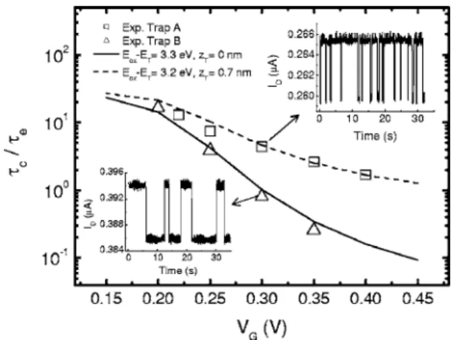
dis-tributione is given in Fig. 1 against gate voltage for two
devices labeled Traps A and B. The inset of Fig. 1 shows the corresponding time evolutions of RTS drain current at a cer-tain gate voltage. Figure 1 reveals that while initially the
c/eratio is comparable between Traps A and B, with gate
voltage increasing further, the Trap B’s c/e drops with a
faster rate than Trap A.
III. ANALYSIS AND PHYSICAL INTERPRETATIONS
The size of the trap under study must be significantly less than the oxide thickness used共1.7 nm兲 since no noticeable change in the gate current was observed. Hence, the trap responsible for the measured RTS in drain current is a nanometer-scale trap. To explore the measured c/e, it is
necessary to know in advance the amount of the image or
PHYSICAL REVIEW B 72, 235417共2005兲
induced charge on the gate as a single electron is inserted into the oxide trap. First of all, it is well recognized that once a single electron is inserted into the oxide, the Debye screen-ing length of a sscreen-ingle electron 共⬃70 nm兲 共Refs. 4 and 6兲 develops laterally around a negatively charged nanometer-scale trap in the oxide. Here, the Debye screening length is the effective size of the “cloud” of the induced charges on the electrodes. Thus, only within the Debye screening length can the plate capacitor approximation readily apply, leading to a capacitive coupling equivalent circuit as shown in Fig. 2. The capacitance model accounts for the effect of the trap depth and the charge sharing between gate, inversion layer, and silicon depletion region. Owing to the insertion of one electron into a depth zTfrom the SiO2/ Si interface, the gate
oxide capacitance per unit area Coxassociated with the oxide
thickness toxcan be separated into two distinct components: the trap to anode 共near the gate兲 capacitance per unit area Cg= Coxtox/共tox− zT兲 and the trap to cathode 共near the
chan-nel兲 capacitance per unit area Cc= Coxtox/ zT. The other
ca-pacitances such as the inversion-layer capacitance per unit area Cinv and the silicon depletion capacitance per unit area
Cdep can be quantified using a self-consistent Schrödinger-Poisson equations solver with the process parameters men-tioned above as input. Figure 3 shows the simulated results
of the key capacitance components versus gate voltage. The proposed capacitance model exactly reduces to that by Schulz1 for the case of z
T= 0. Indeed, the calculated results
on a 17-nm oxide are consistent with those in the literature.2
While a single electron is inserted into the trap, the po-tential change ⌬V in the trap reads as ⌬V=q/共ADB⫻Ceff兲 where ADBis the effective Debye screening area and Ceff, the equivalent capacitance per unit area seen from the trap to the ground, can be derived from the model. Then the image charge共positive兲 QGdeveloped on the gate electrode can be
expressed as QG=⌬V⫻共ADB⫻Cg兲. Combining both equa-tions while eliminating the common factor 共i.e., Debye screening area兲, one achieves QG共=qCg/ Ceff兲
QG= q⫻
zT⫻ 共Cinv+ Cdep兲 + Coxtox
toxCox+ tox共Cinv+ Cdep兲
. 共1兲
The calculated gate image charge as depicted in Fig. 4 re-mains constant until a 2DEG 共2D electron gas兲 layer criti-cally appears 共at VG⬇0.1 V兲, and then due to increasing
screening by the inversion-layer charge, the gate image charge decreases with increasing gate voltage. Specifically, the figure reveals that an increase in the trap depth can sub-stantially increase the gate image charge. In the presence of a 2DEG layer, the source and drain are electrically tied
to-FIG. 1. Measured mean capture time to mean emission time ratio versus gate voltage for two devices labeled Traps A and B. The inset shows the time records of RTS drain current at a fixed gate voltage of 0.3 V. The fitting lines from Eq.共2兲 are also shown.
FIG. 2. Capacitive coupling equivalent circuit, accounting for the effect of the trap depth and the charge sharing between gate, inversion layer, and silicon depletion region.
FIG. 3. Simulated results of the key capacitance components versus gate voltage.
FIG. 4. Calculated gate image charge and Coulomb energy ver-sus gate voltage for two trap depths in the oxide.
M.-P. LU AND M.-J. CHEN PHYSICAL REVIEW B 72, 235417共2005兲
gether and thereby the Coulomb energy can readily be writ-ten as⌬E⬇QGVG.1,2The calculated Coulomb energy is
to-gether plotted in Fig. 4, showing that the Coulomb energy associated with the interface trap increases with gate voltage until encountering a certain peak. However, such a peak point disappears in the case of nonzero trap depth and the Coulomb energy instead piles up over the conventional value.
According to the principle of detailed balance with the Coulomb energy included, thec/eratio can read as1
c
e
= e共ET−EF+⌬E兲/kBT. 共2兲
In Eq. 共2兲, the trap level ET relative to the quasi-Fermi
level EF is a function of gate voltage and can readily be quantified using the Schrödinger-Poisson solver. The best fitting results achieved using Eq. 共2兲, with zT= 0.7 nm
and EOX− ET= 3.2 eV for Trap A and zT= 0 nm and
EOX− ET= 3.3 eV for Trap B, are shown in Fig. 1. Here EOX
denotes the oxide conduction band edge. Evidently, the fit-ting quality is fairly good. The extracted EOX− ETvalues are
close to the SiO2/ Si interface barrier height, as expected due
to the low voltage operation. It is hence argued that an inter-face trap exists in the Trap B device while a 0.7-nm deep trap in the oxide prevails in Trap A. In other words, the conven-tional Coulomb energy appears to work well for the Trap B device but leads to poor quality in fitting the Trap A data. Such a remarkable difference inc/ebetween Traps A and B
can therefore serve as experimental evidence of the Coulomb energy enhancement.
Other corroborating evidence can be obtained through the fitting of the measured mean capture time versus gate voltage as shown in Fig. 5. Since the capture kinetics involve the thermal activation process at room temperature of operation, a multiphonon emission theory was utilized to calculate the capture time 1 c =th ns zqm e−⌬E/kBT 共3兲
wherethis the carrier thermal velocity共⬇1.23⫻105 m / s兲,
ns is the inversion-layer electron density per unit area, and
zqm is the average thickness of the inversion layer. is the
multiphonon capture cross section and can be written as
=0e−EB/共kB⫻T兲. 共4兲
The prefactor 0 involves the interaction between the trap
state and free electron wave function.EB is the thermal
acti-vation barrier height and according to multiphonon emission theory the thermal activation barrier height at high tempera-ture共kBT⬎ប/ 2兲 can reduce to12,13
EB=
共E0− ET− Sប兲2
4Sប , 共5兲
where E0 is the energy level of the lowest subband for
unprimed valley and Sបis the lattice relaxation energy共S is the Huang-Rhys factor兲. Fitting thecdata in Fig. 5 to Eq.
共3兲 yielded the lattice relaxation energy Sបof 1.2 and 0.025 eV for Traps A and B, respectively; and 0 of 2.03⫻10−23
and 3.66⫻10−22m2 for Traps A and B, respectively. The
fitting quality is again good and the same parameters readily reproduced theedata as depicted in Fig. 5. Specifically, the
extracted0values are physically reasonable from the
view-point of the penetration of the wave function into the oxide: the capture cross section decreases with increasing trap depth from the SiO2/ Si interface. The extracted values of the
lat-tice relaxation energy also correctly reflect the status of the trap: A deeper trap共i.e., Trap A in our work兲 is accompanied with a higher lattice relaxation energy.14,15Using the above
extracted results, we constructed a configuration coordinate diagram of the underlying electron-lattice system as sche-matically shown in Fig. 6 for both devices. Also plotted in Fig. 6 are the MOS energy band diagrams 共removing the polysilicon part兲 in the flatband case, showing the spatial
FIG. 5. Comparison of the measured and calculated capture time constants and emission time constants versus gate voltage.
FIG. 6. Schematic configuration coordinate diagrams used for a phenomenological description of the capture and emission kinetics encountered in Traps A and B. The corresponding energy band dia-grams in flatband conditions are also given, schematically showing the trap depth and its energetic level in the oxide.
OXIDE-TRAP-ENHANCED COULOMB ENERGY IN A… PHYSICAL REVIEW B 72, 235417共2005兲