1976 EEE TRANSACTIONS ON MAGNETICS, VOL. 29, NO. 2, MARCH 1993
A 3-Dimensional Analysis of Electrooptic Modulators
by the Method of Lines
Shyh- Jong Chung
Institute of Communication Eng., National Chiao Tung University Hsinchu, Taiwan, R.O.C.
Abstract-A 3-dimensional analysis using the method of lines is developed to study the electrostatic field within an electrooptic switch/modulator. The effect of the ends of the electrodes is investigated by consid- ering the distributions of the electric field along the transverse and longitudinal directions. Also, the ca- pacitance related to the abrupt ends is calculated for several parameters of the structure.
I. INTRODUCTION
Electrooptic (EO) modulators are widely used in inte- grated optical circuits or electrooptic integrated circuits as a connection between optical and electrical signals [1]- [3]. They are also used in microwave circuits [4]. In these devices, a controlling electric field is applied to the sub- strate to perturb the permittivity of the guiding medium through the electrooptic (Pockel) effect, achieving modu- lation of the guided optical wave. The depth of the mod- ulation relies both on the overlap integral factor [5] and the length of the modulator.
Many authors have paid their attentions to the anal- ysis of the field distribution near the electrodes of the EO modulators, with approaches such as comformal map- ping [6]-[8], the method of lines [9], finite element method [10][11], and point-matching method [l2][13]. For simplic- ity the end effects of electrodes are ignored so that a two- dimensional problem is tackled in their analysis. How- ever, for a modulator operated under several GHz, the electrode lengths are much smaller than the wavelength. It seems that a three-dimensional analysis is needed to get more complete informations about the electric fields in the modulators.
In this study the author implements a static analysis of EO modulators using a 3-dimensional method of lines, with special emphasis on the end effect of the electrodes. Section I1 describes the method of the analysis. Since the
Manuscript received May 28,1992. This work was supported by the National Science Council of the Republic of China under Grant NSC 81-0404-E-009-529.
method of lines is well-documented in [14], only a brief summary is given. Section I11 discusses some numerical results followed by conclusions in section IV.
11. ANALYSIS
The structure of the EO modulator for analysis is shown in Fig. 1, where two infinitely thin electrodes are placed on a buffer layer Sios which in turn adheres to an anisotropic material LiNbOs. Since the change in dielectric constant of LiNbOB due to Ti diffusion used in fabricating the waveguides is rather small, its effect is neglected in the analysis. The whole structure is enclosed by perfect elec- tric conductors (PEC) except at the side of z = -L where
a perfect magnetic conductor (PMC) is introduced either due to the symmetry of the geometry or due to the invari- ances (in the z direction) of the field and charge distribu- tions at z
<
-L. By noting that the dimensions of the structure are very small compared to the operating wave- length, an electrostatic approach is used in the following analysis.Y P M C
x
Fig.1. Structure for analysis.
EEE TRANSACTIONS ON MAGNETICS, VOL. 29, NO. 2, MARCH 1993
Let E ( x , y , z ) and 4 ( x , y 1 z ) be the electric field and potential distributions, respectively. Then
E = - V 4
,
(1)and 4 ( x , y , z ) , in each layer, is a solution of the Laplace equation :
Here the relative permittivity tensor of the layer of LiNbOs is assumed to be diagonal. Note that in the re- gions of air and Si02, the materials are isotropic so that €r, = €ry
=
€r,.The boundary conditions (B.C.) subjected to ( 2 ) are : 1) At the enclosure walls :
4 = 0
,
for PEC ;,
for PMC.
--
a4
8%
-O2 ) At the interface between Si02 and LiNbOs :
4
and cry% both be continuous.3) At the interface between Si02 and air (y = 0) :
4
be continuous and equal to the potential vkapplied to the k-th electrode, k=1,2 ;
Where p ( x , z ) represents the charge distribution on the plane of y = 0, which is zero outside the electrode region, and to is the permittivity of the free space. The super- script ” - ” and
”+
” mean the lower and upper sides ofthe interface, respectively.
Equation ( 2 ) is solved by the method of lines [14]. First by further considering the symmetry of the structure in the x direction (let VI
=
-V2= V ) ,
a PEC wall is placedat the plane of x = A / 2 to simply the analysis. In the implementation of the method of lines, a finite difference procedure is used in the 5 and z directions to handle the derivatives in ( 2 ) . Fig. 2 shows the top view of the re- duced structure and the locations of the so-called ”e-lines” and ”h-lines”. The potential and its second derivative are evaluated on the e-lines and the first derivative of the potential is evaluated on the h-lines. To reduce the num- ber of variables, the lines near the end of the electrode are denser than those elsewhere by recognizing that the potential has the most variety near the end. Note that e-lines (h-lines) should be put aIong the PEC (PMC) and the values on these lines are set to be zeros by B.C. 1.
Following the procedures decribed in [14], a set of cou- pled differential equation is derived after discretizing ( 2 )
a-
-
0 0 0 0 0 0 0 0 0 0 0 0 0 0 0 0 0 0 0 0 0 0 0 0 0 0PEC
I
L!
0e-line
oh-line
Fig.2. Top view of the reduced structure showing the locations of e-lines and h-lines.
in the x and z directions. By introducing the diagonal eigenvalue matrix A: (A:) and the orthogonal eigenvector matrix T belonging to the difference operator
P, (P8),
these equations can be decoupled to
In (3), I is the unit matrix, h, (h,) is the average distance between two adjacent e-lines in the x ( 2 ) direction, and
&
is the potential distribution, which is given by6
=T’”@
1 (4)with superscript
” t
” denoting the matrix transpose and@ representing the potential vector calculated on the e- lines.
The general solution for the i-th component of
8
can be found asBy imposing B.C. 2 ) and 3 ) on ( 5 ) , an inhomogeneous matrix equation is obtained
where
p
represents the transformed charge distribution on the interface of y = 0. After transforming back to the spatial domain, and recognizing that charges exist only1978 IEEE TRANSACTIONS ON MAGNETICS, VOL. 29, NO. 2, MARCH 1993
on the electrode and that the electrode potential is equal to V , a reduced matrix can be obtained
Z'pel= @e1 1 (8)
where the subscript " e l " denotes that the vectors contain
only the elements on the e-lines crossing the electrode. Oel is a constant vector whose elements are equal to V.
Eq. (8) is inverted to get the charge distribution on the electrode, the potential and electric field are then obtained from (71, (51, (41, and (1).
111.
RESULTS
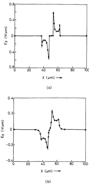
As a check of the validity of the computer program, Fig. 3 (a) and (b) show the normal electric fields
(Ey)
of the present approach, which are scanned at z = -80pm,compared with those obtained by the two-dimensional point matching method [12]. In this illustration the bot- tom LiNbO3 layer is replaced by Si02 for the purpose of comparison. The electric fields are expected to reach the stable values at z = -80pm, namely, the results should be
equal to those calculated from two-dimensional approach. The close agreements of the curves in Fig. 3 verify the validity of the present analysis.
In the following discussions, the relative permittivity for the y-cut LiNbOs is set to be ( c r c = E r Z = 43, cry = 28),
and that for Si02 is (erz = cry = crz = 3.8). The thick- nesses of the layers of LiNbO3 ( H I ) and air (H3) are both chosen to be lmm. The width (W) and the imposed potential (V) for the electrode are 10pm and 1 V, re- spectively. The length parameters
D ,
L , and Gs defined in Fig. 1 are 100,100, and 37.5pm1 respectively. Under the selections of these length parameters, the influence of the side walls (PEC, PMC) on the field behaviors can be neglected. In the discretization, 16 (15) equally spaced e- (h-) lines are located in the x direction acrossing the electrode range (Gs<
2< Gs
+
W ) . Outside this range,40 6o loo the distance between two adjacent e-line and h-line in- X (m)- creases geometrically with a ratio of 1.1. The same ratio is used in the z direction to space the e-lines and h-lines away from the electrode end. Under this discretization, the CPU time for obtaining numerical data from a given structure is about 3 minutes in the VAX-8800 computer. Fig. 4 shows the normal electric fields
(Ey)
at the plane of y = -H, for z= +20,0,-20,
and -80pm. The field at the position 20pm-ahead-of the electrode end ( z = +20pm) is negligible. Note that the shapes of the three curves for .z = 0, -20, and -80pm are similar, and that the field behavior at z = -20pm is the same as that at z = -80pm, which means that the end effect can be neglected as the observation point is 20pm away from the end. 0.8 0 O a 4 " (a) 0.4 0.2 0 (b)Fig.3. Distributions of the normal electric fields (Ey) along the lines (a) (y = 0 , z = -80pm) and (b) (y = - 0 . 7 5 p m , z = - 8 0 p m ) . The bottom LiNbO3 layer is replaced by Si02 (Crz = cry = crZ = 3.8).
-
present analysis; o o o results from [12].Fig. 5 illustrates the distributions of
Ey
in the z di- rection near the inner edge of one of the electrodes (z=
Gs
+
W-
0.16pm), calculated at the plane of y = -H;.The field is almost zero outside the electrode. For the case of no buffer layer (Hz = Opm), the field approaches
infinity when the observation point moves along the elec- trode and toward its end, which is a consequence of the edge condition.
The capacitance, AC, associated with the abrupt stop of the electrodes can be calculated from the difference between the total charge,
Qlotl
and the charge per unit length of infinitely long electrodes, &awe, asIEEE TRANSACTIONS ON MAGNETICS, VOL. 29, NO. 2, MARCH 1993 1979
1
0.2-
E Y. \2
0 - >r w - 0 . 2 --
0.41 I I I IJ
0 20 40 60 80 100 X (pm)-Fig.4. Normal electric fields (E,) at the plane of y = -HF for
I = +20,0,-20, and -80pm. H2 = 0.2pm.
1
I I0 -40 -80
c-
2
( p m )Fig.5. Distributions of the normal electric field (E,) along the line (z = Ga
+
W-
0.16pm,y = -HT) for Hz = 0, 0.2, and 0.5pm. whereA V
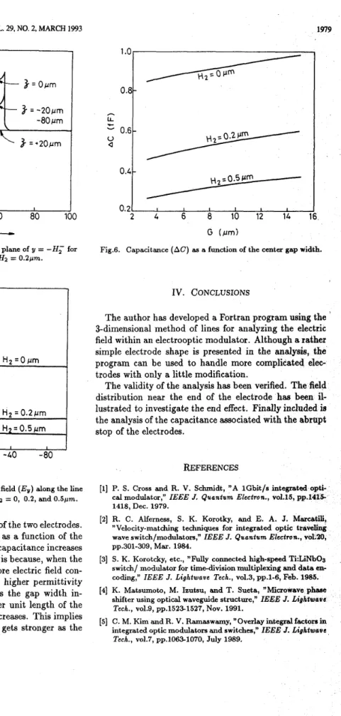
is the potential difference of the two electrodes.Fig. 6 shows the capacitance AC as a function of the gap width G. For a given width, the capacitance increases a8 the buffer layer gets thinner. This is because, when the thickness of the buffer decreases, more electric field con- centrates at LiNbOs which has the higher permittivity than the buffer SiOz. Note that as the gap width in- creases, although the capacitance per unit length of the uniform electrodes decreases, AC increases. This implies that the end effect of the electrodes gets stronger as the gap width increases.
1
.o
LL
O.%
0.21 I I I I 1 1
I
2 4 6 8 10 12 14 16
G (elm)
Fig.6. Capacitance (AC) as a function of the center gap width.
IV. CONCLUSIONS
The author has developed a Fortran program using the '
3-dimensional method of lines for analyzing the electric field within an electrooptic modulator. Although a rather simple electrode shape is presented in the an
program can be used to handle more complicated elec- trodes with only a little modification.
The validity of the analysis has been verified. The field distribution near the end of the electrode has
b
lustrated to investigate the end effect. Finally incl the analysis of the capacitance associated with the stop of the electrodes.
REFERENCES
[I] P. S. Cross and R. V. Schmidt, "A lGbit/s integrated cal modulator," IEEE J. Quantum Electron., ~01.15, 1418, Dec. 1979.
"Velocity-matching techniques for integrated optic wave switch/modulators," IEEE J . Quantum Electro [2] R. C. Alferness, S. K. Korotky, and E. A. J.
pp.301-309, Mar. 1984.
[3] S. K. Korotcky, etc., "Fully connected high-speed Ti:LiNbOs switch/ modulator for time-division multiplexing and data en- coding," IEEE J . Lightwave Tech., vo1.3, pp.1-6, Feb. 1985. shifter using optical waveguide structure," IEEE J. Light Tech., vo1.9, pp.1523-1527, Nov. 1991.
[5] C. M. Kim and R. V. Ramaswamy, "Overlay integral factors in integrated optic modulators and switches," IEEE J. Lighiwave
Tech., vo1.7, pp.1063-1070, July 1989.
1980 IEEE TRANSACTIONS ON MAGNETICS, VOL. 29, NO. 2, MARCH 1993
[6] 0. G. h e r , "Integrated optic electrooptic modulator elec- trode analysis," IEEE J. Quantum Electron., ~01.18, pp.386- 392, Mar.1982.
[7] J. S. Wei, "Distributed capacitance of planar electrodes in o p tic andacoustic surface wave devices," IEEE J. Quantum Elec-
iron., vo1.13, pp.152-158, Apr. 1977.
[8] D. Marcuse, "Optimal electrode design for integrated optics modulators," IEEE J. Quantum Electron., ~01.18, pp.393-398, Mar. 1982.
[9] A. G. Keen, M. J. Wale, M. I. Sobhy, and A. J. Holden, "Quasi- static analysis of electrooptic modulators by the method of lines," IEEE J. Lightwave Tech., vo1.8, pp.42-50, Jan. 1990. [lo] R. V. Mustacich, "Scalar finite element analysis of electrooptic
modulation in diffused channel waveguides and poled wave- guides in polymer thin films," Applied Optics, ~01.27, pp.3732-
3737, Sept. 1988.
[I11 J. C. Yi, S. H. Kim, and S. S. Choi, "Finite-element method for the impedance analysis of traveling-wave modulators," IEEE
J. Lightwave Tech., vo1.8, pp.817-822, June 1990.
[12] D. Marcuse, "Electrostatic field of coplanar lines computed with the point matching method," IEEE J. Quantum Elec- tron., vo1.25, pp.939-947, May 1989.
[13] H. Jin, R. Vahldieck, M. Bdlanger, and Z. Jacubczyk, "A mode projecting method for the quasi-static analysis of electrooptic device electrodes considering finite metalization thickness and anisotropic substrate," IEEE J. Quantum Electron., ~01.27, pp.2306-2314, Oct.,1991.
[14] R. Pregla and W. Pascher, "The Method of Lines," Ch.6, in Numerical Techniques for Microwave and Millimeter- Wave Passive Structures, ed. by T.Itoh, New York Johnwiley, 1989.