epitaxy
K. M. Chen, H. J. Huang, C. Y. Chang, L. P. Chen, and G. W. Huang
Citation: Journal of Vacuum Science & Technology A 18, 1196 (2000); doi: 10.1116/1.582324
View online: http://dx.doi.org/10.1116/1.582324
View Table of Contents: http://scitation.aip.org/content/avs/journal/jvsta/18/4?ver=pdfcov
Published by the AVS: Science & Technology of Materials, Interfaces, and Processing
Articles you may be interested in
Ultrathin low temperature SiGe buffer for the growth of high quality Ge epilayer on Si(100) by ultrahigh vacuum chemical vapor deposition
Appl. Phys. Lett. 90, 092108 (2007); 10.1063/1.2709993
Growth and characterization of ultrahigh vacuum/chemical vapor deposition SiGe epitaxial layers on bulk single-crystal SiGe and Si substrates
J. Vac. Sci. Technol. A 20, 1120 (2002); 10.1116/1.1464840
n- Si /i-p-i SiGe /n- Si structure for SiGe microwave power heterojunction bipolar transistor grown by ultra-high-vacuum chemical molecular epitaxy
J. Appl. Phys. 86, 1463 (1999); 10.1063/1.370913
Study of thin film deposition processes employing variable kinetic energy, highly collimated neutral molecular beams
J. Vac. Sci. Technol. A 16, 3423 (1998); 10.1116/1.581497
Controlling threading dislocation densities in Ge on Si using graded SiGe layers and chemical-mechanical polishing
Deposition of polycrystalline Si and SiGe by ultra-high vacuum chemical
molecular epitaxy
K. M. Chen,a)H. J. Huang, and C. Y. Chang
Department of Electronics Engineering and Institute of Electronics, National Chiao-Tung University, Hsin-Chu, Taiwan 300 Republic of China
L. P. Chen and G. W. Huang
National Nano Device Laboratory, Hsin-Chu, Taiwan 300 Republic of China 共Received 20 August 1999; accepted 7 February 2000兲
The polycrystalline Si1⫺xGex 共poly-Si1⫺xGex兲 films have better properties than poly-Si for device
fabrications, such as lower proceeding temperature and process thermal budget. For these reasons, the poly-Si1⫺xGexfilms have been utilized for low-temperature thin film transistor fabrications and
gate electrodes of metal–oxide–semiconductor transistors. In this work, disilane and germane were used to grow poly-Si1⫺xGex films at low temperature 共⬍600 °C兲 by the cold-wall type ultrahigh
vacuum chemical molecular epitaxy system. The poly-Si1⫺xGexfilms were deposited on oxide and
nitride surfaces. The Ge fraction x was evaluated from x-ray diffraction and Auger electron spectroscopy. It is observed that the Ge fraction increases with the increase of the GeH4flow rate. The result is only slightly related to the substrate type. The growth rate increases with the Ge fraction at lower values and then decreases with the Ge fraction in the higher composition range. This implies that the growth mechanism of poly-Si1⫺xGexfilms is different from that of epitaxial
Si1⫺xGex on Si. The uniformity of poly-Si1⫺xGex films depends on the Ge fraction, and it is
improved by the addition of germanium. The result can be explained by the lower activation energy 共⬍0.25 eV兲 of poly-Si1⫺xGex deposition as compared to that of poly-Si共⬃2.1 eV兲. From the x-ray
diffraction and atomic force microscopy analyses, the crystallinity and surface roughness of films are suitable for device fabrications. © 2000 American Vacuum Society.关S0734-2101共00兲07704-6兴
I. INTRODUCTION
Polycrystalline silicon–germanium 共poly-Si1⫺xGex兲 has recently been shown to be a favorable alternative to poly-crystalline silicon 共poly-Si兲 for various applications in inte-grated circuit共IC兲 technologies.1–5Since the melting point of Si1⫺xGex is lower than that of Si, the fabrication processes
such as deposition, crystallization, and dopant activation oc-cur at lower temperatures for Si1⫺xGex than for Si. In
addi-tion, poly-Si1⫺xGex films with Ge mole fractions up to 0.6
are compatible with mature Si technologies. Poly-Si1⫺xGex
films have been utilized for the low temperature thin film transistor 共TFT兲 fabrications without exceeding 550 °C,1 whereas comparable TFTs fabricated in poly-Si require pro-ceeding temperatures at or above 600 °C. The significant re-ductions in process temperature afforded by poly-Si1⫺xGex
make it a promising material for TFT IC applications. Fur-thermore, with lower resistivity and variable work function, the heavily doped p-type poly-Si1⫺xGex is an interesting
gate-electrode material for submicrometer complimentary metal–oxide–semiconductor technologies.2–5 The work function of P⫹poly-Si1⫺xGexdecreases with increasing Ge
mole fraction x, so that the threshold voltage can be adjusted simply by varying the Ge content inside the films.3This al-lows one to reduce the surface channel doping while retain-ing the same threshold voltage as for poly-Si gate. This result increases the current drivability, the transconductance, and
decreases the subthreshold swing of the transistor.4Since the higher dopant activation rate and lower diffusivity of boron atoms in poly-Si1⫺xGex film are compared to poly-Si films,
the boron penetration and poly-gate depletion effect can be reduced for poly-Si1⫺xGex gated metal–oxide–
semiconductor field effect transistors 共MOSFETs兲.5 Finally, poly-Si1⫺xGexcan be used as local interconnects when
effi-cient activation of carriers with suppression of diffusion is required.
Among the published reports, poly-Si1⫺xGexfilm can be
formed by conventional low-pressure chemical vapor depo-sition共LPCVD兲,6–9the rapid thermal LPCVD,10,11and ultra-high vacuum 共UHV兲 CVD systems.12,13 Deposition of poly-Si films at reduced pressures 共⬍10 mTorr兲 has been investigated to achieve low temperature processing.14–16 It has been found that the transition temperature for an as-deposited Si film from a polycrystalline to an amorphous state is dependent on the growth pressure, and is significantly lowered at reduced pressures.14 In a previous report, the poly-Si1⫺xGex with a fine grain structure has been
demon-strated at temperatures as low as 500 °C using
UHVCVD.12–17Therefore, UHVCVD shows the most prom-ising method for low-temperature poly-Si film deposition.
In this article, the deposition of undoped poly-Si1⫺xGex
films onto SiO2 and Si3N4 in a UHV chemical molecular epitaxy 共UHVCME兲 system is described. This UHVCME system features a cold-wall reactor with an extremely low base pressure (⬃10⫺10Torr) as well as the reduced deposi-tion pressures 共⬍1 mTorr兲. These conditions allow
ex-a兲Author to whom correspondence should be addressed; electronic mail:
tremely low temperature共below 550 °C兲 Si/Si1⫺xGex
epitax-ial growth to proceed on the Si substrate.18,19 The dependence of the Ge fraction and growth rate on the Si2H6 and GeH4 flow rates are evaluated from x-ray diffraction 共XRD兲 and surface profile measuring system, respectively. The growth mechanisms of poly-Si and poly-Si1⫺xGexhave
been discussed and compared with that of epitaxial Si/Si1⫺xGex. The surface morphology and structure proper-ties of these films are also presented.
II. EXPERIMENT
The UHVCME system used in this study includes a water-cooled cold wall stainless steel growth chamber, a loading chamber, separate nozzles for process gases, and a computer-controlled gas switching box. A schematic draw-ing of this system is shown in Fig. 1. The growth chamber is pumped by a 1000
l
/s turbomolecular pump and a base pressure of 2⫻10⫺10Torr can be obtained. The chamber pressure is also maintained below 1⫻10⫺3Torr during the deposition process by this pump. The wafers were loaded into the loading chamber and then the chamber was pumped down to 10⫺6Torr as soon as possible. After the wafers were transferred into the growth chamber for deposition, the heater was lowered and started to heat the wafer to the depo-sition temperature at a ramp of 150 °C/min. Source gases are pure disilane from 1 to 10 sccm and pure germane from 1 to 10 sccm. The flow rates of reaction gases are controlled pre-cisely by their own mass-flow controllers. In this work, 6 in. 共100兲 Si wafers coated with a thermal oxide or nitride were used as the substrates. Prior to deposition, the substrates were cleaned using the standard RCA cleaning procedure. With this treatment, the wafers were subjected to a 5:1:0.25 H2O:H2O2:NH4OH bath at 75 °C for 10 min, followed by a 10 min rinse in de-ionized 共DI兲 water, and then to a 5:1:1 H2O:H2O2:HCl bath at 75 °C for 10 min, followed by a 10 min rinse in DI water and spin dry.The thicknesses of the deposited films were determined by using a masked etch and measuring the step height using a surface profile measuring system with an accuracy within 20 nm. The Ge fraction of the deposited poly-Si1⫺xGexfilms was primarily evaluated by XRD. To verify the accuracy of the XRD method, Auger electron spectroscopy 共AES兲 was also performed to determine the Ge fraction with careful calibration. Atomic force microscopy was used to investigate the surface morphology of the deposited films.
III. RESULTS AND DISCUSSIONS
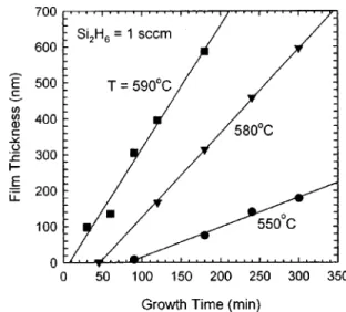
Figure 2 shows a typical plot of thickness measurement as a function of growth time for the poly-Si films deposition on SiO2at different temperatures. The slope of the fit line and its intercept with the x axis are defined as the growth rate and the incubation time, respectively, for each growth tempera-ture. As illustrated, the poly-Si nucleation on an insulating substrate did not begin immediately, and there was an initial short period during which the poly-Si was not observed on insulating substrate by scanning electron microscopy共SEM兲. It is clearly noted that the growth rate increases while the incubation time decreases with increasing growth tempera-ture. The increase of incubation time with decreasing growth temperature is due to slower nucleation and growth rates at lower temperatures.17 Figure 3 shows the incubation time of poly-Si1⫺xGex films grown at 550 °C for thermal oxide and
nitride substrate as a function of the GeH4 flow rate. With oxide substrate, a considerable amount of the incubation time is due to the rather low deposition rate 共⬃0.9 nm/min兲 as well as the low generation rate of the nuclei.17Because of the long incubation time for SiO2 substrate, we found that the poly-Si1⫺xGex film cannot be directly deposited on the gate
oxide for poly-Si1⫺xGexgated MOSFET fabrication, and the
gate oxide was destroyed under the UHV environment. To avoid this problem, a thin nitride layer must be deposited on gate oxide before the poly-Si1⫺xGex growth. With a nitride
substrate, the incubation time was about eight times smaller
FIG. 1. Schematic diagram of the ultra-high vacuum chemical molecular epitaxy共UHVCME兲 system.
FIG. 2. Film thickness vs growth time for poly-Si grown on SiO2at different
growth temperatures. The Si2H6flow rate remained at 1 sccm.
than that of the oxide substrate. This fact suggests that, on a nitride surface, the generation rate of the nuclei is larger than that on an oxide surface. This may be due to either the higher areal density of chemical bonds on the nitride surface, or the chemical difference between oxide and nitride.20 In both cases, we found that the addition of GeH4 increases the in-cubation time. This result may be due to the higher surface mobility of Ge adatoms on the substrate surface which retard the generation of nuclei.
In this study, we found that the substrate type did not affect the Ge fraction and growth rate of the poly-Si1⫺xGex
films. Figure 4 is an Arrhenius plot of deposition rates versus reciprocal of the growth temperatures. The activation energy associated with pure poly-Si growth was found to be about 2.1 eV. This value is the same as the activation energy of Si epitaxy with the UHVCME system. The growth of poly-Si follows an identical mechanism of Si epitaxy on the共100兲 Si surface. The activation energy for the Si growth rate
corre-sponds to the energy required for hydrogen atoms to desorb from the Si共100兲 surface.21This is evidence that the Si depo-sition rate is controlled by the desorption rate of hydrogen from the substrate surface. When GeH4was added, the poly-Si1⫺xGexgrowth rate was enhanced in the low temperature
range 共⬍550 °C兲 and the activation energy was reduced to 1.5 eV for GeH4⫽1.5 sccm. The decrease in activation en-ergy with the addition of a small fraction of GeH4is consis-tent with work on Si1⫺xGexepitaxy.
18
This phenomenon was also observed by the LPCVD system,8and we speculate that Ge atoms at the growth interface serve as hydrogen desorp-tion centers and reduce the activadesorp-tion energy for hydrogen desorption.22 As the deposition temperature increases, the curves show lower apparent activation energy less than 0.25 eV. This indicates that the deposition changes from the reaction-rate limited regime to the mass-transport limited re-gime. Since the chemical surface reaction rate increases rap-idly with the addition of GeH4, the reactant gas supply reaching the substrate surface cannot keep up with the de-mand of the reaction. Therefore, the transition temperature between the reaction-rate limited regime and mass-transport limited regime decreases with increasing GeH4 fraction in the reaction gas.
The XRD spectra of the poly-Si1⫺xGex with x⫽0.08,
0.21, and 0.36 are shown in Fig. 5. Peaks corresponding to the 共111兲, 共220兲, and 共311兲 planes are indicators of diamond crystal structure. All the films show preferential orientation of the 共111兲 plane in spite of Ge fraction. The full width at the half maximum of the XRD peak for the 共111兲 plane is around 0.3°, indicating that the crystallinity of film is good enough compared with typical poly-Si film deposited by LPCVD. The locations of the singular peaks are located in between those of poly-Si and poly-Ge, and are shifted more toward those of pure Ge for the films with higher Ge frac-tion. The increase in the Ge fraction results in an increase in the lattice constant. The lattice constant was determined by the average of the lattice constants obtained from the 共111兲 and共220兲 peaks. The lattice constants were used to calculate
FIG. 3. Incubation time for poly-Si1⫺xGexfilms deposited at 550 °C as a
function of GeH4flow rate.
FIG. 4. Film deposition rate as a function of the inverse of deposition tem-perature for various GeH4flow rates.
FIG. 5. X-ray diffraction data for 200 nm thick poly-Si1⫺xGexfilms
depos-ited at 580 °C.
the Ge atomic fraction x by Vegard’s law. Because the strain of grain is present in the as-deposited poly-Si1⫺xGex films,
the lattice distortion exists and affects the precision of mea-surement. To obtain the measurement uncertainty of the XRD method, some samples were measured by AES. The AES data have been calibrated with Si and Ge standards. Compared with AES analyses, the accuracy of the Ge frac-tion determined by XRD is within 2 at. %. Figure 6 shows the dependence of the Ge fraction x on the GeH4flow rate. The Si2H6 flow rate was kept at 1 sccm. The Ge fraction increased monotonically with the increase of the GeH4flow when the growth temperature remained constant. The Ge fraction increases slightly with the decrease of growth tem-perature for fixed Si2H6and GeH4flow rates. This observa-tion is consistent with previous findings of lower activaobserva-tion energies for germanium deposition compared to those for silicon deposition.23
Poly-Si1⫺xGex deposition rate is plotted as a function of the Ge atomic fraction in Fig. 7. Each line represents a con-stant deposition temperature. The growth rate increases with the Ge fraction at lower values and then decreases with the Ge fraction in the higher composition range. The variation of the deposition rate for poly- Si1⫺xGexfilms with Ge fraction
is significantly different from that of epitaxial ones.19 This phenomenon was also observed by other UHVCVD system and was explained by the different strain energy contained in the poly- Si1⫺xGexand epitaxial Si1⫺xGex.13 To obtain
fur-ther insight into the above results, we divided the Si1⫺xGex
growth rate RSiGeinto the Si growth rate RSiand Ge growth rate RGe, that is, RSiGe is equal to (RSi⫹RGe). The separa-tion was based on the determined Si and Ge fracsepara-tions in the Si1⫺xGex films. Figure 8共a兲 and 8共b兲 show the Si and Ge
growth rates as a function of Ge fraction in the deposited poly-Si1⫺xGex film. For the Si growth rate, a maximum is
observed for each temperature. The Si growth rate increases first, and then decreases with Ge fraction. The Ge growth rate, on the other hand, shows no maximum and increases
with the Ge fraction in the Si1⫺xGexfilm. As observed from
Fig. 4, the deposition is limited by surface reaction at lower Ge fraction. In this case, RSidepends on the Si2H6flow rates, surface reaction rate constants, and the hydrogen desorption rate. Hence the initial increase of RSiat lower Ge fraction is caused by enhancement of hydrogen desorption with Ge in-corporation. When RSiwas increased to a maximum value,
RSi began to decrease with increasing Ge fraction. In the higher composition range, the growth rate is not sensitive to the substrate temperature as illustrated in Fig. 4; this indi-cates that the deposition is controlled by mass transfer. In the mass-transport limited regime, the RSidepends on Si2H6 con-centration, and sticking probability of Si2H6on the Si1⫺xGex
surface. Kim et al.24proposed a model based on the sticking probability of Si and Ge precursors to explain the behavior. They concluded that the decrease of growth rate with in-creasing Ge content in the mass-transport limited regime is due to the sticking probabilities of both Si and Ge precursors being lower on Ge than on Si. In our UHVCME system, we found that the total growth pressure increases linearly with the increase of GeH4 flow rate due to the constant pump speed as shown in Fig. 9. The increase of the growth pres-sure will decrease the gas velocity, and hence the Si2H6 con-centration reaching the Si1⫺xGex surface. This may also be
the reason for the decrease of Si growth rate. However, the actual growth mechanism is not very clear in our UHVCME system, and will be studied in detail in the future. In Fig. 8共a兲, the peaks shift to the left as the deposition temperature increases. This is simply because the reaction rate increases quickly with the deposition temperature, and the deposition enters the mass-transport limited regime at lower Ge frac-tion. In Fig. 8共b兲, RGe increases monotonically with the Ge fraction and almost does not depend on growth temperature. The increase of RGe with Ge fraction is mainly due to the increase of the GeH4 concentration in the bulk gas.
For poly-Si1⫺xGex gated MOSFET application, the
sur-face roughness and thickness uniformity of poly-Si1⫺xGex
FIG. 6. Dependence of Ge fraction on GeH4flow rate with Si2H6⫽1 sccm at
different growth temperatures. FIG. 7. Growth rates of poly-Si1⫺xGexfilms as a function of Ge fraction x at
different growth temperatures.
with nitride substrate were investigated. The maximum peak-to-peak surface roughness and thickness uniformity of poly-Si1⫺xGex films grown on nitride at 580 and 550 °C are
shown in Table I. The surface roughness of poly-Si1⫺xGex
films increases as the GeH4flow rate increased at the same temperature. This is probably because the grain size of poly-crystals becomes larger when the Ge fraction increased. The average grain size was estimated to be 150–180 nm for poly-Si0.79Ge0.21 deposited at 580 °C by SEM measurements. In addition, the smoother films are obtained by lowering the deposition temperature. The thickness uniformity of poly-Si is 16% at 580 °C, and it is undesirable for device application. As observed in Fig. 4, the deposition of poly-Si is limited by surface reaction, so the growth rate of films is strongly de-pendent on the growth temperature. Because the temperature distribution of the substrate heater is not constant, the film thickness is not uniform across the wafer. The thickness uni-formity of poly-Si1⫺xGex films can be improved by the
ad-dition of germanium. As illustrated in Table I, the uniformity
is 2.5% for GeH4⫽1.5 sccm, and reduces to 1.9% for GeH4⫽10 sccm at 580 °C. The deposition of poly-Si1⫺xGex
is limited by mass transfer at 580 and 550 °C. The growth rate tends to become temperature insensitive. For the UH-VCME reactor, an equal flux of reactants to all locations of a wafer surface is supplied, so the thickness uniformity can be improved in the mass-transport limited regime.
IV. CONCLUSIONS
Si2H6 and GeH4 are used to grow poly-Si1⫺xGex by the
cold-wall UHVCME process. The Ge fraction and growth rate of poly-Si1⫺xGex were found to be dependent on the
GeH4 flow rate at a constant Si2H6 flow, while not on the substrate type. The Ge fraction increased monotonically with the increase of GeH4 flow. The Si1⫺xGex growth rates for various Ge fractions were separated into Si growth rate and Ge growth rate. From the results obtained, Si growth rate is greatly enhanced by introduction of a small amount of GeH4, and then decreases when the Ge fraction is further increased. The decrease of growth rate is due to the reduction of the Si2H6 concentration or the sticking probabilities of precur-sors on the Si1⫺xGex surface in mass-transport limited
re-gime. Besides the above effects in Si growth rate, Ge growth
FIG. 8.共a兲 Si and 共b兲 Ge components of poly-Si1⫺xGexdeposition rate vs Ge
fraction x at different growth temperatures.
FIG. 9. Growth chamber pressures of the UHVCME system as a function of the GeH4flow rate during poly-Si1⫺xGexdeposition.
TABLE I. Thickness uniformity and surface roughness of poly-Si1⫺xGex
films at 550 and 580 °C with nitride substrate. The Si2H6flow rate remained
at 1 sccm.
GeH4 共sccm兲
T⫽550 °C T⫽580 °C
Roughness
共%兲 Uniformity共%兲 Roughness共%兲 Uniformity共%兲
0 5.6 14 8.2 16
1.5 9.1 2.6 11 2.5
5 10 2.2 13 2.1
10 11 1.7 15 1.9
rate shows a strong dependence on the GeH4 flow rate. Therefore, the relative variations of the hydrogen desorption rate, source gas concentration, and sticking probability of precursor under different growth conditions are used to ex-plain the above results consistently in this study. The thick-ness uniformity of poly-Si1⫺xGex films depends on the Ge
fraction, and it is improved by the addition of germanium. The result can be explained by the lower activation energy related to deposition of poly-Si1⫺xGex in the mass-transport
regime. In this regime, the Ge fraction and growth rate of poly-Si1⫺xGexare well controlled.
ACKNOWLEDGMENTS
The authors would like to thank Dr. H. C. Lin and C. Y. Lin for experimental assistance. This work was supported by the Republic of China’s National Science Council through Contract No. NSC88-2215-E009-048.
1T.-J. King and K. C. Saraswat, Tech. Dig. Int. Electron Devices Meet.
567共1991兲.
2
T.-J. King, J. R. Pfiester, J. D. Shott, J. P. MccVittie, and K. C. Saraswat, Tech. Dig. Int. Electron Devices Meet. 253共1990兲.
3P.-E. Hellberg, S.-L. Zhang, and C. S. Petersson, IEEE Electron Device
Lett. 18, 456共1997兲.
4
Y. V. Ponomarev, C. Salm, J. Schmitz, P. H. Woerlee, P. A. Stolk, and D. J. Gravesteijn, Tech. Dig. Int. Electron Devices Meet. 829共1997兲.
5W. C. Lee, T.-J. King, and C. Hu, IEEE Electron Device Lett. 20, 9
共1999兲.
6J. Holleman, A. E. T. Kuiper, and J. V. Verweij, J. Electrochem. Soc.
140, 1717共1993兲.
7T.-J. King and K. C. Saraswat, J. Electrochem. Soc. 141, 2235共1994兲. 8
M. Cao, A. Wang, and K. C. Saraswat, J. Electrochem. Soc. 142, 1566 共1995兲.
9N. Kistler and J. Woo, Tech. Dig. Int. Electron Devices Meet. 727共1993兲. 10
M. Sanganeria, D. T. Grider, M. C. Ozturk, and J. J. Wortman, J. Elec-tron. Mater. 21, 614共1992兲.
11K. Shiota, D. Inoue, K. Minami, M. Yamamoto, and J. Hanna, Jpn. J.
Appl. Phys., Part 2 36, L989共1997兲.
12H. C. Lin, T. G. Jung, H. Y. Lin, C. Y. Chang, T. F. Lei, P. J. Wang, R.
C. Deng, J. Lin, and C. Y. Chao, J. Appl. Phys. 74, 5395共1993兲.
13H. C. Lin, C. Y. Chang, W. H. Chen, W. C. Tsai, T. C. Chang, T. G.
Jung, and H. Y. Lin, J. Electrochem. Soc. 141, 2559共1994兲.
14
A. T. Voultsas and M. K. Hatalis, J. Electrochem. Soc. 139, 2659共1992兲.
15D. Meakin, J. Stoemenus, P. Migliorato, and N. A. Economou, J. Appl.
Phys. 61, 5031共1987兲.
16
M. Miyasaka, T. Nakanaza, I. Yudasaka, and H. Ohshima, Jpn. J. Appl. Phys., Part 1 30, 3733共1991兲.
17H. C. Lin, H. Y. Lin, C. Y. Chang, T. F. Lei, P. J. Wang, and C. Y. Chao,
Appl. Phys. Lett. 63, 1351共1993兲.
18G. W. Huang, L. P. Chen, C. T. Chou, K. M. Chen, H. C. Tseng, W. C.
Tsai, and C. Y. Chang, J. Appl. Phys. 81, 205共1997兲.
19L. P. Chen, C. T. Chou, G. W. Huang, W. C. Tsai, and C. Y. Chang,
Appl. Phys. Lett. 67, 3001共1996兲.
20
J. T. Fitch, J. Electrochem. Soc. 141, 1046共1994兲.
21K. Sinniah, M. G. Sherman, L. B. Lewis, W. H. Weinberg, J. T. Yates,
and K. C. Janda, Phys. Rev. Lett. 62, 567共1989兲.
22
M. Stutzmann, R. A. Street, C. C. Tsai, J. B. Boyce, and S. E. Reach, J. Appl. Phys. 66, 569共1989兲.
23T. I. Kamina and D. J. Meyer, Appl. Phys. Lett. 59, 178共1991兲. 24H. Kim, N. Taylor, T. R. Bramblett, and J. E. Greene, J. Appl. Phys. 84,
6372共1998兲.