行政院國家科學委員會專題研究計畫 期中進度報告
子計畫四:OFDM FFT 架構下軟體無線電訊號處理之軟、硬體
輔成設計及其數位通信之應用設計(2/3)
計畫類別: 整合型計畫 計畫編號: NSC92-2220-E-009-021- 執行期間: 92 年 08 月 01 日至 93 年 07 月 31 日 執行單位: 國立交通大學電子工程研究所 計畫主持人: 陳紹基 報告類型: 完整報告 報告附件: 出席國際會議研究心得報告及發表論文 處理方式: 本計畫可公開查詢中 華 民 國 93 年 6 月 1 日
行政院國家科學委員會補助專題研究計畫
期中進度報告
用於軟體無線電基頻處理之系統晶片設計技術-子計畫四:
OFDM FFT 架構下軟體無線電訊號處理之軟、硬體輔成設計及
其數位通信之應用設計(2/3)
計畫類別:□ 個別型計畫 █ 整合型計畫
計畫編號:NSC 92-2220-E -009 -021-
執行期間: 92 年 8 月 1 日至 93 年 7 月 31 日
計畫主持人:陳紹基
共同主持人:
計畫參與人員: 曲建全、陳坤隆、余承穎、 朱元志、吳清泉、賴明秀
成果報告類型(依經費核定清單規定繳交):□精簡報告 █完整報告
本成果報告包括以下應繳交之附件:
□赴國外出差或研習心得報告一份
□赴大陸地區出差或研習心得報告一份
□出席國際學術會議心得報告及發表之論文各一份
□國際合作研究計畫國外研究報告書一份
處理方式:除產學合作研究計畫、提升產業技術及人才培育研究計畫、
列管計畫及下列情形者外,得立即公開查詢
█涉及專利或其他智慧財產權,□一年█二年後可公開查詢 附件一摘要
在這個計劃期中報告中已經得到了五個進展成果。第一個部分是關於可變長度的快速 傅利葉轉換處理器所使用的資料位址產生器設計;另一方面,對於傅利葉轉換中所需要的 旋轉因數指標產生器亦是可變長度快速傅利葉轉換處理器中的重要設計,在這裡共有二個 用於固定基數演算法與一個用於分裂基數演算法的旋轉因數指標產生器設計將會在第二部 分提出。為了減少儲存旋轉因數所佔用的硬體成本,第三部份會介紹一個以遞迴方程式來 產生正弦與餘弦函數的旋轉因數產生器設計。第四部份是一個範例性質的可變長度快速傅 利葉轉換處理器整合實作。最後一部份是一個結合 DCT 技術設計出之一新的高效能之 OFDM 通道估測演算法。Abstract
There are five intermediate results generated so far from our on-going project. All results are targeted on the FFT processor design for the modulation and demodulation of OFDM-based communication systems including DAB, DVB, 802.11a, 802.16 and VDSL systems. The results are: (1) a data address generator designed for memory-based, variable-length FFT processor; (2) three new architectures for coefficient index generation, which can work efficiently with the mentioned variable-length data address generator, where the first two are for fixed-radix FFT algorithms and the third one is for split-radix 2/4 FFT algorithm; (3) a new coefficient generator which can replace conventional high-cost coefficient ROM; (4) a variable-length FFT processor which integrates the advance technologies is proposed in part 4; (5) a high-performance DCT-based channel estimation algorithm for non-sample spaced channel impulse response. 關鍵字:快速傅利葉轉換、位址產生器、係數產生器、正交分頻多工、數位聲訊廣播、數 位視訊廣播。
T
ABLE OFC
ONTENTSABSTRACT... 錯誤! 尚未定義書籤。
1. INTRODUCTION AND PROJECT GOALS... 1
2. DISCUSSION AND RESULTS... 2
2.1 VARIABLE-LENGTH FFT PROCESSOR... 2
2.1.1 Variable-length Data Address Generator ... 2
2.1.2 Variable-length Coefficient Address Generator... 7
2.1.3 Variable-length Processing Element... 8
2.1.4 Variable-length Commutate Mode... 9
2.1.5 The Proposed Variable-length FFT Processor Architecture...11
2.2 CORDIC-BASED PROCESSING ELEMENT OF FFT PROCESSOR... 12
2.2.1 The CORDIC Algorithm and Architecture... 12
2.2.2 The New Angle Decomposition Scheme ... 14
2.2.3 Table reducing scheme ... 15
2.2.4 On-line variable factor compensation... 16
2.2.5 The Overall Operation Flow ... 16
2.2.6 Simulations Results ... 17
3. CONCLUSION ... 18
4. REFERENCES ... 18
1. Introduction and Project Goals
本子計劃主要在於研究多標準之正交分頻調變技術(OFDM)軟體無線電(software defined radio) FFT/IFFT 演算法及架構之設計,考慮其整合性、低功率、快速計算、超大型 積體電路設計實現及其在數位通信之應用設計,特別是數位聲訊廣播(DAB)。FFT/IFFT 運
算為正交分頻調變技術(OFDM) 之核心運算,而 OFDM 為 DAB、DVB、802.11a、
HyperLAN、802.16 等寬頻技術之調變方式。OFDM 也被視為未來 3G 之後之主要之無線通 信技術,而在有線寬頻之非對稱性數位用戶迴路通信技術(ADSL)亦利用相近技術,這兩種 數位通信技術均被視為現在及未來寬頻上網通信之主流技術,有鑑於此多標準、寬頻之廣
大應用及需求,本研究特別著重於多標準之相關於 FFT 信號處理之軟硬體整合設計如:
FFT/IFFT 設計。本計劃將為三年之多年計劃,第一年將著重於現有及未來 OFDM 傳輸理
論、相關應用如DAB、DVB、802.11a、HyperLAN、ADSL 標準之研究及 software defined radio
理論研究,同時也將探討低功率、低複雜度、高速度 FFT/IFFT 演算法之研究及設計,此
外其它相關於FFT 之數位通信應用也將作整體性之探討,如頻域適應性等化、回音消除濾
波器理論與技術,並訂定出 FFT/IFFT 模組之設計規格,此規格將考慮到多標準、多模式
軟體無線電FFT/IFFT 核心模組整合設計。為了配合總計劃及第二子計劃,DAB FFT/IFFT
模組之設計實現亦為主要考量。第二年除了繼續及改善第一年的研究外,將設計出適用數
位信通信應用、及多標準之之FFT/IFFT 架構及電路模組,特別是應用於 DAB OFDM,除
了設計出軟智慧財外(soft IP), 我們也將作模組之 FPGA 實現以驗證設計之正確性,若時
間許可則將 FFT/IFFT 模組委託晶片廠實現之並作驗證。第三年除了繼續及改善第二年之
研究外將開始與其他模組作整合設計及驗證,基本之整合系統仍將以FPGA 實現為主,但
2. Discussion and Results
2.1 Variable-length FFT Processor
In order to realize multi-mode and multi-standard OFDM communication systems, the FFT processor must support length-independent computation and meet the worst-case hardware requirement. Consequently, the FFT processor design must contains an efficient processing element, a variable-length data address generator and a variable-length twiddle factor generator.
2.1.1 Variable-length Data Address Generator
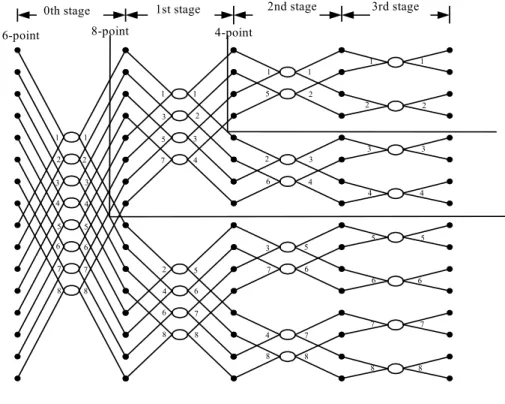
In in-place memory-based FFT processor design, data address generator is decided by the order of butterfly operations. A conventional processing order and control scheme for radix-2 FFT are proposed by Cohen (1976) [1], and the algorithm was then extended and generalized by [2], [3], [4], [5]. However, we can find out that Cohen’s scheme is not suitable for a variable-length FFT when analyzing a sub-segment of signal flow graph for a shorter-length FFT. To give an example of 16-point radix-2 DIF FFT operation, the direct-order scheme processes butterflies from top to down and from left stage to right stage as marked by the numbers on the right-hand sides of ellipses in Fig. 2.1. On the other hand, since the main idea of Cohen’s processing order is grouping butterflies associated with the same twiddle factor together to reduce signal switching frequency of the coefficient circuits, it results in decimation in butterfly (DIB) order as marked by the numbers on the left-hand sides of ellipses in Fig. 2.1.
1 2 3 4 5 6 7 8 1 2 3 4 5 6 7 8 1 3 5 7 2 4 6 8 1 2 3 4 5 6 7 8 1 5 2 6 3 7 4 8 1 2 3 4 5 6 7 8 1 2 3 4 5 6 7 8 8 7 6 5 4 3 2 1
16-point 8-point 4-point
0th stage 1st stage 2nd stage 3rd stage
Fig. 2.1 DIF butterfly processing sequence for fixed-length and variable-length memory based FFT processors
Table 2.1 Data addresses needed for butterfly PE in direct processing order. BF 0 BF 1 BF 2 BF 3 BF 4 BF 5 BF 6 BF 7 Stage 1 <0, 8> <1, 9> <2, 10> <3, 11> <4, 12> <5, 13> <6, 14> <7, 15> Stage 2 <0, 4> <1, 5> <2, 6> <3, 7> <8, 12> <9, 13> <10, 14> <11, 15> Stage 3 <0, 2> <1, 3> <4, 6> <5, 7> <8, 10> <9, 11> <12, 14> <13, 15> Stage 4 <0, 1> <2, 3> <4, 5> <6, 7> <8, 9> <10, 11> <12, 13> <14, 15>
Table 2.2 data address pairs for butterfly PE in Cohen’s scheme.
BF 0 BF 1 BF 2 BF 3 BF 4 BF 5 BF 6 BF 7
Stage 1 <0, 8> <1, 9> <2, 10> <3, 11> <4, 12> <5, 13> <6, 14> <7, 15> Stage 2 <0, 4> <8, 12> <1, 5> <9, 13> <2, 6> <10, 14> <3, 7> <11, 15> Stage 3 <0, 2> <4, 6> <8, 10> <12, 14> <1, 3> <5, 7> <9, 11> <13, 15> Stage 4 <0, 1> <2, 3> <4, 5> <6, 7> <8, 9> <10, 11> <12, 13> <14, 15>
In Fig 2.1, when we isolate the sub-SFG of a shorter-length FFT from the longer SFG, the Cohen’s butterfly order is unmatchable with the variable-length FFT design concept. On the contrary, the direct processing order is suited to the varied FFT lengths, and therefore the architecture of Cohen’s data address generator has to be modified to deal with the operations of different lengths FFT.
In the example shown above, the data addresses needed for butterfly PE in direct processing order and in Cohen’s processing order are listed in Table 2.1 and Table 2.2 respectively. In the table, <s, t> denotes data address pair for both input and output data for radix-2 butterfly PE, and s and t are indices of one dimension memory array. Note that the address translation and mapping from one dimension index to multi-bank memory system are considered later.
Data address pair <s, t> needed for the i-th butterfly of the k-th stage in Cohen’s scheme can be described as (2.1), while the operator ROTATEn(X, m) circularly rotates X right by m bits
within n bits. ) , 2 ( 1 ~ 0 , 1 2 ~ 0 , ) , ( log2 k N i ROTATE t n k N i k i ROTATE s N n n n + = − = − = = = (2.1)
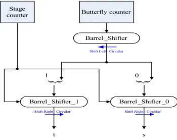
To realize equation (2.1), Cohen proposed the efficient address generator architecture as shown in Fig. 2.2. The main idea is appending 0 and 1 to MSB of the content of butterfly counter then using barrel shifters to realize the rotation.
Butterfly counter Stage counter Barrel_Shifter_0 Barrel _Shifter_1
Shift Right Circular
}
}
01
t
Shift Right Circular
s
Fig. 2.2 Data address generator for radix-2 FFT in Cohen’s scheme
We can modify Cohen’s DIB-ordered addressing scheme to direct ordered addressing scheme to suit with variable-length FFT design. The data address pair <s, t> can be described as the following equation (2.2) composed of the contents of the butterfly counter and the stage counter. supported length FFT longest the : N content counter stage the : k content counter butterfly wise -bit : ] i i i i [ } , ,..., , , 1 , ,..., , { } , ,..., , , 0 , ,..., , { 2 0 1 2 3 ) ( log 2 ) ( log 0 1 3 2 1 3 ) log( 2 ) log( 0 1 3 2 1 3 ) log( 2 ) log( 2 2 − − − − − − − − − − − − = = = N N k k k N N k k k N N i i i i i i i i i t i i i i i i i s (2.2)
Chang [6] proposed a variable-length data address generator, which was modified from Cohen’s fixed-length data address generator. Chang’s design includes an extra barrel shifter that rotates the content of butterfly counter circular left before bit appending operations and then rotates circular right followed by bit appending operations. This design not only alternates Cohen’s scheme to direct butterfly operation order, but also adapts to varying FFT lengths. The block diagram is shown in Fig. 2.3.
Butterfly counter Stage
counter
Barrel _Shifter _0 Barrel_Shifter_1
Shift Right Circular
}
}
01
t
Shift Right Circular
s Barrel _Shifter
Shift Left Circular
In order to achieve high-performance variable-length FFT operations and data accesses, we propose the following data address generator. The design covers seven different FFT lengths including 64, 256, 512, 1024, 2048, 4096, and 8192 points, which cover all the required FFT lengths by 802.11a, 802.16a, DAB, DVB-T, VDSL and ADSL. Furthermore, the proposed data address generator significantly improves the address generator mentioned above, by considering radix-22 DIF FFT algorithm and variable-length FFT operations, and by simplifying the original area-consuming barrel-shifter based designs with simpler multiplexer-based addressing functions.
The four addresses required by radix-22 butterfly PE correspond to the 4 different banks. The addresses are denoted as <s, t, u, v> which can be calculated by the equation (2.3), where N is the longest FFT length supported, k is the stage counter content, and
2 0 1 2 3 ) ( log 2 ) ( log j ... j j j ] j [ 2 − 2 − = N N
i is butterfly counter content.
2 0 1 2 log 1 log log 2 log 1 log 2 0 1 2 log 1 log log 2 log 1 log 2 0 1 2 log 1 log log 2 log 1 log 2 0 1 2 log 1 log log 2 log 1 log ] ... 11 ... [ ] ... 10 ... [ ] ... 01 ... [ ] ... 00 ... [ j j j j j j j v j j j j j j j u j j j j j j j t j j j j j j j s K N K N K N N N K N K N K N N N K N K N K N N N K N K N K N N N − − − − − − − − − − − − − − − − − − − − − − − − − − − − = = = = (2.3) Butterfly counter [10:0] SIB MUX array 01 SIB MUX array 00 SIB MUX array 10 SIB MUX array 11 + Comparator Ca rry -in cont ro lle r Stage Counter 1 2 4 8 16 32 128 13 12 11 10 9 8 6 Reset Signal MU X MUX Mode select s [12:0] t [12:0] u [12:0] v [12:0]
Fig. 2.4 Block diagram of the proposed variable-length data address generator
The hardware block diagram of variable-length data address generator is shown in Fig. 2.4. In the figure, “carry-in controller” adds the carry-out signal from butterfly counter to the LSB or its left immediate bit of the stage counter to alternate the counter step of the stage counter between one and two; “comparator” compares stage counter content with the maximum stage
count corresponding to each FFT length and reset all counters if they are equal; input signal “mode select” controls the butterfly counter step and maximum stage count to vary FFT length; “SIB MUX array” denotes shift-insertion-bypass multiplexer array. It greatly simplifies the address generator of Fig. 2.5 and Fig. 2.6, as will be detailed below.
Insert symbol 0
Insert
symbol 1 Bypass Shift 1
MUX_n
MUX_con_nFig. 2.5 Block diagram of MUX_n module
MUX_0 MUX_1 MUX_2 MUX_3 MUX_9 MUX_10 MUX_11 MUX_12 Butterfly counter [10:0] Data address [12:0] Symbol [1:0] x x x x MUX_con_12 MUX_con_11 MUX_con_10 MUX_con_9 MUX_con_3 MUX_con_2 MUX_con_1 MUX_con_0
Fig. 2.6 The architecture of Shift-insert-bypass MUX array
In our design, we define several functions to simplify the design to replace those area-consuming barrel shifters with much simpler multiplexers. The functions include the required left shift operations, symbol bit insertion operations, and bypass the remaining bits, for the realization of the variable-length data address generation algorithm. Detailed architecture of the shift-bypass-insertion multiplexer array is shown in Fig. 2.6. In the figure, the input signal “symbol” to MUX_n module can be 00, 01, 10, or 11, where block diagram of MUX_n is shown in Fig. 2.5, and function of MUX_n out-put is explained in Table 2.3. Timing and area
comparisons of data address generator between SIB-MUX array approach and barrel shifter approach are shown in Table 2.4, and the result is synthesized by TSMC 0.25µm standard cell library with Synopsis Design Analyzer.
Table 2.3 Output functions of the MUX_n.
Output Function Insert symbol 0 (I0) Select symbol bit 0 as the n-th bit of data address.
Insert symbol 1 (I1) Select symbol bit 1 as the n-th bit of data address. Bypass (BP) Select the n-th bit of butterfly counter as the n-th bit of data address.
Shift 2 (S2) Select the (n-2)-th bit of butterfly counter as the n-th bit of data address.
Table 2.4 Comparison of DAG units.
SIB-MUX array Barrel shifter (Fig.2.3)
No. of cells 143 229
Total gate counts 169 352
Path delay 5.72ns 7.14ns
2.1.2 Variable-length Coefficient Address Generator
The basic coefficient address generating function is mainly a counter with an adjustable counting step to realize varying stages and allow for varying FFT lengths. Hence, we can realize the coefficient address generator based on the content of the butterfly counter.
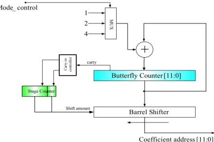
In fig. 2.7, we give an example of coefficient address generator which sustains 8192, 4096, and 1024-point FFT. Butterfly Counter [11:0] Barrel Shifter carry
+
Mode_ control MU X 1 2 4 Shift amount Coefficient address [11:0] Ca rr y-in co nt ro ll er Stage Counter2.1.3 Variable-length Processing Element
Although our design is based on radix-22 DIF FFT algorithm, we can still compute a general power-of-2 FFT by adding some minor modification to the radix-22 datapath. The unified radix-22/2 datapath is shown in Fig. 2.8 and Fig. 2.9. In the fig. 2.8, the control line “select=0” programs the PE to as radix-22 mode so as to execute radix-22 algorithm, otherwise, in fig. 2.9, the four adders on the right hand side and the multiplier WN2n is bypassed so that the PE is
configured as radix-2 mode such that two radix-2 butterflies are processed simultaneously. The “swap r/i” unit, that interchanges real part with imaginary part, is to implement the required multiplication with “-j”. This shared hardware design does not increase the complexity of data address generator. + -+ -+ -+ -X X Swap r/i MU X MU X MU X MU X n N W2 n N W n N W3 0 1 0 1 0 1 0 1 Radix-22/2 select X MUX 0 1 4 N n N W+ Data in 0 Data in 1 Data in 2 Data in 3 Data out 0 Data out 1 Data out 2 Data out 3
Fig. 2.8 The radix-22 mode datapath of the PE
+ -+ -+ -+ -X X Swap r/i MU X MU X MU X MU X n N W2 n N W n N W3 0 1 0 1 0 1 0 1 Radix-22/2 select X MUX 0 1 4 N n N W+ Data in 0 Data in 1 Data in 2 Data in 3 Data out 0 Data out 1 Data out 2 Data out 3
2.1.4 Variable-length Commutate Mode
The memory access bandwidth is the critical issue in memory-based FFT processor design. An N-point memory-based FFT processor based on radix-r algorithm needs N
r N
r
log PE
operations to transform one N-point symbol. Further, each PE operation needs 2r memory accesses to read data from memory and write back to it, so that each N-point symbol requires
N Nlogr
2 memory accesses. In order to handle this requirement, there are two solutions: 1. Use a higher-radix algorithm to reduce total memory accesses.
2. Increase memory access bandwidth by distributing memory accesses into several memory banks or multiple memory ports.
However, it is expense to increase the arithmetic complexity. Further, the number of memory ports is not controlled by architecture designer but cell library provider and device vendor, and the desirable case of the in-place design is simultaneously delivering r complex data from memory to radix-r butterfly PE and writing back r complex data from output ports of butterfly PE to the data memory. Therefore, the solution of memory access bandwidth is to partition memory into r banks, and than assign r input data for radix-r butterfly PE to proper memory banks for conflict-free memory access.
There are several efforts on memory partition and addressing methods to achieve conflict-free memory access [2], [3]. The general conflict-free memory partition scheme [2] that translates sequential data count into bank index and data index of each bank is shown in equation (2.4).
r n n n t t r n n r d d d d index Data r d index Bank d d d d d count Data N n ] ... [ _ mod ) ( _ ] ... [ _ log 1 2 2 1 1 0 0 1 2 2 1 − − − = − − = = = =∑
(2.4)Similar result can also be found in Lo’s scheme derived by vertex coloring rule [3]. For
radix-r butterfly PE, this allocation algorithm can access r data from r different banks simultaneously at proper addresses according to the original data addresses. The original data address data_count can be generated according to the content of the butterfly counter and the stage counter of FFT processing. The data_index is the new address assigned to each memory bank.
The bank index generator of our design is shown in Fig. 2.10. The commutate modes of the commutator which supports the variable-length FFT mentioned above are shown in Table 2.5.
S u m _ M o d 4 S u m _ M o d 4 S u m _ M o d 4 S u m _ M o d 4 S u m _ M o d 4 S u m _ M o d 4 A 0 A 1 A 2 A 3 A 4 A 5 A 6 A 7 A 8 A 9 A 1 0 A 11 A 1 2 0 M 1 M 0
Fig. 2.10 Block diagram of bank index generator
Table 2.5 Four different commutator configuration linking desired data access port index to bank index of data.
M
1
M
0
Commutator mode
(power-of-4 point FFT)Commutator mode
(The first stage of non-power-of-4 point)
0 0
Desired write data order Desired read data order Data order in memory banks D C B A A B C D A B C D Desired write data order Desired read data order Data order in memory banks D B C A A B C D A B C D0 1
Desired write data order Desired read data order Data order in memory banks C B A D A B C D A B C D Desired write data order Desired read data order Data order in memory banks B C A D A B C D A B C D1 0
Desired write data order Desired read data order Data order in memory banks B A D C A B C D A B C D Desired write data order Desired read data order Data order in memory banks C A D B A B C D A B C D1 1
Desired write data order Desired read data order Data order in memory banks A D C B A B C D A B C D Desired write data order Desired read data order Data order in memory banks A D B C A B C D A B C D2.1.5 The Proposed Variable-length FFT Processor Architecture
Bank_3
Bank_2
Bank_1
Bank_0
Co m m ut ator _r ea d C om m uta tor _w rit eRadix-2
2/2 BF
Reg Variable-Length Coefficient Address GeneratorCoefficient generator
Variable-Length Data Address Generator
Controller coefficients Reg Reg Reg R22/R2 select Reg Reg Reg Reg
Fig. 2.11 Block diagram of the proposed FFT processor
A general memory-based FFT processor structure mainly consists of a PE, a main memory, ROM for twiddle factor storage, and a controller. The main memory stores processed data. The controller contains three functional units: data memory address generator, coefficient index generator, and operation state controller. The Butterfly PE is responsible for the butterfly
operations required by FFT operations.
Inside the FFT processor, operation can be divided into three major parts: memory read, data processing, and memory write back. These three parts are isolated by two sets of register so that they can operate simultaneously and independently without conflict. The FFT operation diagram of our design example is shown in Fig. 2.12.
PE RE G RE G MEM READ MEM WRITE PE REG REG MEM READ MEM WRITE PE REG REG MEM READ MEM WRITE
Fig. 2.12 Pipelined data path and shared devices of FFT processor
2.2 CORDIC-based Processing Element of FFT Processor
2.2.1 The CORDIC Algorithm and ArchitectureIn many FFT applications, the butterfly processing element (PE) often is realized with complex multipliers which have characteristics of high complexity and huge amount of area. Further, for the requirement of the twiddle factor multiplications, the twiddle factors must be stored in a look-up table which is generally implemented by ROM in advance. However, since long-length FFTs are commonly used in modern applications such as 8192-point FFT in DVB-T, the look-up table approach becomes inefficient because of enormous chip area cost. For example, even if we employ the symmetric property of the sinusoid function, the total ROM space requirement is 2*12*8192 /8 = 24576(bits) ≈ 3(KB) in an 8192-point FFT with 12-bit accuracy. For this reason, the CORDIC (Coordinate Rotation Digital Computer) algorithm is proposed here to substitute for conventional complex multiplier and look-up table approach.
The CORDIC algorithm developed by Volder [7] in 1959 is a generalized algorithm that can perform vectoring and rotation operations of a two dimensional vector. The rotation operation is to compute the target vector of the initial vector and the given rotation angle θ, while the intention of the vectoring operation is to compute the angle between the start vector and the end vector. Furthermore, there are three different kinds of coordinate systems: the linear coordinate system, the circular coordinate system, and the hyperbolic coordinate system. Walther [8] extend the algorithm to compute multiplication, division, and hyperbolic functions. The applications of CORDIC-based are 3-D graphic [9], [10], adaptive filter [11], floating point unit, DSP processor, and so on.
When employing CORDIC algorithm to FFT PE, we only investigate the most popular circular coordinate system and the rotation mode operations. The basic theory of the CORDIC algorithm is reviewed as follows section.
The rotation operations are approached by a sequence of micro-rotations (elementary angles) using only shift-and-add operations, and therefore it is very suited for VLSI implementation and DSP applications. There have been numerous improved CORDIC algorithms and structures proposed ever since its introduction. Most of the CORDIC algorithms assume a constant scale factor for the ease of scale factor compensation. However, they have to rotate even when the residual rotation angles have converged [12], [13], [14], [15]. In some cases, they either have to do accurate but slow decision operations for rotation directions or do rough direction decisions at the expense of extra compensation operations [12], [13]. To speedup CORDIC operations, the following techniques are widely used: (1) use carry-free redundant addition scheme [12], [13], [16-19]; (2) fast decision of rotation directions with only a few most significant digits (MSDs) of the control parameters [12], [13], [16-19]; (3) skip unnecessary rotations; (4) effectively recode rotation angles for saving rotation iterations [20]; (5) apply radix-4 rotation schemes [17], [21], [22], [23], to reduce iteration numbers; and (6) predict the rotation sequence for parallel and pipelined processing.
Some of the mentioned techniques result in variable scale factors. Variable scale factors have the trouble of complicated scale factor computation followed by penalty compensation [18], [19]. Due to the considerable overhead generated by variable scale factor, most of the existing radix-4 CORDIC algorithms resort to constant scale factor approach [17], [22]. However, these constant-scale-factor CORDICs are basically hybrid radix-2 and radix-4 algorithms. As a result, their iteration numbers are not fully reduced. Recently, we proposed CORDIC algorithms with variable scale factors [21] skip unnecessary rotations and at the same time perform low-complexity on-line decompositions and compensations for the variable scale factors. Specifically, the radix-4 algorithm costs less iteration (including rotations and compensations) than the existing radix-4 algorithms. The radix-4 CORDIC algorithm proposed in [23] is similar to the one in [21], except the ways they handle variable scale factors. Both designs share the same low iteration number of 0.8n. Although the very high-radix CORDIC algorithm has an extremely small iteration number, it is irregular in realization which needs multiplication-and-accumulation circuits. Its efficiency is high dependent on practical circuit optimization.
To reduce the shift-and-add operations of both rotation iterations and scale factor compensations, we will present a new table lookup recoding scheme for rotation angles and variable scale factors. The new method can speedup both the convergence rates of the residual rotation angles and our fast variable scale factor decomposition and compensation algorithm [21]. For more reduction of iteration number, the new CORDIC algorithm also applies the leading-one bit detection operations to both residual rotation angles and decomposition of variable scale factors.
2.2.2 The New Angle Decomposition Scheme
For speeding up convergence, first we detect the leading-one (leading-zero) bit positions,
for positive (negative) residual angle zi, respectively, in the i-th iteration. This action can avoid
unnecessary rotations required by conventional CORDIC algorithms. Then the most significant r
bits (denoted as zi,r ), counted from the leading-one (or leading-zero) bit of zi, are used to access
δm and δn information from a table. These two retrieved parameters correspond to a combined
rotation angle tan-12-m + tan-12-n that best matches zi,r (in a least-square error sense), which makes
zi,r – ( tan-12-m + tan-12-n ) as close to zero as possible. This approach corresponds to the following
iteration operation (2.5), and this iteration results in a variable scale factor described as the following equation (2.6). + + − = + − − = + = − = ⇒ + = − = − − + − + − − + − + + − + + + − + + − + − + ) 2 2 ( ) 2 1 ( ) 2 2 ( ) 2 1 ( ' 2 ' ' 2 ' 2 ' 2 ' ) ( 1 ) ( 1 1 1 1 1 1 1 1 1 i i i i i i i i i i i i n m i n m i i n m i n m i i i n i i i n i i i m i i i m i i x y y y x x x y y y x x x y y y x x (2.5)
∏
∏
= − − = + + = = I i m n I i n m i i i i K 1 2 2 1 1 2 1 2 1 1 cos cosθ
θ
(2.6)In generalization, we may include more than two δn’s to speedup the convergence rate.
However, the computational complexity increases significantly, and therefore we only investigate the case of two combined direction parameters here. Similar techniques can be extended to the general case. Based on equation (2-5), some lookup tables for the residual rotation angles can be constructed by computer search with the closest match as mentioned before. In a sense, it
approximately amounts to a radix-2r CORDIC algorithm, by examining the MSB part zi,r of the
residual rotation angle zi,. Since an optimal table depends on the iteration index i, it is better to
have an optimized lookup table for each i. However, it will increase the table size accordingly.
From easy Taylor expansion, we can get tan-12-i ≈ 2-i when i>>0. Then, in computer simulations,
we find that it is enough to have good results by using only two different tables, as shown below.
Here, we take r= 4 bits (i.e., radix-24) as a design example. Table 2.6 shows the stored
optimized m and n of the δm and δn patterns, corresponding to the zi,r information. From Taylor’s
expansion of θk = tan-12-k , we find that the binary patterns of θ0 and θ1 are noticeably different
from those of the θk’s, k>1. Therefore, two different tables are used for the cases of k= {0,1} and
k>1, respectively, where k is the leading-one (or leading-zero) bit position of the residual rotation
Table 2.6 Recoding table for the decomposition of residual rotation angle Optimized patterns of m and n
k=0,1 k>1 θi(2-k~2-k-3) m n m n 1000 k k+3 k k+4 1001 k k+2 k k+3 1010 k k+2 k k+2 1011 k k+1 k k+1 1100 k k+1 k k+1 1101 Unused , for θ0=0 ~ π/4 k k+1 1110 Unused , for θ0=0 ~ π/4 k-1 k+5 1111 Unused , for θ0=0 ~ π/4 k-1 k+3
2.2.3 Table reducing scheme
In above description of new angle encoding scheme, the given table size does not include
the term n*p for {tan-12-i, i=0,1,2,…,n-1}, required by conventional CORDIC algorithms. We
can find the equation (2.7) in Taylor expansion.
range error max the is ) ( where ), ( ) 1 ( tan 7 7 2 2 3 1 x O x O x x x x + + − = − (2.7)
Table 2.7 the table of tan-12-i value for the 12-bit accuracy
i tan-12-i ( radius ) tan-12-i ( degree )
1 0.463867 ( 0011101101102 ) 26.565051 ( 1101010010002 ) 2 0.245117 ( 0001111101102 ) 14.036243 ( 1110000010012 ) 3 0.124512 ( 0000111111112 ) 7.125016 ( 1110010000002 ) 4 0.062500 ( 0000100000002 ) 3.576334 ( 1110010011102 ) 5 0.031250 ( 0000010000002 ) 1.789911 ( 0111001010002 ) 6 0.015625 ( 0000001000002 ) 0.895174 ( 0011100101002 ) 7 0.007813 ( 0000000100002 ) 0.447614 ( 0001110010102 ) 8 0.003906 ( 0000000010002 ) 0.223811 ( 0000111001012 ) 9 0.001953 ( 0000000001002 ) 0.111906 ( 0000011100102 ) 10 0.000977 ( 0000000000102 ) 0.055953 ( 0000001110012 ) 11 0.000488 ( 0000000000012 ) 0.027976 ( 0000000111002 )
In equation (2.7), if we need n bit output precision and x = 2-i, we can ignore the second
item when i ≥ n/3. Then, we can get the tan-12-i value by shifting tan-12-(i-1). By the method, we
only need n/3 words to store the angle tan-12-i, replacing the traditional n words. For instance, the
terms of tan-12-i value which have be stored in ROM are 4 and 5 for radius and degree
representation respectively.
2.2.4 On-line variable factor compensation
For low-complexity on-line variable scale factor compensation described by equation (2.6), here we further improve and speedup our previous efficient variable scale factor algorithm, by using a on-line variable factor compensation. The whole improved algorithm is detailed below.
Rewriting equation (2.6), K can be first transformed to i i n m i K 2 2 1 2 1 2 1 1 − − + + = (2.8)
The same in Taylor, we can find Ki = (1-2-(2m+1))(1-2-(2n+1))+O(2-(4m+1)). From this expansion,
the Ki will approximate to 1 when i > (n/2)-1. Therefore, we can get the most suitable scale
factor compensation values when we get the rotation items δm and δn. And the compensation
computation can also be calculated by shift-and-add operation. In every time scale factor
compensation, we will have an error item O(2-(4m+1)), when i < (n/4)-1. The error will be store
and than be compensated just after the rotation operations i > (n/2)-1.
2.2.5 The Overall Operation Flow
In summary, by combing the leading-one bit detection scheme, the residual recoding technique, and the on-line variable scale factor compensation, we have a CORDIC algorithm as detailed by the following steps:
(1) Set the initial iteration number i = 0, initial residual angle z0 = θ, initial rotation vector
(x0, y0) = (x, y), and initial exponent residual T0 = 0. If θ = 0, then (x’, y’) = (x, y), and
exit the rotation iteration. Otherwise, proceed to step (2).
(2) Check leading-one bit position k and obtain zi,r of zi,. If zi≠0, go to step (3). Otherwise, zi
= 0: rotation operations are completed and set the total iteration number I=i-1; go to step (5).
(3) Using zi,r retrieve the optimized m and n of δm and δn, and then get the value of tan-12-m
and tan-12-n from lookup tables. To perform the iteration as shown in equation (2.5) and
zi+1 = zi– ( tan-12-m + tan-12-n ). And the scale variable compensation:
)
2
1
(
)
2
1
(
),
1
4
/
(
If
(2 1) 1 ' 1 ) 1 2 ( 1 ' 1 + − + + + − + +−
=
−
=
−
<
i i l i i l i iy
y
x
x
n
i
) 2 1 ( ) 2 1 ( ), 1 4 / ( If (2 1) 1 ' 1 ) 1 2 ( 1 ' 1 + − + + + − + + + = + = − > i i l i i i l i i i e y y e x x n i
(4) Set i=i+1, go to step (2).
(5) Calculation complete and the output values are (xi+1, yi+1).
Fig. 2.13 shows the architecture for our new CORDIC processor. However, for the consideration of high-speed operations, they can be put in a pipelined structure in cascade. The pipelined structure is particularly efficient for the applications that require intensive and sustaining vector rotation operations.
x(i+1)
±
Barrel Shifter -y(i+1) Barrel Shifter -ROM (tan-1 2-i ) Detect leading-one Circuit ROM (Angle encode table) m(i+1) n(i+1) θ(i+2) Scale factor erroraccumulator T(i) T(i+1)
+
±
x(i) m(i) n(i) Residue Angle θ(i+1) ROM ) 2 1 ( ln -)) 2 ln(cos(tan−1 −i − −(2i+1)+
Barrel Shifter±
Barrel Shifter±
Barrel Shifter±
Barrel Shifter y(i)Fig. 2.13 The structure of new CORDIC algorithm
2.2.6 Simulations Results
Based on the structures shown in Fig. 2.13, we performed fixed-point hardware simulations using Matlab & Verilog hardware description language, assuming 8-bit, 12-bit and 16-bit accuracy (including 2-bit integer part). Exhausted simulations were conducted for all the rotation angles in the range of 0˚~ 45˚. The simulation result will be shown in the table 2.8.
Table 2.8 Simulation results in different output bits precision with our new CORDIC algorithm
Output precision 8 12 16
Angle composition 1.835 2.727 3.644
Scale factor composition 1.786 3.092 4.153
Average
Overall iteration 2.437 3.482 4.424
Angle composition 3 4 5
Scale factor composition 4 5 6
Worst case
Overall iteration 4 5 6
3. Conclusion
In section 2.1, we propose an in-place memory-based variable-length FFT processor architecture, which is suited for multi-mode and multi-standard OFDM systems including 802.11a, 802.16a, DAB, DVB-T, and VDSL. The design is featured with the following low-complexity components including: a butterfly PE, a variable-length data address generator, and a variable-length coefficient address generator. The design is published in ISCAS’04 and currently under final EDA realization. The design will be taped out soon in a few weeks. Due to page limitation, we just include our results on channel estimation in the appendix. The result is a high-performance DCT-based channel estimation algorithms which is accepted by ICC04.
In addition, the new CORDIC algorithm considerably reduces the iteration number efficiently. It is achieved by combining several design techniques, including efficient high radix rotation scheme, angle encoding, leading-one bit detection, and on-line variable factor compensation. Our further work is to implement this new CORDIC-based PE for FFT processors of OFDM systems.
4. References
[1] D. Cohen, “Simplified Control of FFT Hardware,” IEEE Trans. Acoust., Speech Signal Processing, Vol. ASSP-24, pp. 577-579, Dec. 1976.
[2] L. G. Johnson, “Conflict Free Memory Addressing for Dedicated FFT Hardware,” IEEE Transactions on Circuit and System-II: Analog and Digital Signal Processing, Vol. 39 No.5, pp.312-316, May 1992.
[3] H. F. Lo, Ming-Der Shieh, and Chien-Ming Wu, “Design of an Efficient FFT Processor for DAB System,” IEEE International Symposium on Circuits and Systems, Vol. 4, pp. 654 –657, 2001.
[4] Y. Ma, “An Effective Memory Addressing Scheme for FFT Processors,” IEEE Transactions on Signal Processing, Vol. 47 Issue: 3, pp. 907-911, March 1999.
[5] Y. Ma and L. Wanhammar, “A Hardware Efficient Control of Memory Addressing for High-Performance FFT Processors,” IEEE Transactions on Signal Processing, Vol. 48 Issue: 3, pp. 917-921, March 2000.
[6] C. K. Chang, Investigation and Design of FFT core for OFDM Communication Systems, NCTU, Master Thesis, June 2002.
[7] J.E. Volder, “The CORDIC Trigonometric Computing Technique,” IRE Trans. Electronic Comput., Vol. EC-8, 1959, pp. 330-334.
[8] J.S. Walther, “A unified algorithm for elementary functions,” Proceedings of the Spring joint computer conference, 1971, pp.379-385
[9] H.M. Amhed, “Signal processing algorithms and architectures,” PhD Disscrtation, Stanford University, 1982.
[10] Y.H. Hu, “CORDIC-based VLSI architectures for digital signal processing,” IEEE Signal Process. Mag., 1992, (7), pp.16-35.
[11] K. Parhi and E.F. Deprettere, “Annihilation-reordering look-ahead pipelined CORDIC-based RLS adaptive filters and their application to adaptive beamforming,” IEEE Trans. Signal Process., 2000, 48, (8), pp. 2414-2430.
[12] N. Takagi, T. Asada, and S. Yajima, “Redundant CORDIC Methods with a Scale Factor for Sine and Cosine Computation,” IEEE Trans. On Computers, Vol. 40, No. 9, September 1991, pp. 989-995.
[13] J. Duprat and J.M. Muller, “The CORDIC Algorithm: New Results for Fast VLSI Implementation,” IEEE Trans. on Comput., Vol. 42, No. 2, February. 1993, pp. 168-178. [14] M. Kuhlmann and K.K. Parhi, “A High-Speed CORDIC Algorithm and Architecture for
DSP Applications,” SiPS 99. 1999 IEEE Workshop, 1999, pp. 732 –741.
[15] D.S. Phatak, “Double Step Branching CORDIC: A New Algorithm for Fast Sine and Cosine Generation,” IEEE Trans. on Computer, Vol. 47, No. 5, May 1998, pp. 587-602. [16] J.R. Cavallaro and N.D. Hemkumar, “Redundant and On-line CORDIC for Unitary
Transformations,” IEEE Trans. Comput., Vol. 43, No. 8, August 1994, pp. 941-954.
Rotation,” IEEE Trans. Comput., Vol. 41, No. 8, August 1992, pp. 1016-1025.
[18] M.D. Ercegovac and T. Lang, “Redundant and on-line CORDIC: Application to Matrix Triangularization and SVD,” IEEE Trans. Comput., Vol. 39, No. 6, June 1990, pp. 725-740. [19] H.X. Lin and H.J. Sips, “ON-line CORDIC Algorithms,” IEEE Trans. Comput., Vol. 39,
No. 8, August 1990, pp. 1038-1052.
[20] Y.H. Hu, and S. Naganathan, “An Angle Recoding Method for CORDIC Algorithm Implementation,” IEEE Trans. on Computers, Vol. 42, No. 1, January 1993, pp. 99-102. [21] C.C. Li and S.G. Chen, “A Radix-4 Redundant CORDIC Algorithm with Fast On-Line
Variable Scale Factor Compensation,” Proc. of 1997 IEEE International Conference on Acoustic, Speech and Signal Processing, Munich, Germany, pp. 639-642.
[22] M.R.D. Rodrigues “Hardware Evaluation of Mathematical Functions,” IEE Proc., Vol. 128, Pt. E, No. 4, July 1981.
[23] E. Antelo, J. Villalba, D. Bruguera, and E.L. Zapata, “High Performance Rotation Architectures Based on the Radix-4 CORDIC Algorithm,” IEEE Trans. on Computers, Vol. 46, No. 8, August 1997, pp. 855-870.
APPENDIX 1: Paper accepted by ISCAS2004, May, 2004, Vancouver, Canada. DESIGN OF AN EFFICIENT VARIABLE-LENGTH FFT PROCESSOR
Chung-Ping Hung, Sau-Gee Chen and Kun-Lung Chen Department of Electronics Engineering & Institute of Electronics
National Chiao-Tung University 1001 Ta Hsueh Rd, Hsinchu, Taiwan, ROC
ABSTRACT
In this paper, we propose an efficient variable-length FFT processor architecture suitable for multi-mode and multi-standard OFDM communication systems. The FFT processor is based on radix-22 DIF FFT algorithm and also supports non-power-of-4 FFT computation. The design contains an efficient processing element (PE), which can execute radix-22 butterfly (BF) operations, as well as radix-2 BF operations. Moreover, in order to achieve high-performance variable-length FFT operations and data accesses, an efficient variable-length address generator and twiddle factor generator are designed. The design has the merits of low complexity and high speed performance. The designs consider seven different FFT lengths including 64, 256, 512, 1024, 2048, 4096, and 8192 points, which cover all the required FFT lengths by 802.11a, 802.16a, DAB, DVB-T, VDSL and ADSL.
1. INTRODUCTION
Fast Fourier Transform (FFT) unit, is one of the critical components in OFDM (orthogonal frequency division multiplexing) systems. Because of high real-time throughput rate demand by current OFDM systems, such as ADSL, VDSL, 802.11a, 802.16, DAB, and DVB-T, an efficient FFT processor is required for real-time operations.
FFT architectures can be categorized as two types: the pipelined architectures and the memory-based architectures [1], [2], [3]. For hardware simplicity, this work only focuses on memory-based designs. Memory-based architectures generally include a single butterfly PE (or more than one to enhance computation power), a centralized memory block to store input or intermediate data, and a control unit to handle memory accesses and data flow direction.
Since the existing OFDM communication systems all have similar baseband architectures and FFT/IFFT operations, it is advantageous to design a single variable-length memory-based FFT/IFFT module suitable for multi-mode and multi-standard operations. With this consideration, there are many design problems to be addressed and overcome for the realization of an efficient
variable-length FFT/IFFT processor. Some of the key design issues include: (1) a high-performance PE capable of executing FFT butterfly operations for various FFT algorithms; (2) a high-performance data-address generator that supports in-place variable FFT length data accesses; (3) an efficient multi-bank memory structure that support low cycle-count conflict-free data accesses; (4) an efficient address generator for variable-length twiddle factor accesses or generations .
There are some PE designs in the literature [1], [4], [5]. Here we adopt the conventional multiplier-and-adder based butterfly structure, based on radix-4 FFT algorithm, and also consider general power-of-two FFT operations. For the complex multiplication, four real multipliers are replaced by three multipliers. For the design of variable-length address generator, not much was proposed in the past. However, there are some efficient conflict-free in-place memory addressing schemes [2], [3], [5], [6].All these designs require area-consuming barrel shifters. We will propose a much efficient design which has a small area, meanwhile supports variable-length FFT data addressing. Correspondingly, we will also need a four-bank memory that matches the in-place memory address generator for high-bandwidth data access.
For twiddle factor addressing and generation, we propose an on-line generation design, which has a much smaller area and higher speed than conventional ROM-based designs. The design is detailed in [7].
2. MEMORY-BASED FFT ARCHITECTURES
A general memory-based FFT processor structure mainly consists of a PE, a main memory, ROM for twiddle factor storage, and a controller. The main memory stores processed data. The controller contains three functional units: data memory address generator, coefficient index generator, and operation state controller. The Butterfly PE is responsible for the butterfly operations required by FFT operations.
For performance consideration, ideally the PE should simultaneously fetch r complex data from memory then write back r complex computed output data to the data
barrel shifter 0 butterfly counter stage counter barrel shifter r-1 address switching Data_index_0 Data_index_r-1 Fig. 1 Block diagram of an in-place, conflict –free,
multi-bank data address generator
Bank_3 Bank_2 Bank_1 Bank_0 C om m utat or _rea d C om m ut at or _w rite Radix-22/2 BF Re g Re g Re g Re g Re g Re g Re g Re g MU X MU X MU X MU X VL_CAG Coefficient ROM VL_DAG Counter R22/R2 select coefficients
Fig. 2 Block diagram of the proposed variable-length FFT processor
memory. Therefore, memory design should consider multi-bank data addressing and partition the memory into r banks for r concurrent conflict-free data accesses. There are some efforts on memory partition and addressing methods to achieve conflict-free memory access [5], [6]. In summary, those approaches can be described by the following efficient functions [5]:
r n n n t t r n n r d d d d index Data r d index Bank d d d d d count Data N n ] ... [ _ mod ) ( _ ] ... [ _ log 1 2 2 1 1 0 0 1 2 2 1 − − − = − − = = = = ∑ (1)
Those mapping functions are efficient in that they are regular and simple for varying butterfly operations and conflict-free memory accesses. They can be realized by the data address generator structure shown in Fig. 1 [5]. In the figure, data_index_n is the new address in the assigned memory bank. The butterfly counter value indicates the sequence number of a butterfly operation from 0 to N/r. This counter value is appended a symbol value to its LSB, ranging from 0 to r-1, and shifted left by an amount equal to the content of the stage counter.
These r input data addresses for butterfly PE are translated to r corresponding bank indices and addresses
+ + + + + + + + X X X Swap r/i MU X MU X MU X MU X n N W2 n N W n N W3 0 1 0 1 0 1 0 1 select DataIn_0 DataIn_1 DataIn_2 DataIn_3 DataO DataO DataO DataO
Fig. 3 Data path of radix-22/2 processing element within the memory banks. This facilitates r simultaneous conflict-free read operations from the r memory banks. Although this address generator is very efficient, it is area consuming, and it is only suitable for fixed-length FFT operations. Later, we will propose a variable-length address generator with smaller area than the design of Fig. 1.
3. THE PROPOSED VARIABLE-LENGTH FFT ARCHITECTURES
Our design is an 8192-point variable-length FFT processor suited for various FFT lengths of 802.11a, 802.16, DAB, DVB-T, and VDSL. Block diagram of our design is shown in Fig. 2.
3.1 The Butterfly PE
Although our design is based on radix-22 DIF FFT algorithm, we can still compute a general power-of-2 FFT by adding some minor modification to the radix-22 datapath. The unified radix-22/2 datapath is shown in Fig. 3. In the figure, the control line “select=0” programs the PE as radix-22 mode so as to execute radix-22 algorithm, otherwise, the four adders on the right hand side and the multiplier n
N
W2 is bypassed so that the PE is configured as
radix-2 mode such that two radix-2 butterflies are processed simultaneously. The “swap r/i” unit, that interchanges real part with imaginary part, is to implement the required multiplication with “-j”. This shared hardware design does not increase the complexity of data address generator.
3.2 The variable-length data address generator (DAG) The proposed data address generator significantly improves the address generator mentioned in section 2, by
considering radix-22 DIF FFT algorithm and
variable-length FFT operations, and by simplifying the original area-consuming barrel-shifter based designs with a few simpler multiplexer-based addressing functions. The four addresses required by radix-22 butterfly PE in
power-of-4 point FFT correspond to the 4 different banks. The Butterfly counter [10:0] SIB MUX array 01 SIB MUX array 00 SIB MUX array 10 SIB MUX array 11 + Comparator Ca rr y -i n c o nt ro ller Stage Counter 1 2 4 8 16 32 128 13 12 11 10 9 8 6 Reset Signal MU X MU X Mode select s [12:0] t [12:0] u [12:0] v [12:0] Fig .4 Block diagram of the proposed variable-length data addresses of the generator addresses are denoted as <s, t, u, v> which can be calculated by the following equations.
4 0 1 3 log 2 log 1 log 3 log 2 log 4 0 1 3 log 2 log 1 log 3 log 2 log 4 0 1 3 log 2 log 1 log 3 log 2 log 4 0 1 3 log 2 log 1 log 3 log 2 log ] ... 3 ... [ ] ... 2 ... [ ] ... 1 ... [ ] ... 0 ... [ 4 4 4 4 4 4 4 4 4 4 4 4 4 4 4 4 4 4 4 4 i i i i i i i v i i i i i i i u i i i i i i i t i i i i i i i s k N k N k N N N k N k N k N N N k N k N k N N N k N k N k N N N − − − − − − − − − − − − − − − − − − − − − − − − − − − − − − − − = = = = (2) where i =[ilog4(N)−2ilog4(N)−3...i2i1i0]4 is the
butterfly counter content, and k is the stage counter content.
On the other hand, in non-power-of-4 point FFT operations, the radix-22 butterfly should be reconfigured as two radix-2 butterflies in the first stage of FFT operations. Hence, the data address generator should provide two different address-generation modes to accommodate both power-of-4 and non-power-of-4 point FFT operations.
In the first stage of non-power-of-4 FFT operations, data addresses <s, t, u, v> required by butterfly PE are generated by the following equations.
2 0 1 2 2 log 1 log 2 0 1 2 2 log 1 log 2 0 1 2 2 log 1 log 2 0 1 2 2 log 1 log ] ... 11 [ ] ... 10 [ ] ... 01 [ ] ... 00 [ j j j j j v j j j j j u j j j j j t j j j j j s N N N N N N N N − − − − − − − − = = = = (3) where j is bit-wise representation of butterfly counter content and N is the longest FFT length supported. The generalized data address generation equations are:
2 0 1 2 log 1 log log 2 log 1 log 2 0 1 2 log 1 log log 2 log 1 log 2 0 1 2 log 1 log log 2 log 1 log 2 0 1 2 log 1 log log 2 log 1 log ] ... 11 ... [ ] ... 10 ... [ ] ... 01 ... [ ] ... 00 ... [ j j j j j j j v j j j j j j j u j j j j j j j t j j j j j j j s K N K N K N N N K N K N K N N N K N K N K N N N K N K N K N N N − − − − − − − − − − − − − − − − − − − − − − − − − − − − = = = = (4) where K is a special stage counter content, which is increased by one each time when all the radix-2 butterfly operations within the current stage are completed, or increased by two after one stage of radix-22 butterfly operations is completed.
The hardware block diagram of variable-length data address generator for our FFT processor capable of executing8192, 4096, 2048, 1024, 512, 256, and 64-point FFTs is shown in Fig. 4. In the figure, “carry-in controller” adds the carry-out signal from butterfly counter to the LSB (the shaded area) or its left immediate bit of the stage counter to alternate the counter step of the stage counter between one and two; “comparator” compares stage counter content with the maximum stage count corresponding to each FFT length and reset all counters if they are equal; input signal “mode select” controls the butterfly counter step and maximum stage count to vary FFT length; “SIB MUX array” denotes shift-insertion-bypass multiplexer array. It greatly simplifies the address generator of Fig. 1, as will be detailed below.
In our design, we define several functions to simplify the design to replace those area-consuming barrel shifters with much simpler multiplexers. The functions include the required left shift operations, symbol bit insertion operations, and bypass the remaining bits, for the realization of the variable-length data address generation algorithm. Detailed architecture of the shift-bypass-insertion multiplexer array is shown in Fig. 5. In the figure, the input signal “symbol” to MUX_n module can be 00, 01, 10, or 11, where block diagram of MUX_n is shown in Fig. 6, and function of MUX_n output is explained in Table 1. Timing and area comparisons of data address generator between SIB-MUX array approach and barrel shifter approach are shown in Table 2, and the result is synthesized by TSMC 0.25μm standard cell library with Synopsis Design Analyzer. 3.3 The variable-length coefficient address generator
Instead of using conventional ROM-based twiddle factor generation scheme, we propose a new twiddle factor generator, which has a smaller area and a higher speed than the ROM-based design. The design is presented in [7]. We will not detail it here. However, if conventional ROM-based twiddle factor generation is adopted, we can use the following efficient twiddle factor address generator, as detailed below. The basic coefficient address generating function is mainly a counter with an
adjustable counting step to realize varying stages and allow for varying FFT lengths. Hence, we can realize the coefficient address generator based on the content of the butterfly counter. Coefficient address w for the i-th butterfly of the k-th stage in radix-2, N/2c -point DIF FFT can be generated based on the following equation:
MUX_0 MUX_1 MUX_2 MUX_3 MUX_9 MUX_10 MUX_11 MUX_12 Butterfly counter [10:0] Data address [12:0] Symbol [1:0] x x x x MUX_con_12 MUX_con_11 MUX_con_10 MUX_con_9 MUX_con_3 MUX_con_2 MUX_con_1 MUX_con_0
Fig. 5 The architecture of Shift-insert-bypass MUX array Table 1 Output functions of the MUX_n. Output Function
Insert symbol 0 (I0)
Select symbol bit 0 as the n-th bit of data address.
Insert symbol
1 (I1) Select symbol bit 1 as the n-th bit of data address. Bypass (BP) Select the n-th bit of butterfly counter as the
n-th bit of data address.
Shift 2 (S2) Select the (n-2)-th bit of butterfly counter as the n-th bit of data address.
Table 2 Comparison of DAG units.
SIB-MUX array Barrel shifter (Fig.2)
No. of cells 143 229
Total gate counts 169 352
Path delay 5.72ns 7.14ns
Insert symbol 0
Insert
symbol 1 Bypass Shift 2
MUX_n MUX_con_n
Fig. 6 Block diagram of MUX_n module ) 2 mod( ) 2 (i N w= × c+k (5) where N is the longest FFT length and w is from 0 to N/2-1 that corresponds to coefficient from WN0 to
1 2−
N N
W . As mentioned previously, the content of butterfly
counter is i*2c , where 2c is the ratio of longest FFT length
to the current processed FFT length. Hence, coefficient address w can be derived from
) 2 mod( ) 2 (B N w= × k (6) Butterfly Counter[7:0] Barrel Shifter carry + Mode_control MU X 1 2 4 Shift amount Coefficient address[7:0] Ca rr y-in c o nt ro ller Stage Counter
Fig. 7 The variable-length coefficient index generator. where B is the content of butterfly counter. In a fixed-radix design, equation (6) can be implemented by shifting the content of butterfly counter to left by an amount related to the stage counter’s content. Furthermore the stage counter unit is similar to Fig. 4. The hardware block diagram which depicts a coefficient address generator for 512, 256, and 128-point FFT is shown in Fig 7.
4. CONCLUSION
In the paper, we propose an in-place memory-based variable-length FFT processor architecture, which can suit for multi-mode and multi-standard OFDM systems including 802.11a, 802.16a, DAB, DVB-T, and VDSL. The design is featured with the following low-complexity components including: a butterfly PE, a variable-length data address generator, and a variable-length coefficient address generator. The design is currently under final EDA realization and will be reported in the final paper.
5. REFERENCES
[1] D. Cohen, “Simplified Control of FFT Hardware,” IEEE Trans. Acoust., Speech Signal Processing, Vol. ASSP-24, pp. 577-579, Dec. 1976.
[2] Y. Ma, “An Effective Memory Addressing Scheme for FFT Processors,” IEEE Trans. on Signal Processing, Vol. 47 Issue: 3, pp. 907-911, Mar. 1999.
[3] Y. Ma and L. Wanhammar, “A Hardware Efficient Control of Memory Addressing for High-Performance FFT Processors,” IEEE Trans. on Signal Processing, Vol. 48 Issue: 3, pp. 917-921 Mar. 2000.
[4] L. Jia ; Y. Gao ; H. Tenhunen; “Efficient VLSI implementation of radix-8 FFT algorithm” Communications, Computers and Signal Processing, 1999 IEEE Pacific Rim Conference on , pp. 468-471, 1999.
[5] H.F. Lo, M.D. Shieh, and C.M. Wu, “Design of an Efficient FFT Processor for DAB System,” IEEE International Symposium on Circuits and Systems, Vol. 4, pp. 654-657, 2001. [6] L. G. Johnson, “Conflict Free Memory Addressing for Dedicated FFT Hardware,” IEEE Trans. on Circuit and
System-II: Analog and Digital Signal Processing, Vol. 39 No.5,
pp.312-316, May 1992.
[7] J.C. Chih and S.G. Chen, “An Efficient FFT Twiddle Factor Generator,” Submitted to Eusipco-2004.
APPENDIX 2: Paper Accepted by Internaitonal Conference on Communications, June, 2004, Paris, France
DCT-Based Channel Estimation for OFDM Systems
Yen-Hui Yeh MediaTek Inc 5F, No.1-2, Innovation Road 1 Science-Based Industrial Park
Hsinchu, Taiwan, ROC
Sau-Gee Chen
Department of Electronics Engineering and Institute of Electronics
1001 Ta Hsueh Rd Hsinchu, Taiwan, ROC
Abstract—In this paper, based on the property of channel
frequency response and the concept of interpolation in transform domain, we propose two discrete cosine transform (DCT)-based pilot-symbol-aided channel estimators, which can mitigate the aliasing error and high-frequency distortion of the direct discrete Fourier transform (DFT)-based channel estimators when the multipath fading channels have non-sample-spaced path delays. Both proposed estimators outperform the conventional DFT-based channel estimators. Of these two DCT-based estimators, one has its performance close to MMSE estimator, while the other one has the advantage of easy implementation with a little performance degradation. Furthermore, in implementation, the DCT-based estimators have the advantages of utilizing mature fast DCT algorithms and architectures, which is favorable to matrix-based channel estimators.
Keywords-OFDM; channel estimation; FFT; DCT; interpolation
I. INTRODUCTION
Multicarrier systems have received much attention these days. It is a promising technique for high data rate transmission. Examples include wireless OFDM systems, such as IEEE 802.11a wireless LAN, IEEE 802.16a wireless MAN, DAB and DVB-T systems, and the wired DMT systems, such as ADSL and VDSL systems. They are robust to multipath inter-symbol interference (ISI). However, they still suffer from multipath frequency-selective fading. To remove the channel effect and do accurate data demodulation, one has to perform accurate channel estimation.
The optimal interpolation filtering in minimum mean square error (MMSE) sense is a well-known channel estimator [1], [2]. However, the statistical characteristics of a channel, i.e., autocorrelation matrix of channel frequency response and signal-to-noise ratio (SNR), must be obtained in advance. Usually this is impossible because of wide-varying channel conditions. An alternative is to use recursive least-square (RLS) method to track the channel [3]. Although RLS algorithm is quite effective, high computation complexity is a serious disadvantage. In [1], [2], the authors proposed a robust approach in which the actual autocorrelation matrix is replaced by a properly approximated matrix with small mismatch and performance loss. Although reasonable suboptimal solution is achievable using this algorithm, the required computation complexity is still very high. Hence it may not be practical.
Another popular estimator is DFT-based interpolator [4], [5]. The DFT-based channel estimator can theoretically achieve ideal lowpass interpolation and has the advantage of
low complexity by exploiting FFT algorithm. This works well when the interpolated signal is originally band-limited. For channel frequency response to be interpolated and estimated, this condition corresponds to time-limited channel impulse response. This is true when the multipath delays are all integer multiples of the sampling time and short enough so as not to cause aliasing error, if it is obtained from the IDFT of a limited number of pilot frequency responses.
If there exists any non-sample-spaced path delay, the equivalent discrete channel impulse response will be dispersive in time domain. As a result, the DFT-based interpolation process will be using the aliased data of the dispersive impulse response. This results in considerable performance degradation. To alleviate the problem, recently we proposed a DCT-based channel estimation algorithm [8] (termed DCT/EIDCT channel estimator), which is much effective than the conventional DFT-based channel interpolation algorithms. The algorithm can effectively reduce the aliasing error and achieve better interpolation performance than the popular DFT-based methods. In this paper, we will provide a more generalized and complete treatment on the DCT-based channel estimation. In addition to reviewing our recently proposed DCT/EIDCT-based channel estimation algorithm, we will also propose a fast DCT algorithm for its low-complexity realization, plus that we will propose another DCT-based channel estimator (termed IDCT/DCT-based channel estimator). The new DCT-based channel estimators also has a much better performance than the conventional DFT-based channel estimators, while is comparable with the DCT/EIDCT method. In addition, the new DCT-based channel estimators have the advantages of utilizing mature fast-DCT algorithms and architectures. They can be implemented with even lower complexity compared with DFT-based channel estimators.
In section 2, we will describe the OFDM system model and DFT-based channel estimators. Two new DCT-based channel estimators will be introduced in section 3, followed by their simulation results in section 4 and finally the conclusion.
II. OFDMSYSTEM MODEL AND DFT-BASED CHANNEL
ESTIMATORS
A. OFDM System Model
First, the transmitted data is split into several low-rate streams and then these data streams are transmitted in different subcarriers. We assume the data transmitted at the k-th
This work was supported by National Science Council, Taiwan, under the grant contracts NSC 92-2219-E-009 -017 and NSC 92-2220-E-009 -021