應用於WiMAX之雙增益模式互補金氧半低雜訊放大器設計
64
0
0
全文
(2) 應用於 WiMAX 之雙增益模式 互補金氧半低雜訊放大器設計 Design of Dual Gain Mode CMOS LNA for WiMAX Applications 研 究 生:梁書旗. Student. : Shu-Chi Liang. 指導教授:溫瓌岸 博士. Advisor. : Dr. Kuei-Ann Wen. 共同指導:溫文燊 博士. Co-Advisor. : Dr. Wen-Shen Wuen. 國 立 交 通 大 學 電子工程學系 電子研究所碩士班 碩 士 論 文. A Thesis Submitted to Department of Electronics Engineering & Institute of Electronics College of Electrical & Computer Engineering National Chiao Tung University in Partial Fulfillment of the Requirements for the Degree of Master in Electronic Engineering June 2007. 中 華 民 國 九 十 六 年 六 月.
(3) 應用於 WiMAX 之雙增益模式 互補金氧半低雜訊放大器設計. 學生:梁書旗. 指導教授: 溫瓌岸 博士 共同指導教授: 溫文燊 博士. 國立交通大學 電子工程學系 電子研究所碩士班. 摘要 本論文主要討論設計一應用於 WiMAX 之雙增益模式射頻低雜訊放大器。雙 增益模式之設計可提高電路的動態操作範圍。兩模式只需用同一套輸入端匹配電 路。多閘極電晶體技術加入此電路中以提高線性度。本電路以 0.13 微米 CMOS 製程製作,操作頻率範圍為 2.3 至 2.7GHz。此電路建立了行為模型,並藉此行 為模型來幫助縮短電路設計週期。. i.
(4) Design of Dual Gain Mode CMOS LNA for WiMAX Applications Student:Shu-chi Liang. Advisor : Dr. Kuei-Ann Wen Co-advisor : Dr. Wen-Shen Wuen. Department of Electronics Engineering Institute of Electronics National Chiao-Tung University. Abstract In this thesis, a dual-gain mode design of a direct-conversion CMOS RF LNA for IEEE 802.16e (WiMAX) applications is presented. Two gain modes with one switch stage are designed in the purposed LNA to enlarge the dynamic range. It needs only one common input matching network for different gain modes. Multiple Gated Transistors topology is integrated for linearity enhancement. The circuit is fabricated in 0.13μm CMOS process, and it is designed for operation frequency of 2.3 to 2.7 GHz. A behavior model of the circuit is constructed to facilitate the design cycle.. ii.
(5) 誌謝 這本論文得以完成,首先非常感謝溫瓌岸教授讓我有機會進入 TWT 實驗 室,並給予我們豐富的資源、良好的學習環境,以及論文寫作的大方向。感謝溫 文燊教授給予細心與耐心的指導,讓我在研究的路上走得平順。並感謝各位口試 委員們-詹益仁教授與陳巍仁教授提供的寶貴建議與指教。 感謝實驗室的學長姐們的指導與照顧:美芬學姐、嘉笙學長、哲生學長、文 安學長、晧名學長、立協學長、俊閔學長、志德學長、振威學長、俊憲學長、懷 仁學長及彥宏學長等。學長姐們的幫助與指導讓我獲益良多。 感謝實驗室的同學們-家岱、閎仁、建龍、漢健、昱瑞、建毓、世基,以及 曾經一起奮鬥過的義凱、翔琮、凱信、函霖,兩年來在課業和日常生活上總是相 互的扶持,一起高興、一起嬉笑、一起度過難關。還有給予我信心與勇氣的學弟 們-佳欣、磊中、國爵、柏麟、俊彥、士賢、謙若,同時也要感謝實驗室的助理 們-苑佳、淑怡、慶宏、恩齊、怡倩、智伶、宛君、嘉誠,幫忙實驗室裡大大小 小的事,讓我們能更專心於研究工作。 最後,我要感謝家人無怨無悔的付出與支持,感謝好友們給我的鼓勵,最後 感謝關心我與幫助我的人,僅以此論文與我的家人及好友分享我的收穫與喜悅。. 梁書旗 2007 年 6 月. iii.
(6) Contents 摘要.................................................................................................................................i Abstract ..........................................................................................................................ii 誌謝.............................................................................................................................. iii Contents ........................................................................................................................iv List of Figures ...............................................................................................................vi List of Tables.............................................................................................................. viii. Chapter 1. Introduction ......................................................... 1. 1.1 Motivation...................................................................................1 1.2. Receiver Specifications...............................................................2 1.2.1. Frequency Band Selection .................................................................2. 1.2.2. Receiver Specifications......................................................................4. A.. Sensitivity and maximum input .....................................................4. B.. Adjacent and non-adjacent channel rejection.................................6. 1.2.3. Receiver Architecture.........................................................................7. 1.2.4. LNA Specifications Calculation ........................................................8. 1.3 Previous Techniques of Multi Gain Mode LNA.......................10 1.3.1. Load Switching Type .......................................................................10. 1.3.2. Current Splitting Type......................................................................12. 1.3.3. Bias Control Type ............................................................................13. 1.3.4. Core Switching Type........................................................................14. 1.3.5. Summary ..........................................................................................16. 1.4 Organization..............................................................................16. Chapter 2. Dual-gain Mode LNA Design............................ 18. 2.1 Design Concepts .......................................................................18 2.1.1. Gain Issue.........................................................................................19. 2.1.2. Linearity Issue..................................................................................20. 2.1.3. Noise Issue .......................................................................................22. iv.
(7) 2.2 Dual-gain Mode Topology ........................................................23 2.2.1. Design Footprints.............................................................................23. 2.2.2. The Proposed Dual-gain Mode LNA Topology...............................26. A. Circuit structure and operation........................................................26 B. Circuit analysis in input matching issue..........................................27 C. Linearity issue .................................................................................28 D. Noise issue ......................................................................................29. 2.3. Circuit Design ...........................................................................29 2.3.1. Input Matching Stage .......................................................................30. 2.3.2. gm (MGTR) Stage ............................................................................30. 2.3.3. Switching and Output Matching Stage ............................................31. 2.4 Simulation Results ....................................................................31. Chapter 3 Implementation and Experimental Results..... 35 3.1. Layout Consideration................................................................35. 3.2 Measurement and Analysis .......................................................36 3.2.1. Measurement Setup..........................................................................36. 3.2.2. Measurement Results .......................................................................37. 3.2.3. Analysis............................................................................................41. 3.2.4. New considerations..........................................................................41. Chapter 4 Behavior Model of Proposed LNA ................... 44 4.1 Issues of Behavior Model Construction ...................................44 4.2 Simulation Results ....................................................................47. Chapter 5. Conclusions ........................................................ 51. 5.1 Summary ...................................................................................51 5.2 Future Works.............................................................................51 Bibliography ................................................................................................................52 Vita...............................................................................................................................54. v.
(8) List of Figures Figure 1.1: Bands for WiMAX Applications in 2-6GHz range..................................3 Figure 1.2: System architecture of WiMAX receiver.................................................7 Figure 1.3: Basic LNA stages.....................................................................................10 Figure 1.4: Schematic of load switching LNA [7] .....................................................11 Figure 1.5: Load switching concept in [7]..................................................................12 Figure 1.6: Schematic of current splitting LNA [8] ...................................................13 Figure 1.7: Schematic of bias controlled LNA [10] ...................................................14 Figure 1.8: Schematic of core switching LNA [11]....................................................15 Figure 2.1: A basic cascode CMOS LNA circuit .......................................................19 Figure 2.2: Schematic and gm’’ curve of multiple gated transistors technique...........21 Figure 2.3: Schematic of modified derivative superposition LNA ............................22 Figure 2.4: The source degeneration technique..........................................................23 Figure 2.5: First designed LNA..................................................................................24 Figure 2.6: The LNA circuit with core switching technique ......................................25 Figure 2.7: The proposed Dual-gain mode LNA circuit schematic............................26 Figure 2.8: Smith charts of S11 and S22 ....................................................................33 Figure 2.9: S11 and S22 curves in dB ........................................................................33 Figure 2.10: S21, S12, NF, P1dB simulation results ....................................................34 Figure 2.11: HB IIP3 simulation results.......................................................................34 Figure 3.1: Layout of DUT 1......................................................................................36 Figure 3.2: Measurement setup ..................................................................................37 Figure 3.3: S-parameter measurement and post-simulation results............................39 Figure 3.4: NF measurement and post-simulation results ..........................................40 Figure 3.5: Harmonic balance measurement results...................................................40 Figure 3.6: Layout of DUT 2......................................................................................42 Figure 3.7: Gain and Noise comparisons between DUT1 and DUT2........................43. vi.
(9) Figure 4.1: Simple model of passive components......................................................45 Figure 4.2: Input stage of LNA behavior model.........................................................45 Figure 4.3: Output stage of behavior model...............................................................46 Figure 4.4: S11 and S22 Comparisons .......................................................................47 Figure 4.5: S21, NF and P1dB Comparisons .............................................................48 Figure 4.6: WiMAX LNA co-simulation platform.....................................................49 Figure 4.7: System co-simulation results ...................................................................50. vii.
(10) List of Tables Table 1.1:. WiMAX reference bands in 2-6GHz range .............................................3. Table 1.2:. Receiver SNR assumptions of WirelessMAN-OFDM and WirelessMAN-OFDMA Interfaces ..........................................................5. Table 1.3:. Adjacent and non-adjacent channel rejection ..........................................6. Table 1.4:. The receiver block specifications.............................................................9. Table 1.5:. The advantages / disadvantages of multi gain mode techniques .............17. Table 1.6:. Gain, P1dB, current and NF comparison of multi gain mode techniques ................................................................................................17. Table 2.1:. The component size list of proposed LNA ..............................................32. Table 2.2:. DC simulation results...............................................................................32. Table 2.3:. S-parameter simulation results.................................................................32. Table 2.4:. Harmonic Balance simulation results ......................................................33. Table 3.1:. DC measurement results ..........................................................................38. Table 3.2:. S-parameter measurement results ............................................................38. Table 3.3:. Harmonic balance measurement results...................................................38. Table 3.4:. Component size comparisons of DUT1 and DUT2.................................42. Table 4.1:. The RMSE values in the passband...........................................................49. viii.
(11) Chapter 1 Introduction WiMAX (Worldwide interoperability for Microwave Access) is a standards-based technology defined in IEEE 802.16-2004 and IEEE 802.16e-2005. It offers the delivery of last mile wireless broadband access as an alternative to wired broadband like cable and DSL[1]. Large cover range, high transmission rate and wide variety of applications are the most obvious characteristics of this new technology, and these characteristics will cause a revolution in internet accessing of “moving” mobile device, “last mile” network constructing and even the communication network recovering after disaster. The convenience of WiMAX system not only pushes consumers to buy equipments which support the service, but saves huge money by not constructing and maintaining wires of last mile network. Therefore an enormous market can be expected, and it excites tremendous academic and industrial researches interest.. 1.1 Motivation The mobile equipments in WiMAX system is designed to keep high quality of data transferring in the system coverage area. Most users use the wireless system in. 1.
(12) the urban area, and the toughest situation for data transferring usually occurs in here, due to buildings shielding and interferences from many other users. The signal is usually very small when it has been receiving, thus the sensitivity requirements of receiver is important. On the other hand, because many users use WiMAX system at the same time and place in urban area, it is a serious problem in signal interference. Thus the linearity of receiver is also an important issue. Combine these two conditions, wide dynamic range is needed for receiver, and this is a great challenge for receiver circuit design. The research goal in this thesis is to implement a low-noise amplifier (LNA) for wide dynamic range WiMAX receiver. To enlarge dynamic range of receiver, LNA circuit design with dual-gain mode topology can help to reduce requirements of following stages. The dual-gain mode topology is the key design feature for circuit design.. 1.2 Receiver Specifications From the naming of WiMAX system, the major characteristics of this system are “worldwide” and “interoperability”. With these two characteristics, WiMAX open the technology to a wide variety of applications. In this section, we first decide the frequency band. The receiver specification and architecture are introduced in following two subsections. The specification of LNA is calculated from requirements of receiver, and it is presented on the last of this section.. 1.2.1 Frequency Band Selection There are two interested frequency bands of WiMAX application, one is 10-66GHz for the line-of-sight (LOS) environment and the other is 2-11GHz for. 2.
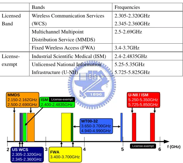
(13) non-LOS environment. In the 2-11GHz operation band, IEEE 802.16e adds mobility and enables applications on notebooks and PDAs in the frequency range of 2-6GHz [2]. The band range does not unified from country to country, but there are some usually referenced bands from USA as Table 1.1:. Table 1.1: WiMAX reference bands in 2-6GHz range. Licensed Band. Licenseexempt. Bands. Frequencies. Wireless Communication Services (WCS). 2.305-2.320GHz 2.345-2.360GHz. Multichannel Multipoint Distribution Service (MMDS). 2.5-2.69GHz. Fixed Wireless Access (FWA). 3.4-3.7GHz. Industrial Scientific Medical (ISM). 2.4-2.4835GHz. Unlicensed National Information Infrastructure (U-NII). 5.25-5.35GHz 5.725-5.825GHz. MMDS 2.150-2.162GHz ISM License-exempt 2.500-2.690GHz 2.400-2.4835GHz. U-NII / ISM 5.250-5.350GHz 5.725-5.850GHz. WT00-32 3.650-3.700GHz 4.940-4.990GHz. 2 US WCS 2.305-2.320GHz 2.345-2.360GHz. 3. FWA 3.400-3.700GHz. 4. 5. License-exempt. 6. f (GHz). Figure 1.1: Bands for WiMAX Applications in 2-6GHz range. In this thesis, we focus on the first band of the WiMAX 2.3-2.7GHz. In this band, the WCS, ISM and higher part of MMDS applications are covered.. 3.
(14) 1.2.2 Receiver Specifications In the IEEE 802.16-2004 standard [3], there are four air interfaces which operates in frequency band below 11GHz: WirelessMAN-SCa, WirelessMAN-OFDM, WirelessMAN-OFDMA and WirelessHUMAN. In this thesis, WirelessMAN-OFDM and WirelessMAN-OFDMA interfaces are focused.. A. Sensitivity and maximum input From the IEEE 802.16-2004 document, the required BER (bit error ratio) shell be less than 10-6 in both WirelessMAN-OFDM and WirelessMAN-OFDMA interfaces. The receiver maximum input signal is -30dBm in both two interfaces, too. But other receiver requirements, such like sensitivity and adjacent channel rejections, are different between interfaces. Following the IEEE 802.16e-2005 document [4], assuming 5dB implement margin and 8dB NF for receiver chain, the input sensitivity specifications in OFDM interface shell be:. RSS = −101 + SNRRx + 10 ⋅ log( Fs ⋅. N used N subchannels ) ⋅ N FFT 16. (1). Where SNRRx: the receiver SNR in dB, depends on modulation scheme and coding rate. Fs: sampling frequency in MHz, Fs = floor (n ⋅ BW 8000) × 8000 . Nused: Number of used subcarriers, default is 200. NFFT: Smallest power of two greater than Nused. Nsubchannel: the number of allocated subchannels (default 16 if no subchannelization used). 4.
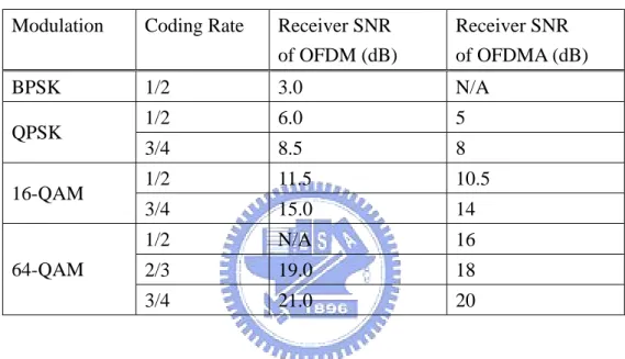
(15) From Table 1.2, when the BPSK modulation and 1/2 coding rate are used, the SNR reaches a minimum number as 3dB. The minimum channel bandwidth is 1.5MHz, n=86/75 for 1.5MHz BW. Combine these conditions into (1), we can derive the minimum input signal shall be -96.7dBm.. Table 1.2: Receiver SNR assumptions of WirelessMAN-OFDM and WirelessMAN-OFDMA Interfaces Modulation. Coding Rate. Receiver SNR of OFDM (dB). Receiver SNR of OFDMA (dB). BPSK. 1/2. 3.0. N/A. 1/2. 6.0. 5. 3/4. 8.5. 8. 1/2. 11.5. 10.5. 3/4. 15.0. 14. 1/2. N/A. 16. 2/3. 19.0. 18. 3/4. 21.0. 20. QPSK 16-QAM. 64-QAM. On the other hand, use the same conditions of implement loss and NF above, the input sensitivity specification of OFDMA shall be:. RSS = −114 + SNRRx − 10 × log10(R ) + 10 ⋅ log10(. Fs ⋅ N used ) + impLoss + NF N FFT. (2). Where R: The repetition factor (1, 2, 4 or 6). imploss: implement loss, default is 5dB. NF: noise figure, default is 8dB.. Table 1.2 also describes the receiver SNR assumptions in OFDMA interface. When QPSK modulation and 1/2 coding rate is used, SNR has a minimum number as. 5.
(16) 5dB. The minimum channel bandwidth is 1.5MHz, n=86/75 for 1.5MHz BW, Nused=420, and the largest R is 6. Combine these worst conditions into (2), we can derive the minimum input signal shall be -102dBm. It is lower than the sensitivity of OFDM interface. Thus, the specifications shall meet this -102dBm receiver sensitivity requirement in our LNA design.. B. Adjacent and non-adjacent channel rejection The adjacent and non-adjacent channel rejection requirement of both interfaces is listed in Table 1.3. The requirement is identical in both interfaces.. Table 1.3: Adjacent and non-adjacent channel rejection Modulation. Adjacent Channel Nonadjacent Channel Rejection (dB) Rejection (dB). 16-QAM 3/4. 11. 30. 64-QAM 2/3. 4. 23. The input third order intercept point (IIP3) is a linearity factor of receiver, and it can be derived from: IIP3 =. 3 ⋅ Pblocke r − Pdesired + SNRrequired 2. (3). Where Pblocker: the adjacent or non-adjacent channel blocker level in dB. Pdesired: the desired signal, which is 3dB above the sensitivity.. From (3), the maximum IIP3 of receiver in OFDM 16QAM 3/4 modulation is -18dBm. The P1dB specification can be obtained by subtracting 9.6dB from the IIP3 requirement. [5]. 6.
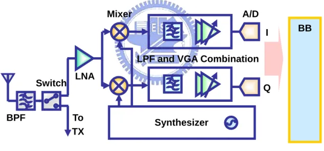
(17) 1.2.3 Receiver Architecture Figure 1.2 illustrates the system architecture of WiMAX receiver. Recently the direct conversion structure for receiver is very popular and has presented in many literatures. This structure is also adopted in this research. There are many advantages of direct conversion structure, such as reducing image rejection devices and simplifying integration of blocks, which can help to save power consumptions and to realize the system-on-chip integration. On the other hand, the drawbacks of direct conversion structure are problems of DC-offset, I/Q mismatch, even-order distortion and flicker noise.. Mixer. A/D I. BB. LPF and VGA Combination Switch. BPF. LNA Q To TX. Synthesizer. Figure 1.2: System architecture of WiMAX receiver. In the receiver architecture, a band pass filter and a Tx/Rx switch are the first two blocks. The proposed LNA is the next block, with mixer blocks in separated I/Q paths following. After the mixer blocks, several variable gain amplifiers and a low pass filter stage are combined as an analog baseband block. Analog-digital converter block is at the last and connects to baseband. Synthesizer offers the local oscillate frequency. 7.
(18) signals to mixers.. 1.2.4 LNA Specifications Calculation From previous section, we know the receiver sensitivity is -102dBm, and the maximum input signal is -30dBm. Therefore the receiver dynamic range can be derived as -102-(-30) = 72dB. This range is derived on the condition of NF<8dB. IIP3 of receiver is also derived as -18dBm. To design the proposed LNA, the specifications of LNA (and other blocks) shall be calculated from these receiver requirements. The distributions of dynamic range (gain) and NF can be derived by the Friis’ equation [6]: NFtot = 1 + ( NF1 − 1) +. NFm − 1 NF2 − 1 +L+ A1 A1 L A(m −1). (4). Where NFtot: receiver overall noise figure. NFn: noise figure of nth block. An: power gain of nth block.. And the distribution of dynamic range and IIP3 can be derived by following equation [5]:. α 12 α 12 β12 1 1 ≈ + + +L AIP2 3 AIP2 3,1 AIP2 3, 2 AIP2 3,3 Where AIP3: total input IP3. AIP3,n: input IP3 of nth block.. α1, β1…: gain of 1st, 2nd…blocks.. 8. (5).
(19) The 72dB dynamic range and the -18dBm IIP3 give a tough standard for circuit implementation. In the receiver architecture, most contribution of dynamic range is given by the analog-baseband circuit, especially variable gain amplifier (VGA). But it is a great challenge for overall 80dB range which offers only by VGA within reasonable power consumption. By introducing dual gain mode method to receiver front-end, the dynamic range will split into two modes: high gain mode for small input power signal, and low gain mode for large input power one. It can relax not only the gain range, but the linearity requirements (especially p1dB) of analog-baseband circuit. If input signal power is small, high gain mode will turn on for low noise and good signal quality. If input signal power is large, low gain mode will operate for preventing signal blocking. The specifications of blocks list on table 1.4. The overall NF setting to 7dB, 1dB lower than [4], is for more easily passing the system verification.. Table 1.4: The receiver block specifications BFP. Switch. LNA. Mixer HPF. LPF. VGA. Unit. Gain(H). -1. -1. 17. 8. 10. -3. 70. dB. Gain(L). -1. -1. 8. 8. 0. -3. 25. dB. NF. 1. 1. 2.5. 10. 15.1. 21. 21. dB. IP1dB(H). -15. 0.25V. 0.31V. 0.5V. 0.35V. dBm/V. IP1dB(L). -5. 0.25V. 0.31V. 0.5V. 0.35V. dBm/V. IIP3(H). -4.5. 0.84V. 1.02V. 1.68V. 1.17V. dBm/V. IIP3(L). 5.5. 0.84V. 1.02V. 1.68V. 1.17V. dBm/V. 4.86. dB. IIP3(H), cas. -24.54. dBm. IIP3(L), cas. -8.89. dBm. NF, cas. 6.86. 5.86. 9.
(20) 1.3 Previous Techniques of Multi Gain Mode LNA The dual or multi gain mode method is very popular for dynamic range extension. This method can be implemented to circuit by several techniques which have been presented in many literatures [7-11]. These techniques can be distributed in four types: load switching, current splitting, bias control and core switching, and they will be introduced in following sections.. 1.3.1 Load Switching Type The basic LNA can be split to three stages: input stage, gm stage and output stage, as illustrated in Figure 1.3. The first stage is input stage, with a matching network in it. The Gm stage is constructed by transistors in most of LNA circuit. Load and outmatching network are in the output stage. Since the gain is equal to gm multiplies load, if the load can be changed by switch, the gain of LNA will be changed, too.. Input Stage. Gm Stage. Output Stage Gain = gm * load. Input matching network. Transistors. Output matching network. Figure 1.3: Basic LNA stages. Figure 1.4 shows an example LNA circuit which is using the load switching technique [7]. The circuit is designed for dual-band operation. Two input matching network and input transistor sets are for different bands. Two inductors L2, L3 and one transistor M4 forms a switchable resonator, which is as a load in output stage. The. 10.
(21) LNA has no output matching network because the LNA output directly links to mixer in original circuit. When Vctrl is low, M4 is off and the resonator (forms by L2, L3 and parasitic capacitors from M4) resonates at 2.4GHz. On the other hand, when Vctrl is high, M4 is on and the resonator (L3 is bypassed) resonates at 5.15GHz. Thus the high gain mode can be obtained by setting resonate frequency of resonator to operation frequency, and low gain mode can be obtained by setting different resonate frequency. This concept is illustrated in Figure 1.5.. VDD Rg V ctrl L3. M4. L2 Vbias. C1. Vout. M3. Cbp Vin for 2.4GHz. Vin for 5.15GHz M1 M2 Lpcb1. Lpcb2 L1. Figure 1.4: Schematic of load switching LNA [7]. There are several advantages in this techinque. First, the load switch controls both band and gain mode. Second, because the switch is just change the load in output stage, the operation points of transistors in the core circuit is almost unchanged. The cascode structure in core circuit also helps the reverse isolation. Thus the impacts on. 11.
(22) Power Gain (dB). Vctrl=low. Vctrl=high. 20. High gain mode Low gain mode. 10. 2.4. 5.15. f (GHz). Figure 1.5: Load switching concept in [7]. power consumption, NF and input matching are negligible. On the other hand, two major drawbacks are in this circuit. First, voltage room of loads is very small due to low VDD and cascode structure. In this situation, M4 shall work in triode region to save the voltage room. But unless Vctrl is higher than VDD+Vth, M4 is impossible to operate in triode region. In [7], Vctrl is switched between VDD and 2VDD. It gives complexity of designing DC power supply circuit, which has to supply 2VDD. The other one is that the gain variation is sensitive due to parasitic effects.. 1.3.2 Current Splitting Type Figure 1.6 shows an example variable gain LNA using current splitting technique [8]. Bias circuit is not shown. When the LNA is set in high gain mode, transistor Q4 is off, and all current of Q2 flows to Q5. If Q4 is on, the current of Q2 will be split to Q4, and there is only a small fraction of current (via Q3 and Q6 in this circuit) passes to output, so gain can be reduced. The advantage of the circuit [8] is that the gain step can be accurately created by setting the ratio of Q2 and Q3 sizes. In the later applications of this technique, Q3, Q6 path is deleted and Q4 route becomes multiple for more gain steps [9]. But the major. 12.
(23) problems of this technique are power wasting and high NF in low gain mode. The second problem is mitigated in [9], but the power consumption is still an important issue.. VDD1 L1. R5 C5 VDD2. Vout C2 Vctrl. Vin. Q4. Q6. Q5. Q2. Vbias. Q3. Figure 1.6: Schematic of current splitting LNA [8]. 1.3.3 Bias Control Type The bias control technique controls gain by changing gm of transistors in Gm stage, and gm control can be realized by adjusting bias voltage. Figure 1.7 gives an example circuit using bias control technique [10]. In this circuit, both M1 and M2 are common-source configurations. Gain control is achieving by adjusting the bias voltage of M2 [10]. The control range is analogical with the bias range which keeps M2 in active region. The advantage of this technique is that the input and output return loss (S11 and S22) are not degraded during the gain changes. And the peak curves of gain versus. 13.
(24) frequency are almost at the same frequency. There are some drawbacks in this technique, too. The control range is smaller than other techniques due to the active range of M2 is limited. Analogical controlled bias circuit also gives complexity to circuit design.. VDD LD C3. Vout c. Vctrl M2 C1. C4 C2. LM. Vin. M1 LG LS. Figure 1.7: Schematic of bias controlled LNA [10]. 1.3.4 Core Switching Type The core switching technique is realized by switching signal paths in the gm stage. The signal paths can through different transistors, or through parallel transistors which are just for changing total width of them. But the signal paths are limited between input and output, no branch (like current splitting) links to any other point. Figure 1.8 shows an example circuit using parallel transistors switch [11]. The parallel transistors M2 to M5 are replaced common-gate transistor of cascade structure. There are four modes, depending on number of switching-on transistors.. 14.
(25) Figure 1.8: Schematic of core switching LNA [11]. In the load switching technique, it is hard to implement a CMOS switch, due to limited voltage room and additional parasitic effects. Core switching technique combines the switch and original devices, and it doesn’t consume more voltage room or waste more current. The control signals come from baseband, so they are programmable, and complex bias circuit is not needed. Input matching may have a little variation between different modes, due to DC current and gm changing, but it is not severe. The major problems of this technique are P1dB improvement in low gain mode, and NF variation between different gain modes. Although it already has P1dB improvement in low gain mode, it is still not enough, because cascode structure is not changed. The current variation between different gain modes makes different NF performances, and it is not fit to the NF requirement of proposed circuit.. 15.
(26) 1.3.5 Summary The advantages and drawbacks of techniques mentioned before are listed in Table 1.5. This table can help to develop a new multi-gain mode topology for WiMAX system. The comparisons of gain, P1dB, current and NF variations between high gain mode and low gain mode (loss mode is not included) are listed in Table 1.6. In this table, it can be found that the P1dB range is larger in core switching technique, and the NF variation is smaller in modified current splitting technique (this modified technique includes concept of load switching one). These two features are important references in designing the proposed circuit.. 1.4 Organization The organization of this thesis is overviewed as following: Chapter 2 presents the design methodology of Dual-mode LNA. In this chapter, a new topology for wider dynamic range is proposed. Chapter 3 presents the implemented circuit with UMC 0.13μm CMOS technology and measurement results. For shortening the system verification time, a behavior model of dual-gain mode LNA is constructed and demonstrated in Chapter 4. Chapter 5 concludes with a summary of contributions and the future works.. 16.
(27) Table 1.5: Advantages / disadvantages of multi gain mode techniques Type of techniques. Example Advantages Circuit. Disadvantages. Load switching. [7]. (1) Can control both band and gain modes (2) Impacts on power consumption, NF and input matching are negligible. (1) Switch control voltage may higher than VDD (2) Gain variation is sensitive due to parasitic effects. Current splitting. [8-9]. Gain step can be accurately created by setting the ratio of transistor sizes. (1) Power wasting problem (2) High NF in low gain mode. Bias control. [10]. (1) S11 and S22 do not degrade during gain changes (2) Peak curves of gain versus frequency are almost at the same frequency. (1) Control range is smaller (2) Complex analogic control circuit. Core switching. [11]. (1) No extra voltage room or current needed (2) Control signals are programmable. (1)P1dB improvement is not enough in low gain mode (2)NF variation between different modes. Table 1.6: Gain, P1dB, current and NF comparison of multi gain mode techniques Technique. Ref. Gain vari. (dB). P1dB vari. (dB). Current vari. (mA). NF vari. (dB). Freq (GHz). Process. Load Switching. [7]. 17. 4. 0. w/o. 2.4. 7. 2.5. 0. w/o. 5.15. 0.18μm CMOS. Current Splitting. [9]. 14.4. 0. 0.02. 2. 0.9. 11.7. 0. 0.01. 1.2. 2. Bias Control. [10] 8. w/o. w/o. 2.2. 5.7. 0.18μm CMOS. Core Switching. [11] 11. 5.4. 0.86. 2.95. 2.4. 0.18μm CMOS. 17. 0.5μm BiCMOS.
(28) Chapter 2 Dual-gain Mode LNA Design In this chapter, a CMOS LNA with dual-gain mode for WiMAX application is presented. Section 2.1 describes design concepts for high dynamic range of LNA for WiMAX applications. Section 2.2 introduces the dual-gain mode LNA topology. Based on this topology, a circuit design by 0.13μm process is shown in section 2.3. Section 2.4 provides simulation results of this circuit.. 2.1 Design Concepts From previous chapter, the specifications of dual-gain LNA are defined. The goal of this work is to design an LNA which can satisfy defined specifications. The LNA circuit has to be low noise figure, high gain and high linearity performance for wide dynamic range demand. Well matching networks can help to keep high power transfer efficiency between blocks. Moreover, for trend of minimizing size and power consumption in designing consumer electronic products nowadays, IC layout area and power consumption are more important issues than before. It is a great challenge to balance effects of these issues, due to tradeoffs or conflicts between some of them. If LNA circuit has to be with high gain to reduce. 18.
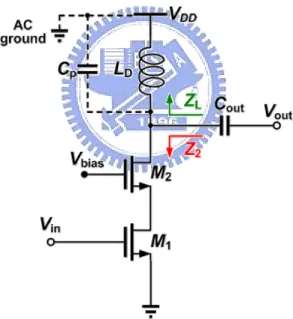
(29) noise, raise gm is an effective way, but power consumption is raised, too. On the other hand, high gain LNA is suitable for small input signal, but when input signal is large, blocking problem will become seriously. The specifications in previous chapter declare that the requirement of gain and linearity is very severe. Even the dual-gain mode method will be used to release trade-off between gain and linearity specifications, design of proposed LNA is still not easy. There are some popular techniques which can solve gain, linearity and noise problems respectively, and they will be discussed below.. 2.1.1 Gain Issue. Figure 2.1: A basic cascode CMOS LNA circuit. In the specification, the LNA power gain shall be more than 17dB in high gain mode. The common-source configuration is suitable for high gain, due to large effective load resistance as ro of transistor [12]. The cascode configuration, with much larger load than common-source one, can enlarge gain more efficiently and easily. Figure 2.1 depicts a basic cascode CMOS LNA circuit. The capacitor Cout is usually. 19.
(30) very large as a DC block, and it can be ignored for load calculation. The effective load equals to parallel impedances Z2 and ZL. ZL is impedance of resonator which is formed by load inductor LD and parasitic capacitance Cp. Z2 is impedance seen from the drain of M2, and it can be derived by following formula: Z 2 = ro 2 + (1 + g m 2 ⋅ ro 2 ) ⋅ ro1. (6). As mentioned before, the load is much larger than that of common-source only. But recently, for low power requirement in mobile devices, VDD is getting smaller, and it gives restrict of using cascode structure. Folded structure or multiple stages can avoid the voltage room restrict, but they have to consume more power.. 2.1.2 Linearity Issue The LNA input IP3 specification in low gain mode is 5.5dBm. Such high linearity requirement is not easy to conquer, and so linearity enhancement technique shall be introduced to proposed LNA. The multiple gated transistor technique [13] is simple to use. The technique comes from the drain current iDS versus vgs equation of a common-source amplifier: i DS = I DC + g m v gs +. gm ' 2 gm '' 3 v gs + v gs + L 2! 3!. (7). The vgs3 term in (7) plays an important role in the third order intermodulation distortion [13][14]. Thus we can use two or more paralleled transistors with different bias voltage (as multiple gated transistors) to cancel gm’’ term, and so the linearity of LNA can be enhanced. The concept of this technique is illustrated in Figure 2.2. In this technique, Vbias2 is lower than Vbias1 with a constant offset. M2 works in the sub-threshold region for positive gm’’ value by Vbias2, and so as to cancel gm’’ of M1.. 20.
(31) Figure 2.2: Schematic and gm’’ curve of multiple gated transistors technique. Because M2 works in sub-threshold region, the current of M2 is very small, and it gives no impact of power consumption. The gain will degrade in this technique, but it is not serious. The linearity improvement is not quite obvious in the first paper of this technique (3dB OIP3 improvement in [13]). A formula of small signal circuit derived in [15] gives a reason about the limit of original multiple gated transistors technique, where L is an inductor of source degeneration, and Z1 is input impedance: IIP3 =. ε = g m ' '−. 4 g m2 ω 2 LC gs 3ε 2( g m ') 3. (8). 2. C gs 1 gm + + j 2ωC gs + Z 1 (2ω ) j 2ωL L. (9). In the last term of (9), the contribution of nonlinearity is not only comes from gm’’. The original technique works only in low frequency operation, due to the last term is near to zero in low frequency. A modified technique which improves IIP3 near 20dB is presented in [16]. It uses a single tapped inductor for different source degeneration inductor values of two transistors. The circuit is depicted in Fig. 2.3. Because the inductor value seen from the source of M1 and M3 are different, they can be adjusted to cancel the last term of (9) (as gm second-order distortion). M1. 21.
(32) VDD L4. CB2 V out. Vbias2 M2. Vin. CB3. M3. M1 L2. CB1. L1 R3. R1. Vbias3. Vbias1. Figure 2.3: Schematic of modified derivative superposition LNA (Bias circuit and input matching network are not shown). works in active region, and M3 works in sub-threshold region. M2 forms the circuit as a cascode structure. The gain performance is good in this LNA, and gain degradation of using this techinique is smaller than 1dB. This technique is very useful for conquering requirements of proposed LNA.. 2.1.3 Noise Issue To be the first stage of receiver circuit, the noise problem is the most important issue in designing LNA circuit. Full integrated IC is popular for the system-on-chip design, but the low Q factor of on-chip inductor gives a challenge to it. The source degeneration technique is widely used for input matching (Figure 2.4). In this technique, the input signal is directly through the inductor Lin. If the Q factor of Lin is small, there will be a parasitic resistance on it, and it generates noise. Because the. 22.
(33) inductor is just after the input port, it gives serious impact to LNA noise performance. Thus the input inductor shall be carefully designed.. Figure 2.4: The source degeneration technique. The size selection of common-gate transistor is also an issue of noise performance. The cascode stage has a smaller impact on the overall NF than input stage [17], but it plays an important role when the input stage is optimized. The [17] paper gives an reference of selecting the size of common-gate transistor. The specification decided the same NF requirement for dual gain modes. Thus the degradation of NF performance in low gain mode has to be avoided. In the [9] circuit which is introduced in previous chapter, the noise variation between different gain modes is smaller. This technique can be an important design reference for the noise issue.. 2.2 Dual-gain Mode Topology 2.2.1 Design Footprints From the specifications in previous chapter, the LNA has to be designed with dual-gain mode. Two modes shall be integrated in one circuit to save chip area. To. 23.
(34) realize this requirement, two circuits for different modes are designed first to see the common points. If the LNA can split into two circuits, one is designed for high gain mode and the other is for low gain mode, the design will be quite simple and no new techniques needed. Cascode configuration can be used for high gain requirement in high gain mode circuit. Low gain mode does not use cascode configuration for larger voltage room of common-source stage. Multiple gated transistor technique can be used for high linearity requirement in both gain mode circuits. The first designed structures of two mode circuits are illustrated in Figure 2.5. The high gain mode circuit structure is just the same as the circuit in [18].. (a). (b). Figure 2.5: First designed LNA (a) for high gain mode; (b) for low gain mode.. Although the optimizations of these two circuits may lead to different sizes of components, the major difference between them is the existence of M2 transistor. If M2 transistor can be “short” by giving different bias in high gain mode circuit, these two circuits can be merged into one.. 24.
(35) The bias control and core switching techniques in [10][11] offered good references here. Adjusting Vbias2 may cause obviously gain variation, even the gain can lower than the circuit without cascode structure in Figure 2.5(b). But the linearity performance will be seriously degraded; even though the gain is already lower. Complex bias control circuit is another drawback which is mentioned before. On the other hand, the core switching technique does not degrade linearity performance during gain control, but the gain range is quite small. The LNA, which combines core switching technique (2 bits only), is illustrated in Figure 2.6.. Figure 2.6: The LNA circuit with core switching technique. In Figure 2.6, if the transistor M2B can short vd1 and vd2 two points when it is on (and M2 shall be off), the merged circuit can be realized. Vbias2B shall bias M2B into triode region for the minimum voltage room consumption. M2B works in triode region when (Vbias2B — vd2) is smaller than Vt3. But vd2 is nearly to VDD here, M2B is impossible to operate in triode region except Vbias2B can be larger than VDD. The. 25.
(36) over-VDD bias circuit is major problem of this structure.. 2.2.2 The Proposed Dual-gain Mode LNA Topology The transistor M2B in Figure 2.6 can work as a real switch if PMOS is used. The schematic of proposed LNA is depicted in Figure 2.7. The input, output matching networks and source degeneration inductor is added in the circuit. The PMOS M2B can easily bias in the triode region by setting Vbias2B to zero, since the Vsg of M2B reaches almost as VDD voltage, and Vsg-|Vth| is still much larger than Vsd of M2B. The circuit operation and analyses are described in following subsections.. Figure 2.7: The proposed Dual-gain mode LNA circuit schematic. A. Circuit structure and operation. The proposed LNA circuit can be split into 4 stages: input matching stage, gm. 26.
(37) (Multiple gated transistors, MGTR) stage, switching stage and output matching stage. Capacitors CB1, CB2 and CB3 are with large size as DC blocks. Resistors R1, R3 are also with large size, and they are for supplying bias without degrading RF signal. The input matching stage is formed by input inductor Lin and source degeneration inductor LS. The gm stage is formed by M1 and M3 transistors. It uses the MGTR [13] (or Derivative Superposition named in [16]) technique to meet the IIP3 requirement. M1 works in active region and off, and M3 works in sub-threshold region. The biases of M1 and M3 can be adjusted for the best IIP3 performance. The switching stage is the major contribution of this new technique. In high gain mode, M2 is on by setting Vbias2 to high, and Vbias2B is also set to high to turn off M2B. Thus the circuit becomes to cascode configuration, and high gain can be realized. On the other hand, M2 is off by setting Vbias2 to low, and Vbias2B is also set to low to turn on M2B in low gain mode. Because in the same mode, the voltage level of Vbias2 and Vbias2B are the same, two bias points can be combined into one, and the control signal can be given from baseband. The M2B works in triode region, which Ron is small, and it does not consume much voltage room. The voltage at vd1 will be much higher than in the cascoded high gain mode, so the swing in the gm stage can be larger. The output matching stage contains load inductor Lload, matching network Lout and Cout. The load inductor Lload and parasitic capacitances (from M2 and M2B) form a resonator, which shall resonate at the center frequency of operating band (2.5GHz).. B. Circuit analysis in input matching issue. The degeneration inductor LS can help to make real part of input impedance to 50Ω, as following equation describes:. 27.
(38) ⎡⎛ 1 ⎞ ⎛ g L 1 ⎟⎟ // ⎜⎜ sLS + Z in = sLin + ⎢⎜⎜ + m1 S sCT 1 CT 1 ⎣⎝ sCT 3 ⎠ ⎝. ⎞⎤ ⎟⎟⎥ ⎠⎦. (10). ⎡ ⎛ 1 ⎞⎤ ⎟⎟⎥ CTX = C gsX ⎢1 + g mX ⎜⎜ ro1 // ro 3 // g m 2 ⎠⎦ ⎝ ⎣. (High gain mode). (11a). CTX = C gsX {1 + g mX [ro1 // ro 3 // (ron 2 + RL )]}. (Low gain mode). (11b). where. Inductor LS locates between source of the transistor M1 and ground. CT represents capacitor with Cgs and Miller effect of Cgd. Because loading at the drains of M1 and M3 is different between two gain modes (by whether the circuit is cascoded or not), CT will change their value. The variation of CT can be controlled by designing different gm for different modes. gm does not only effect CT, but directly link to the real value of Zin. The optimum gm should keep Zin to 50Ω and minimize the variation between two gain modes. It can be obtained by carefully designing sizes and biases of transistor M1, M3.. C. Linearity issue. The IIP3 equation derived in [16] can be modified for this new technique without taking the inductor between source of M3 and ground (as L1 in [16]) into account (only gm stage): IIP3 =. where. 4 g m2 1ω 2 [ LS C gs1 ]. (12). 3ε. [. ]. ε = 2 g m' ' 3 (1 + jωLS ) 1 + (ωLS g m1 )2 + g m' ' 1 −. 2( g m' 1 ) 2 j 2ωLS g m1 3g m1 1 + j 2ωLS g m1. (13). The impact of not using the inductor L1 is that the second-order distortion may not be cancelled as well as before. The first and third terms of (13) are both raised their value. But since the first and third terms are with different signs, and the numerator of (12) is also raised when the denominator ε is raised, the impact of not using L1 is quite. 28.
(39) small. By the way, the absence of L1 gives a convenience of designing if the value of L1 is hard to implement.. D. Noise issue. The MGTR Fmin derivation in [16], based on assumption of long channel device but without degeneration inductor, is given by: Fmin ≈ 1 +. where. g g,X =. 2 2 γ 1 g d 0,1[δ 2 g g ,3 + δ 1 g g ,1 (1 − c1 )] g m1. 4ω 2 (CoxW X Leff ) 2. ,. 45 g d 0, X g d 0,3 =. I D3. φt. g d 0,1 = 2μCox. , c1 =. * ing ,1 ⋅ ind ,1 2 2 ing ,1 ⋅ ind ,1. W1 I D1 Leff. (14). ,. (15). In this equation, the drain currents in both M1 and M3 transistors play important roles in noise performance. Because sizes of transistors are unchanged between high and low gain modes, the variation of NF between different gain modes will follow the value of drain currents. By the way, the switching stage structure is different in two modes. Even the currents condition will satisfy the minimum NF variation, the noise contribution of switching stage is still greater in low gain mode, due to saturation mode of M2B and less gain of gm stage. The problem can be reduced by giving a little more current to M3 which is working in sub-threshold region (Fmin will rapidly increases with vgs falling below vth [16].).. 2.3 Circuit Design This section introduces the size selection of each component. The UMC 0.13μm RF CMOS model is applied to this design, and the ADS RFDE simulation tool is used. 29.
(40) for design supporting.. 2.3.1 Input Matching Stage The size of source degeneration inductor can be decided from three issues: First, the real part of Zin equals to gmLS/CT in (10). Second, large size of LS will degrade gain performance. The last one is the adjustment of linearity performance optimization. The size is usually smaller than 1nH in many literatures, and it needs to realize by bondwire. But the circuit design here is fully-integrated, and such small inductor is also supported in the UMC 0.13μm model. The LS size is decided as 0.37nH. To cancel the image part of input impedance in (10), the input inductor Lin shall be [1/(ω2Cgs)]-LS, and it is near to 10nH. The quality factor affects the noise performance of LNA very much, since the parasitic resistance of Lin generates noise at the initial stage. It can be proved by Friis’ equation. In the circuit the Lin is designed as 5.8nH. The sizes of DC blocks and resistors are designed for not disturbing RF signal transmission. DC block is better of larger size, but it occupies too large area on the chip. The 4.57pF size of DC blocks is decided for smaller area and less degradation of signal coupling. The resistors value is nearly 10kΩ.. 2.3.2 gm (MGTR) Stage Designing the size of transistors M1 and M3 shall consider following issues: Cgs for input matching, gm for gain, and gm’’ for MGTR technique. To make 17dB gain in high gain mode, M1 size shall be large enough for large gm. But if M1 size is too large,. 30.
(41) DC current as well as power consumption will be a problem. On the other hand, M3 size has to be much larger than M1. Power issue here is not serious as M1, due to the current is very small. Small current makes small variation, so the positive gm’’ value is smaller than negative gm’’ offered by the same size M1. Moreover, the optimum linearity performance points are different between two gain modes. It needs to be balanced in M3 size choosing. The final sizes (width) of M1 and M3 are decided as 96μm and 240μm, respectively.. 2.3.3 Switching and Output Matching Stage The parasitic capacitances of M2, M2B and the load inductor Lload form a load resonator. It shall resonate at the center frequency of the band. Because the size of M2 and M2B gives a directly connection to parasitic capacitances, this is an issue for designing the size of M2 and M2B. Moreover, the M2B size shall be larger for lower Ron, so that the consumption of voltage room by M2B will be smaller. The size of M2 and M2B are decided as 192μm and 240μm, respectively. Lload is designed as 5.34nH. Besides the Lload and parasitic capacitances, capacitor Cout and inductor Lout are also a part of output matching. Cout as 409fF, and Lout as 2.96nH are designed. All the component sizes are listed in Table 2.1.. 2.4 Simulation Results The circuit simulation is accomplished with ADS RFDE simulation tools. The parasitic capacitances in layout are considered in simulations. Table 2.2 shows the DC simulation of this circuit. Table 2.3 presents S-parameter simulation results, with results at 2.5GHz and the worst case in the band. Table 2.6 describes harmonic. 31.
(42) simulation results, under the conditions of that reference input power = -40dBm, 2.5GHz operating frequency and 10MHz offset of two tone test. Figure 2.8 to 2.11 show the curve of S-parameter and harmonic balance simulations results in 1-4 GHz.. Table 2.1: The component size list of proposed LNA Transistors. μm / μm. Inductors. nH. M1. 96 / 0.12. Lin. 5.790. M3. 240 / 0.12. LS. 0.370. M2. 192 / 0.12. Lload. 5.344. M2B. 240 / 0.12. Lout. 2.957. Capacitors. pF. Resistors. kOhm. CB1. 4.568. R1. 9.96. CB2. 4.568. R2. 9.96. CB3. 4.568. Cout. 0.409. Table 2.2: DC simulation results Post-Sim. ID (mA). Power (mW) Vbias1 (mV). Vbias3 (mV). HG mode. 7.49. 8.99. 540. 360. LG mode. 6.15. 7.38. 500. 280. Table 2.3: S-parameter simulation results Post-Sim. S21 (dB). NF (dB). S11 (dB). S22 (dB). S12 (dB). HG mode (2.5G) 17.69. 1.95. -8.34. -4.97. -35.7. Worst case. 17.22. 2.08. -6.44. -4.17. -35.46. HGM Spec. 17. 2.5. -15. -15. LG mode (2.5G). 8.56. 2.12. -21.98. -6.79. -20.55. Worst case. 7.29. 2.29. -16.92. -6.46. -20.15. LGM Spec. 8. 2.5. -15. -15. 32.
(43) Table 2.4: Harmonic Balance simulation results Post-Sim. IIP3 (dBm). IIP3 w/o MGTR (dBm). P1dB (dBm). HG mode. 1.443. -2.11. -15.48. HGM spec. -4.5. LG mode. 5.376. LGM Spec. 5.5. (a) S11. -15 1.076. -8.04. -5. High gain mode Low gain mode. (b) S22. Figure 2.8: Smith charts of S11 and S22. (a) S11. High gain mode Low gain mode. (b) S22. Figure 2.9: S11 and S22 curves in dB. 33.
(44) (a) S21. High gain mode Low gain mode. (c) NF. (b) S12. (d) P1dB. Figure 2.10: S21, S12, NF, P1dB simulation results. (a) High gain mode. (b) Low gain mode. Figure 2.11: HB IIP3 simulation results. 34. output IM3 IM3 w/o MGTR.
(45) Chapter 3 Implementation and Experimental Results In this chapter, the proposed circuit is implemented and measured. The circuit is implemented by the UMC 0.13μm process. Section 3.1 addresses layout consideration. The proposed technique tapes out two times. Section 3.2 presents measurement results and analysis of DUT 1, and the new version DUT 2.. 3.1 Layout Consideration RF circuit is very sensitive to the parasitic effects. The signal path shall be carefully arranged by following considerations. First, the parasitic resistance shall be avoided. The narrow path or vias generate more parasitic resistance, and thus they may seriously degrade the noise performance. Second, the distance between two paths or components shall be larger to avoid mutual inductance or parasitic capacitance. Third, to avoid the coupling noise from noisy substrate, the top metal layer is used for signal path. The last consideration is that the path shall be as short and straight as possible. If there is a branch on the path, the distance of two paths shall be designed to. 35.
(46) the same to avoid phase variation. In the component arrangement, it shall be arrange as symmetric as possible for same components, and thus the process variation between these components can be mitigated. Also, the usage of maximum finger number of transistor is suggested by [19]. Large finger number leads to lower process variation and better model fitting. In addition, the MOS capacitors are used at each DC port. They work as bypassing capacitors. The noise coming from biases can be filtered by them. Figure 3.1 illustrates the layout of the DUT 1. The layout is accomplished with Cadence Virtuoso editor. The die area is 0.85×1μm2.. Figure 3.1: Layout of DUT 1. 3.2 Measurement and Analysis 3.2.1 Measurement Setup The measurement is on wafer testing with NDL support. The setup of the. 36.
(47) measurement is described in Figure 3.2. ESG, Noise analyzer, Network analyzer and Power spectrum analyzer are used. The DC 6pin probe is used for 5 biases and 1 ground. Two RF GSG probes are used for input and output.. Figure 3.2: Measurement setup. 3.2.2 Measurement Results The measurement results are presented in following tables and figures. Table 3.1 describes the DC measurement results. Table 3.2 lists the S-parameter and NF results. Table 3.3 presents harmonic balance results. The post-simulation results of DUT 1 are also listed in these tables for comparison. Figure 3.3 to 3.5 show the curves of measurement and post-simulation.. 37.
(48) Table 3.1: DC measurement results Measured ID (mA). Post-Sim ID (mA). Vbias1 (mV). Vbias3 (mV). HG mode. 7.375. 2.28. 540. 360. LG mode. 6.249. 10.49. 500. 280. Table 3.2: S-parameter measurement results S21 (dB). NF (dB). S11 (dB). S22 (dB). S12 (dB). HG mode (2.5G) 11.8. 2.465. -5.193. -6.632. -34.43. Worst case. 10.01. 2.8. -3.876. -5.647. -33.56. Post-Sim (2.5G). 17.611. 2.668. -12.757. -5.727. -37.627. HGM Spec. 17. 2.5. -15. -15. LG mode (2.5G). 8.452. 2.185. -4.913. -7.808. -26.56. Worst case. 6.62. 2.44. -4.124. -7.391. -25.51. Post-Sim (2.5G). 8.625. 2.774. -12.064. -6.494. -22.629. LGM Spec. 8. 2.5. -15. -15. Table 3.3: Harmonic balance measurement results Pre-Sim. IIP3 (dBm). IIP3 w/o MGTR (dBm). P1dB (dBm). HG mode. -2.073. -1.331. -7.1. Post-Sim. 4.895. -2.964. -16.12. HGM spec. -4.5. LG mode. 2.761. 1.414. -11.46. Post-Sim. 5.973. 1.3. -7.94. LGM Spec. 5.5. -15. -5. 38.
(49) (a) HGM S11. (b) HGM S22. (c) HGM S21. (d) HGM S12. (e) LGM S11. (f) LGM S22. (g) LGM S21. (h) LGM S12. Figure 3.3: S-parameter measurement and post-simulation results. 39.
(50) (a) High gain mode. (b) Low gain mode. Figure 3.4: NF measurement and post-simulation results. (a) HGM IIP3. (b) LGM IIP3. (c) HGM P1dB. (d) LGM P1dB. Figure 3.5: Harmonic balance measurement results. 40.
(51) 3.2.3 Analysis In the measurement results, the DC current variation between post-simulation and measurement is the first problem. DC current is only one third of post-simulation in high gain mode, and 1.6 times of post-simulation in low gain mode. This variation affects gain and P1dB performances. Because the DC current is very low in high gain mode, gain is degraded, and P1dB performance is better. On the contrary, larger current in low gain mode results in higher gain and worse P1dB performance. The MGTR technique is used in this circuit, but the function is failed. There is almost no IIP3 improvement (even degrading) when using MGTR technique. To find the best IIP3, the bias voltage cab be rearranged. But In the both modes, the current variations are all very small when transistor bias is varying from 0V to VDD. It is impossible for such low variation, unless the transistor M1, M3, or both M1 and M3 are failed. The fail of transistors is the most likely reason of not fitting between measurement and post-simulation results. The reason of failure of transistors is that the bias voltage may not transfer to gate. Besides, the parasitic and EM effects may give some impact in measurement.. 3.2.4 New considerations From the previous experiences, a new device under test is designed for better performances. The noise and the gain performance are not fit to the specification in overall frequency bands. It is because the trade-off adjustment. For example, the input inductor shall be large for input matching, but the NF may serious degrade by low Q factor of large inductor. New DUT 2 gives more considerations of selecting these components. The layout of DUT 2 is illustrated in Figure 3.6. The comparisons of. 41.
(52) component sizes are listed in Table 3.4, and the comparisons of gain and NF simulations are illustrated in Figure 3.7. In addition, the line width of signal and bias path are designed to be larger to prevent signal path (or transistor) fail.. Figure 3.6: Layout of DUT 2. Table 3.4: Component size comparisons of DUT1 and DUT2 Width (μm). DUT1. DUT2. Lin. DUT1. DUT2. M1. 100. 96. size (nH). 8.756. 5.790. M3. 160. 240. Q (2.5GHz). 10.15. 10.55. M2. 200. 192. R (Ω). 13.546. 8.622. M2B. 300. 240. DUT1. DUT2. DUT1. DUT2. LS (nH). 0.370. 0.370. Lout (nH). 2.976. 2.957. Lload (nH). 5.326. 5.344. Cout (pF). 0.409. 0.409. 42.
(53) DUT 2 DUT 1. (a) HGM S21. (c) LGM S21. (b) HGM NF. (d) LGM NF. Figure 3.7: Gain and Noise comparisons between DUT1 and DUT2. 43.
(54) Chapter 4 Behavior Model of Proposed LNA Due to shorter time-to-market period nowadays, the behavior model of LNA circuit shall be constructed to reduce system verification time. In paper [20], a behavior model archives 0.79% error and 87% simulation time reduction. In this chapter, a behavior model of proposed LNA is constructed. Section 4.1 describes the issues of behavior model construction, and Section 4.2 is the simulation results.. 4.1 Issues of Behavior Model Construction The behavior model of LNA shall fit the following parameters: S-parameter, IIP3, P1dB and NF. The model can be constructed into three stages: input stage, gm stage and output stage. Input stage can be designed to fit S11 and noise performances. Gm stage can be constructed to fit S21 and linearity performances. Output stage can be arranged to fit S22. The behavior model is constructed by verilog-a language. In proposed verilog-a file, there are three ports (in, out, gnd) and two parameters (mode control, MGTR control). The two parameters can be controlled by simulators for different gain mode or MGTR operations.. 44.
(55) The model construction bases on the real components. For the passive components, there are some simple model can be used to substitute the complex model which offers by the foundry. The simple model is illustrated in Figure 4.1. In the figure, the shaded component is the most important one, and the size value is limited to equal to the revealed value.. Figure 4.1: Simple model of passive components. Figure 4.2: Input stage of LNA behavior model. The input stage model is presented in Figure 4.2. In the circuit, the bias resistor is. 45.
(56) ignored. The bias resistor just effects lower frequency reaction. The part A in the input stage is constructed all by passive components. Thus when the mode is changed, values in part A do not need to change. The Cgs1, R5 and Cgs3 form the model of transistors M1 and M3. The sizes of these components will change in different gain modes. The input noise sources, which dominate noise performance of LNA circuit, are placed at the gates of two transistors. The construction of output stage is most likely the input stage. Figure 4.3 shows the output stage. Only Cd and Rout need to change value when gain mode changes.. Figure 4.3: Output stage of behavior model. The structure of gm stage will change in different gain modes. In high gain mode, the gm stage will be formed by two small gm stages: common-source gm stage and common-gate gm stage. In low gain mode, the gm stage will be formed by common-source gm and a resistor Ron. The common-source gm can split to two paths to simulate the MGTR technique. In the common-source gm, it can be written as a 3-order equation to simulate the P1dB and IIP3 performance.. 46.
(57) 4.2 Simulation Results The comparisons of constructed behavior model versus the transistor level simulation results are illustrated in Figure 4.4 to 4.5. Table 4.1 lists the root mean square error values in the passband.. (a) HGM S11 and S22 (in dB). (b) LGM S11 and S22 (in dB). (c) HGM S11 and S22 (Real part). (d) LGM S11 and S22 (Real part). (e) HGM S11 and S22 (Image part). (f) LGM S11 and S22 (Image part). S11 (behavior level) S11 (transistor model) S22 (behavior level) S22 (transistor model). Figure 4.4: S11 and S22 Comparisons. 47.
(58) (a) HGM S21. (b) LGM S21. (c) HGM NF. (d) LGM NF. (e) HGM P1dB. (f) LGM P1dB Behavior model Transistor level. Figure 4.5: S21, NF and P1dB Comparisons. After the behavior model constructed, it can be used in the system co-simulation. The co-simulation platform shows in the Figure 4.6. We simulated with system block (which just lists some parameters), transistor level and behavior model in system co-simulation, and compared the performances of BER and simulation times. These. 48.
(59) simulations based on the condition of 1.5MHz channel bandwidth and QPSK 1/2 modulation. The simulation results are illustrated in Figure 4.7. The simulation time of behavior model is reduced to 84%.. Table 4.1: The RMSE values in the passband RMSE. High gain mode. Low gain mode. S11 (dB). 0.433. 0.434. S11 real (dB). 0.016. 0.016. S11 image (dB). 0.019. 0.014. S22 (dB). 0.339. 0.394. S22 real (dB). 0.013. 0.028. S22 image (dB). 0.019. 0.015. S21 (dB). 0.098. 0.4. NF (dB). 0.287. 0.34. Figure 4.6: WiMAX LNA co-simulation platform. 49.
(60) BER performances Transistor Level: 8.137x10⁻⁴ Behavior model: 2.181x10⁻⁵ System block: 7.978x10⁻⁴. Figure 4.7: System co-simulation results. 50.
(61) Chapter 5 Conclusions 5.1 Summary In this thesis, a 2.3-2.7GHz dual-gain mode CMOS LNA for WiMAX standard is implemented in a 0.13μm CMOS tech. The chip is fully integrated. A new technique of dual-gain mode LNA circuit is developed. The circuit needs only one common input matching network for different gain modes. The gain of LNA reaches 17dB in high gain mode, and IIP3 reaches 5.9dBm in low gain mode. A behavior model is constructed for facilitating design cycle.. 5.2 Future Works The WiMAX system supports many different channel bandwidths and modulations. The complete simulation of system verification takes a lot of time. In addition, the behavior model construction time is not short, more efficient way to generate model will be developed. Control and bias circuit will be co-designed with mixer, analog-baseband or baneband circuit design.. 51.
(62) Bibliography [1] [2] [3] [4] [5] [6] [7]. [8]. [9]. WiMAX Forum, http://www.wimaxforum.org/technology/ A. Amer, E. Hegazi, H. Ragai, “A Low-Power Wideband CMOS LNA for WiMAX”, IEEE TCS-II, Vol. 54, Issue 1, pp. 4-8, Jan 2007. IEEE, IEEE Standard 802.16-2004, Oct 2004. IEEE, IEEE Standard 802.16e-2005, Feb 2006. B. Razavi, RF Microelectronics, Prentice Hall, 1998. H. T. Friis, “Noise Figure of Radio Receivers”, Proc. IRE, Vol. 32, pp.419-422, July 1944. Z. Li, R. Quintal, Kenneth K. O, “A Dual-Band CMOS Front-End With Two Gain Modes for Wireless LAN Applications”, IEEE JSSC, Vol. 39, No. 11, pp. 2069- 2073, Nov 2004. C. D. Hull, J. L. Tham, R. R. Chu, “A Direct-Conversion Receiver for 900MHz (ISM Band) Spread-Spectrum Digital Cordless Telephone”, IEEE JSSC, Vol. 31, No. 12, pp. 1955-1963, Dec 1996. K. L. Fong, “Dual-Band High-Linearity Variable-Gain Low-Noise Amplifiers for Wireless Applications”, IEEE ISSCC Dig. Tech Papers, pp. 224-225, Feb 1999.. [10] Y. S. Wang, L. H. Lu, “5.7GHz low-power variable-gain LNA in 0.18μm CMOS”, IEE Electronic Letters, Vol. 41, No. 2, pp. 66-67, Jan 2005. [11] K. H. Cheng, C. F. Jou, “A Novel Gain Control LNA for 2.4GHz Application using 0.18um CMOS”, 48th Midwest Symposium on Circuit and Systems, pp. 1330-1333, Aug 2005. [12] A. S. Sedra, K. C. Smith, Microelectronic Circuits, 4th. Ed., Oxford University Press, 1998. [13] B. Kim, J. S. Ko, K. Lee, “A New Linearization Technique for MOSFET RF Amplifier Using Multiple Gated Transistors”, IEEE Microwave and Guided Wave Letters, Vol. 10, No. 9, pp. 371-373, Sept 2000. [14] S. Tanaka, F. Behbahani, A. A. Abidi, “A Linearization Technique for RF CMOS Power Amplifiers”, IEEE Symp. VLSI Circuits Dig. Technical Papers, pp. 93-94, June 1997. [15] V. Aparin, G. Brown, L. E. Larson, “Linearization of CMOS LNA’s via Optimum Gate Biasing”, IEEE International Circuit System Symp., Vol. 4, pp.. 52.
(63) [16]. [17]. [18]. [19] [20]. 748-751, May 2004. V. Aparin, L. E. Larson, “Modified Derivative Superposition Method for Linearizing FET Low-Noise Amplifier”, IEEE Transactions on Microwave theory and Techniques, Vol. 53, No. 2, pp. 571-581, Feb 2005. J. Goo, H. Ahn, D. J. Ladwig, Z. Yu, T. H. Lee, R.W. Dutton, “A Noise Optimization Technique for Integrated Low-Noise Amplifiers”, IEEE JSSC, Vol. 37, No. 8, pp. 994-1002, Aug 2002. T. W. Kim, B. Kim, K. Lee, “High Linearity Receiver Front-End Adopting MOSFET Transconductance Linearization by Multiple Gated Transistors”, IEEE JSSC, Vol. 39, No. 1, pp. 223-230, Jan 2004. UMC corporation, UMC 0.13um L130E RFCMOS Spice Model Document, UMC corporation, Nov. 2005. C. D. Hung, W. S. Wuen, M. F. Chou, K. A. Wen, “A Unified Behavior Model of Low Noise Amplifier for System-Level Simulation”, Digest of The 9th European Conference on Wireless Technology, pp.139-142, Oct 2006.. 53.
(64) Vita 姓名 : 梁書旗 性別 : 男 出生地 : 台北縣 生日 : 民國六十七年十月三日 地址 : 台北縣蘆洲市重陽街 112 號七樓 學歷 : 國立交通大學電子工程研究所碩士班. 2005/09~2007/06. 國立清華大學電機工程學系. 1997/09~2002/06. 台北市立建國高級中學. 1994/09~1997/06. 論文題目 : Design of Dual-gain Mode CMOS LNA for WiMAX Applications 應用於 WiMAX 之雙增益互補金氧半低雜訊放大器設計. 54.
(65)
數據
![Figure 1.5: Load switching concept in [7]](https://thumb-ap.123doks.com/thumbv2/9libinfo/8464179.183292/22.892.216.675.109.385/figure-load-switching-concept.webp)
+7
![Figure 1.6: Schematic of current splitting LNA [8]](https://thumb-ap.123doks.com/thumbv2/9libinfo/8464179.183292/23.892.257.632.275.730/figure-schematic-current-splitting-lna.webp)
![Figure 1.7: Schematic of bias controlled LNA [10]](https://thumb-ap.123doks.com/thumbv2/9libinfo/8464179.183292/24.892.294.610.316.714/figure-schematic-of-bias-controlled-lna.webp)
![Figure 1.8: Schematic of core switching LNA [11]](https://thumb-ap.123doks.com/thumbv2/9libinfo/8464179.183292/25.892.284.608.158.520/figure-schematic-core-switching-lna.webp)

相關文件
• This program constructs an instance of the device and prints out its properties, such as detected.. daughterboards, frequency range,
To convert a string containing floating-point digits to its floating-point value, use the static parseDouble method of the Double class..
首先,在前言對於為什麼要進行此項研究,動機為何?製程的選擇是基於
Abstract—We propose a multi-segment approximation method to design a CMOS current-mode hyperbolic tangent sigmoid function with high accuracy and wide input dynamic range.. The
Abstract - A 0.18 μm CMOS low noise amplifier using RC- feedback topology is proposed with optimized matching, gain, noise, linearity and area for UWB applications.. Good
FMEA, fail mode and effective analysis, which is one of a common method to analysis and find out the fail mode of the product is to dig out the unobservable problem or hidden
Failure Mode and Effects Analysis (Failure Modes and Effects Analysis, FMEA) is used to analyze the product / system, the potential failure modes, identify potential trouble spots
Rivers dredge and gravel extraction through result of study, level divide into for being public construction mode, open bidding mode, joint management mode, and permission mode
