國 立 交 通 大 學
電信工程研究所
碩 士 論 文
利用一維電磁帶隙結構設計之
五頻近地印刷型單極天線
A Printed Penta-band Ground-Proximity
Monopole Antenna Designed Using
One-Dimensional EBG Structures
研 究 生:楊子嫻
(Tzu-Hsien Yang)
指導教授:鍾世忠 教授
(Dr. Shyh-Jong Chung)
利用一維電磁帶隙結構設計之
五頻近地印刷型單極天線
A Printed Penta-band Ground-Proximity Monopole Antenna
Designed Using One-Dimensional EBG Structures
研 究 生:楊子嫻 Student : Tzu-Hsien Yang
指導教授:鍾世忠 博士 Advisor : Dr. Shyh-Jong Chung
國立交通大學
電信工程研究所
碩士論文
A Thesis
Submitted to Institute of Communication Engineering
College of Electrical and Computer Engineering
National Chiao Tung University
in Partial Fulfillment of the Requirements
For the Degree of Master of Science
In Communication Engineering
July 2010
Hsinchu, Taiwan, Republic of China
利用一維電磁帶隙結構設計之
五頻近地印刷型單極天線
研究生:楊子嫻 指導教授:鍾世忠 博士
國立交通大學電信工程研究所
碩士論文
摘要
隨著筆電無線通訊的發展,運用於筆電的內嵌式五頻天線的需求逐漸增長。 在筆電內嵌式天線運用中,天線的寬度被筆電邊緣寬度所限制,所以需要一個近 地且狹小的天線設計。然而,當天線非常接近地平面時,因為受到地面反向鏡像 電流的影響,天線的效率勢必會減少。為了解決這個問題,我們將電磁能隙結構 運用於地面邊緣處,如此可以改善接地面鏡像電流所造成的阻抗匹配、天線增益 退化等問題,因此可將天線直接放置於具有高阻抗電磁表面的金屬接地面之上, 而不影響原有天線特性。 本論文提出一種一維電磁能隙結構,不同於傳統的電磁帶隙結構,此一維電磁 能隙結構採用印刷方式實現並聯 LC 共振電路,能有效縮小結構體積並有利於簡單 製作。根據上述優勢,本論文提出兩種利用一維電磁能隙結構所設計的平面印刷 近地天線,此兩種天線皆可用低成本的 FR4 基板製造。首先提出一個利用一維電 磁能隙結構設計之高效率近地偶極天線,該天線與地面之間的距離只有 10 毫米, 整體尺寸 10 毫米× 153 毫米。此天線擁有良好的效能,量測的天線輻射效率在 GSM (824 MHz-960 MHz) 頻段中皆有 55.6%以上。接著提出一個利用一維電磁能隙結 構設計之五頻(GSM850/900/1800/1900/UMTS)近地單極天線。在此我們結合兩種 不同的一維電磁能隙結構來提供較寬的電磁能隙結構共振頻寬,如此一來可以將單極天線近地放置且在 GSM (824 MHz-960 MHz)頻段中仍維持良好的天線效能。在 較高的頻段(1710 MHz-2170 MHz)中,一部份的一維電磁能隙結構能夠產生新的電 流路徑並有效的輻射,達成五頻天線的需求。相較於之前的設計,第二個天線擁 有較小的尺寸和更大的頻寬。此天線尺寸為 10 毫米× 63 毫米,且在五頻頻段中皆 有超過 51.5%的輻射效能。鑑於此一維電磁能隙結構擁有縮小的面積和良好的設 計的靈活性,因此很適合運用於近地印刷式天線設計,以符合商業天線應用。
A Printed Penta-band Ground-Proximity Monopole Antenna Designed
Using One-Dimensional EBG Structures
Student : Tzu-Hsien Yang Advisor : Dr. Shyh-Jong Chung Institute of Communication Engineering
National Chiao Tung University
A
BSTRACT
The demand for compact internal WWAN (Wireless Wide Area Network) antenna embedded in the laptop computer for penta-band operation has seen growing attention. For laptop computer applications, the width of the antenna is limited to the overall width of the edge of laptop computers, which results in narrow and low profile needs. However, when the antenna is very close to the ground plane, it is bound to reduce the antenna efficiency. To solve this problem, the EBG structure is applied to the ground plane, which behaves as a high impedance surface at the resonance frequency of the EBG structure. Thus, the antenna can placed close to the ground plane while maintaining the antenna performance.
The new 1-D EBG structure is proposed in this thesis. Unlike the conventional EBG structures, the proposed 1-D EBG structure utilizes a printed parallel LC circuit, which is more compact and easy to fabricate. According to the advantages shown above, two antenna applications base on the 1-D EBG structure are presented. Both of them are fabricated on low cost FR4 substrate of 0.4 mm. First, a high efficiency ground-proximity dipole antenna using 1-D EBG structure is designed. The distance between antenna and the ground plane is only 10 mm with the overall size of 10 mm 163 mm. The good radiation properties are obtained with the measured radiation efficiency over 55.6% for GSM (824 MHz-960 MHz) applications.
Secondly, the penta-band (GSM850/900/1800/1900/UMTS) ground-proximity printed penta-band monopole antenna is achieved with different 1-D EBG structures combined together. These 1-D EBG structures are combined to provide wider EBG operation bandwidth for GSM (824 MHz-960 MHz), so the monopole antenna and ground plane can be placed in close proximity without affecting the antenna performance in the lower band. In the higher band (1710 MHz-2170 MHz), the 1-D EBG structures can be viewed as efficient radiators, which create additional two resonances and penta-band is thus achieved. Compared to the previous design, the second antenna has a smaller size of 10 mm 63 mm. The radiation performance is still maintained, which is all above 51.5% in penta-band. Given the design flexibilities and compactness, the antenna designed with 1-D EBG structures is feasible to commercial applications.
A
CKNOWLEDGEMENT
在完成這篇碩士論文的同時,我首先要感謝的就是我的指導教授鍾世忠博士。 從三年前開始做專題後,教授適時地給予指導,讓我逐漸熟悉天線的設計及原理, 使我獲益良多,真的由衷感謝鍾世忠教授這三年來的指導。 在實驗室中,已經畢業的阿信學長在我還是專題生的時候教導我們許多基礎 的概念;萬能的實驗室之母菁偉學姊,在研究上循序漸進的引導我們,一直很照 顧著大家;凱哥學長教導我很多EBG的觀念,提供許多有創意的想法,甚至還會表 演噴火呢!瘦瘦堂學長有問必答,最後還告訴我們許多口試的技巧,讓我順利的 完成口試;羊羊學長是實驗室的棟樑,常常忙到很晚,但是還是很義氣的給予我 們很好的意見和幫助;最後是助理珮華姐姐,處理包羅萬象的種種事件,很感謝 你辛苦幫我們打理實驗室的大小事務,讓我們能無後顧之憂。感謝學長姐們和助 理們的幫忙,我在這三年裡我收穫匪淺。 跟我同屆的碩二同學們,很開心可以跟你們一起畢業。同窗六年的冷肥,源 源不絕的笑話和表演,感謝你對於炒熱實驗室的氣氛不遺餘力;一直跟我鬥嘴的 財博,其實我知道你是刀子嘴豆腐心,感謝你在課業上的幫忙;總是在聊MSN的滿 分逼逼,感謝你風雨無阻的帶我一起去校外量測,還分享許多笑料給大家;遠來 求學的泰瑞莎,跟你聊天英文中文夾雜手語真的很有趣呢!實驗室的學弟們:溫馨 幫大家慶生的志謙、天天裝水的瑋哥、愛打球的小豪、常常崩潰的老甘、常常看 演唱會的阿澤,也很謝謝你們在這一年裡的幫忙。 最後我要特別感謝姵姵,在課業上或是生活上給予我很多的協助和包容,興 趣相仿的我們能夠室友五年真的是緣份不淺。好友泡泡、Yuna夫婦、阿嬤、豪放 等等,在交大六年你們一直是我的精神支柱!還有我親愛的家人們,無形的支持 和關心也是我求學的最大動力。感謝這麼多人的幫忙讓我能順利的完成論文,在 交大六年的生活非常充實愉快,謝謝大家!C
ONTENTS
摘要………I
ABSTRACT………III
ACKNOWLEDGEMENT………. . V
CONTENTS……… .. VI
CONTENTS OF TABLES ………VII
CONTENTS OF FIGURES ... VIII
CHAPTER 1INTRODUCTION ... 1
1.1 BACKGROUND ... 1
1.2 LITERATURE SURVEY ... 3
1.3 CONTRIBUTION ... 7
1.4 THESIS ORGANIZATION ... 8
CHAPTER 2ELECTROMAGNETIC BAND-GAP STRUCTURE DESIGN ... 10
2.1 THEORY OF ELECTROMAGNETIC BAND GAP (EBG)STRUCTURES ... 10
2.1.1THEORY OF CONVENTIONAL EBGSTRUCTURE ... 10
2.1.2THEORY OF 1-DEBGSTRUCTURE ... 12
2.2 SIMULATION APPROACHES TO EBG STRUCTURES ... 13
2.2.1SIMULATION FOR CONVENTIONAL EBGSTRUCTURE ... 13
2.2.2SIMULATION FOR 1-DEBGSTRUCTURE ... 15
CHAPTER 3AHIGH EFFICIENCY GROUND-PROXIMITY DIPOLE ANTENNA... 22
3.1 DESIGN OF 1-DEBGSTRUCTURE ... 23
3.2 DESIGN OF A GROUND-PROXIMITY DIPOLE ANTENNA ... 23
3.3 EXPERIMENTAL RESULTS ... 26
CHAPTER 4APENTA-BAND GROUND-PROXIMITY MONOPOLE ANTENNA ... 30
4.1 DESIGN OF 1-DEBGSTRUCTURES ... 31
4.2 DESIGN OF GROUND-PROXIMITY MONOPOLE ANTENNAS ... 34
4.3 DESIGN OF A PENTA-BAND GROUND-PROXIMITY MONOPOLE ANTENNA ... 38
4.4 EXPERIMENTAL RESULTS ... 43
CHAPTER 5CONCLUSIONS ... 49
REFERENCE ……… 50
C
ONTENTS OF
T
ABLES
TABLE I UTRAFREQUENCY BANDS ... 1
TABLE II COMPARISONS OF CONVENTIONAL PECAND EBGGROUND PLANES IN WIRE
ANTENNA DESIGNS ... 6
TABLE III THE PARAMETERS OF THE MONOPOLE ANTENNAS DESIGNED WITH 1-DEBG
STRUCTURES IN FIG.4.6AND FIG 4.7 ... 35
C
ONTENTS OF
F
IGURES
Figure 1.1: Common cellular frequency bands used in Europe and the USA (MHz). ... 2 Figure 1.2: Three-dimensional EBG structures: (a) a mushroom-like structure and (b) a multi-layer metallic patch array. ... 4 Figure 1.3: Two-dimensional EBG surfaces: (a) a uni-planar surface. (b) a dual-band
EBG surfaces. ... 4 Figure 1.4: Low profile dipole antenna over a finite EBG ground plane ... 6 Figure 1.5: A printed ground-proximity penta-band monopole antenna designed with
1-D EBG structures. (a) Top view. (b)Bottom view. ... 7 Figure 2.1: A planar EBG surface exhibits (a) a surface wave band gap and (b) an
in-phase reflection coefficient for plane wave incidence. ... 11 Figure 2.2: Unit cell of 1-D EBG structure. Dotted line circles parallel plate capacitor,
and solid line elect current path through the via and the ground plane as an inductance. ... 12 Figure 2.3: Periodic transmission line method for EBG analysis... 13 Figure 2.4: Lumped LC model for EBG analysis ... 14 Figure 2.5: Full wave model of the EBG structure for reflection phase characterization.
... 14 Figure 2.6: The settings of 1-D EBG structure simulation: (a) top view (b) A-A’ side
view. ... 16 Figure 2.7: The parameter settings of the unit cell of 1-D EBG structure. ... 17 Figure 2.8: The reflection phase of 1-D EBG structure. ... 18 Figure 2.9: The reflection phase of 1-D EBG structure with H1 = 4mm, L2 = 19mm,
Figure 2.10: The reflection phase of 1-D EBG structure with L1 = 13.25mm, L2 = 19mm, W2=1mm and varied H1 from 3 mm to 5 mm.. ... 20 Figure 2.11: The reflection phase of 1-D EBG structure with H1 = 4mm, L1 = 13.25mm,
W2=1mm and varied L2 from 17 mm to 21 mm. ... 21 Figure 2.12: The reflection phase of 1-D EBG structure with H1 = 4mm, L1 = 13.25mm,
L2=19mm and varied W2 from 0.5 mm to 1.5 mm. ... 21 Figure 3.1: A high efficiency ground-proximity dipole antenna designed using 1-D EBG
structure, and the total size of antenna is 10 mm 153 mm. ... 22 Figure 3.2: The parameters settings of the unit cell of 1-D EBG structure. ... 23 Figure 3.3: Parameters of the proposed antenna... 24 Figure 3.4: Current distributions of the dipole antenna with 1-D EBG structure at 880
MHz. ... 25 Figure 3.5: The simulated return loss of dipole antenna, dipole antenna with ground, and dipole antenna with 1D-EBG structure. ... 25 Figure 3.6: Photograph of the fabrication for the proposed antenna. (a) Top view. (b)
Bottom view. ... 26 Figure 3.7: Simulated and measured results of dipole antenna with 1D-EBG structure. 27 Figure 3.8: Radiation patterns in yz plane of (a) dipole antenna with 1-D EBG
structure. ... 28 Figure 3.9: Antenna efficiency of dipole antenna with ground and dipole antenna with
1-D EBG structure. ... 29 Figure 4.1: A printed penta-band ground-proximity monopole antenna designed using
1-D EBG structures. (a) Top view. (b) Bottom view. ... 31 Figure 4.2: The unit cell of first 1-D EBG structure. ... 32
Figure 4.3: The reflection phase of first 1-D EBG structure with fixed L4 = 25 mm and
H2= 4.6 mm. ... 32
Figure 4.4: The unit cell of second 1-D EBG structure. ... 33 Figure 4.5: The reflection phase of second 1-D EBG structure. ... 34 Figure 4.6: A monopole antenna designed with first 1-D EBG structure. (a) Top view.
(b) Bottom view. ... 35 Figure 4.7: A monopole antenna designed with second 1-D EBG structure. ... 35 Figure 4.8: Current distributions of the proposed monopole antennas. ... 36 Figure 4.9: The simulated return loss of a monopole antenna with first 1D-EBG
structure and a monopole antenna with second 1D-EBG structure. ... 37 Figure 4.10: A penta-band monopole designed with 1-D EBG structures. (a) Top view. (b) Bottom view. ... 38 Figure 4.11: The simulated return loss of proposed penta-band monopole antenna with
1-D EBG structures, and monopole antenna with ground. ... 39 Figure 4.12: Current distributions of the proposed penta-band monopole antenna at 0.84 GHz. ... 40 Figure 4.13: Current distributions of the proposed penta-band monopole antenna at (a) 0.95 GHz (b) 1.8 GHz (c) 2.05 GHz. ... 42 Figure 4.14: Simulated return loss for various L5 of the proposed penta-band antenna. 42
Figure 4.15: The realized proposed antenna. (a) Top view. (b) Bottom view... 43 Figure 4.16: Simulated and measured results of proposed penta-band monopole antenna.
... 44 Figure 4.17: The measured and simulated patterns of monopole antenna with 1-D EBG structures and monopole antenna with ground at 890MHz. ... 45 Figure 4.18: The measured and simulated patterns of proposed penta-band monopole
Figure 4.19:The measured and simulated patterns of proposed penta-band monopole antenna at (a) 1900 MHz (b) 2150 MHz. ... 47 Figure 4.20: Antenna efficiency of the proposed penta-band monopole antenna with 1-D EBG structures and the monopole antenna with ground. ... 48
Chapter 1 I
NTRODUCTION
1.1
B
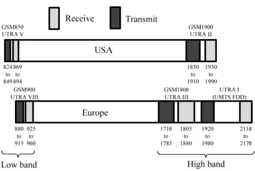
ACKGROUNDThe demand for compact internal WWAN (Wireless Wide Area Network) antenna which is embedded in the laptop computer covering penta-band operation is steadily growing [1]. This is a constant challenge for antenna designers, since higher degrees of global operation are sought, which, in turn, requires operation within continually more frequency. This is illustrated in Table I, which shows the nine bands allocated for the “3RD Generation”—or3G—UMTS Terrestrial Radio Access (UTRA) system. UTRA bands II, III, V, and VIII are also currently widely used by “2ND Generation”—or 2G—systems such as Global System for Mobile Communications (GSM). With the addition of UTRA band I, these bands allow quad-band 2G and tri-band 3G operation. Because of this, future laptop computer antennas are likely to be capable of operation in these bands, which are shown pictorially in Fig. 1.1 [2]. As indicated, bands II and V are used in the USA, whereas bands I, III, and VIII are used in Europe. All bands are also widely used worldwide, so designs of laptop computer antenna which covers the GSM850/900/1800/1900/UMTS operation frequency are required certainly.
TABLE I
UTRAFREQUENCY BANDS
Band TX(MHz) RX(MHz) I 1920-1980 2110-2170 II 1850-1910 1930-1990 III 1710-1785 1805-1880 IV 1710-1755 2110-2155 V 824-849 869-894 VI 830-840 875-885 VII 2500-2570 2620-2690 VIII 880-915 925-960 IX 1749.9-1784.9 1844.9-1879.9
Figure 1.1: Common cellular frequency bands used in Europe and the USA (MHz).
And with the tendency of reducing size of laptop computers, the space of integrated antennas is limited to the edge of laptop computer’s screen. When the conventional mobile communication antennas embedded in the laptop computers, it is difficult to achieve enough bandwidths or a larger antenna size is required for covering the penta-band operations. Therefore, by considering the thickness of laptop computers, printed antennas would be the proper radiating elements due to their low profile, small size and low weight, and their compatibility with planar surfaces. Furthermore, the width of antennas is mainly determined by the overall width of the edge of laptop computers, resulting in narrow and low profile needs. Nevertheless, when the antenna is very close to the ground plane, it is bound to be substantially eliminating current to reduce the antenna efficiency, thereby affecting the quality of communication.
In recent years achievements in improvement of the antennas’ operational characteristics, by the utilization of electromagnetic band-gap (EBG) structures [3-19], have been reported.The EBG surfaces have a periodic pattern, and specific properties would be obtained by properly designing their lattice periodicity. They can be considered as a new type of conducting surface which can suppress propagating surface
wave if properly designed, and unlike normal conductors, the surface impedance is large and the EBG performs as a magnetic conductor. Therefore, if an antenna is located close to the EBG surface, its currents and their images are in phase and the theoretically expected phase inverse of the field does not occur when it is scattered by a usual metallic surface. This property permits a current source to be located very close to the EBG surface, without the fields produced by this and its image current is canceled, whereas enhancement of antenna gain is obtained. Thus, the EBG can function as a unique new type of ground plane for low-profile antennas with high directive gain, efficiency, and bandwidth.
In summary, discovery of EBG structures has revealed promising solutions to the above problems. In this thesis, a new type 1-dimentional EBG structure will be proposed and used to high efficiency ground-proximity antenna designs. And the interaction of antennas and 1-D EBG structures are extensively investigated.
1.2
L
ITERATURES
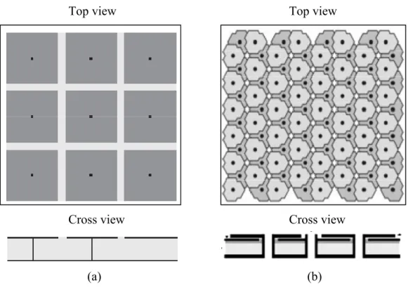
URVEYEBG structures are usually realized by periodic arrangement of dielectric materials and metallic conductors. In general, they can be categorized into three groups according to their geometric configuration: (1) three-dimensional volumetric structures, (2) two-dimensional planar surfaces.
Figure 1.2 shows two representative 3-D EBG structures: a mushroom-like structure [20] and woodpile structure consisting of patches [21]. Examples of 2-D EBG surfaces are plotted in Fig. 1.3: a uni-planar design without vertical vias [22] and a planar dual-band EBG structure [23].
Top view Top view
Cross view Cross view
(a) (b)
Figure 1.2: Three-dimensional EBG structures: (a) a mushroom-like structure and (b) a multi-layer metallic patch array.
Top view Top view
Cross view Cross view
(a) (b)
Figure 1.3: Two-dimensional EBG surfaces: (a) a uni-planar surface. (b) a dual-band EBG surfaces.
All of the mentioned EBG structures have similar operation characteristics, so we choose the most well known mushroom like 3-D EBG structure as an example, which is shown in Fig.1.2 (a). The structure consists of a periodic array of metal plates printed on a dielectric substrate, and each metal plate is connected to the ground plane using a
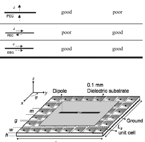
metal via. We defined L and C as the equivalent inductor and capacitor of a unit cell of the EBG structure, and the inductance of L depends on the thickness of the structure while the capacitance of C depends on the fringing electric fields between the pairs of metal plates. Thus the mushroom EBG structure forms a parallel LC circuit, and can be viewed as open circuit when this structure is operating at it’s resonance frequency.
This interesting feature have led to a wide range of applications in antenna engineering, from wire antennas to microstrip antennas, and from the conventional antenna structures to novel surface wave antenna concepts and reconfigurable antenna designs. An application of EBG is to design low profile wire antennas with good radiation efficiency, which is desired in modern wireless communication systems. To illustrate the fundamental principle, Table II compares the EBG with the traditional PEC ground plane in wire antenna designs. When an electric current is vertical to a PEC ground plane, the image current has the same direction and reinforces the radiation from the original current. Thus, this antenna has good radiation efficiency, but suffers from relative large antenna height due to the vertical placement of the current. To realize a low profile configuration, one may position a wire antenna horizontally close to the ground plane. However, the problem is the poor radiation efficiency because the opposite image current cancels the radiation from the original current. In contrast, the EBG surface is capable of providing a constructive image current within a certain frequency band, resulting in good radiation efficiency.
Based on this concept, various wire antennas have been constructed on the EBG ground plane [24, 25]. For example, Fig. 1.4 shows a printed dipole antenna on mushroom like EBG structures. By optimizing the interaction between the impedances of a primary and image dipoles with the reflection phase of an EBG structure, a wideband printed dipole antenna was designed. In summary, the EBG surface exhibits a great potential for low profile efficient wire antenna applications.
TABLE II
COMPARISONS OF CONVENTIONAL PECAND EBGGROUND PLANES IN WIRE ANTENNA DESIGNS
Options Efficiency Low profile
good poor
poor good
good good
Figure 1.4: Low profile dipole antenna over a finite EBG ground plane
However, the conventional EBG must be periodic, which represents a large area. And when designed with the antenna, it will become a 3-D structure which is too large for today's wireless communication applications, so conventional EBG structures are lack of practicality.
1.3
C
ONTRIBUTIONTo alleviate the above shortcomings of conventional EBG structures, this thesis presents a new type 1-D EBG structure, which both the antenna and EBG structure can be designed on the same plane to achieve an antenna in a limited narrow area in order to meet the needs of practical applications.
Fig. 1.5 shows the final design of printed ground-proximity monopole antenna with
plane for penta-band operation in the laptop computer. The antenna was designed with proposed 1-D EBG structures which are printed on the two sides of substrate respectively, the gray parts represent the metal on the top side, and the dotted rectangle represents the metal on the other side. All relevant parameters and designing steps of the proposed antenna will be discussed in Chapter 4.
Figure 1.5: A printed ground-proximity penta-band monopole antenna designed with 1-D EBG structures. (a) Top view. (b)Bottom view.
In the proposed antenna, two different 1-D EBG structures were used to achieve enough GSM bandwidth (824~960MHz), and these 1-D EBG structures also can be viewed as new radiators at high frequencies, thus composed a penta-band antenna. The ground plane size is 200mm × 300mm while the total size of antenna is 10mm × 63mm, which means the proposed antenna occupies a reasonable volume and is suitable to be employed in the narrow space between the top edge of the display panel and the casing of the laptop computer. In summary, the proposed 1-D EBG structure can achieve a series of design requirements, such as low profile, compact size, broad bandwidth, and multiple functionalities, and be used for nowadays commercial applications.
1.4
T
HESISO
RGANIZATIONThe thesis is organized as follows: Chapter 1 is an introduction, including the background, literature survey and contribution of proposed 1-D EBG structure. Chapter 2 presents the theory of EBG structures and shows the designing steps of the 1-D EBG structure. The simulation approaches and parameter investigations of the unit cell will also be shown in detail.
Chapter 3 depicts first application example of 1-D EBG structure, a high efficiency ground-proximity dipole antenna is proposed and used for GSM operation (824 MHz~ 960 MHz). The prototype is suitable to be embedded within a width of 10 mm between the top edges of the screen of a laptop and the antenna radiation efficiency is all above 55.6% in the using band.
Chapter 4 depicts a penta-band ground-proximity monopole antenna designed with 1-D EBG structures. Two different 1-D EBG structures are used in this antenna design to achieve enough GSM bandwidth. Also, the well designed 1-D EBG structures create new current paths at higher frequencies thus provide high bandwidth for
penta-band antenna. Furthermore, the total size of antenna is reduced and become more practical to commercial applications.
Finally, Chapter 5 concludes the overall thesis and also provides suggestions for the practical applications.
Chapter 2
E
LECTROMAGNETIC
B
AND
-G
AP
S
TRUCTURE
D
ESIGN
This chapter is devoted to the designing process of conventional EBG and proposed 1-D EBG structure. The first section will depict the theory of EBG structures, and the unit cell characteristics will be described in detail. The second section will illustrate simulation approaches of EBG structures and the EM simulated results of proposed 1-D EBG structure will be shown.
A 1-D EBG structure will be designed in the end of this chapter, which will be applied to the GSM antenna (824 MHz-960 MHz) in next chapter. Also, the EM simulation method illustrated in this chapter will be used to design different 1-D EBG structures in Chapter 4.
2.1 T
HEORY OFE
LECTROMAGNETICB
ANDG
AP(EBG)
S
TRUCTURES2.1.1 Theory of Conventional EBG Structure
When periodic structures interact with electromagnetic waves, characteristics such as frequency stop bands, pass bands, and band gaps could be identified. And periodic structures applications are seen in filter designs, gratings, frequency selective surfaces (FSS), photonic crystals and photonic band gaps (PBG), etc. We classify them under the broad terminology of “Electromagnetic Band Gap (EBG)” structures. Generally speaking, electromagnetic band gap structures are defined as artificial periodic (or sometimes non-periodic) objects that prevent/assist the propagation of electromagnetic waves in a specified band of frequency for all incident angles and all polarization states.
The EBG surfaces exhibit distinctive electromagnetic properties with respect to incident electromagnetic waves:
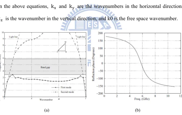
(1) When the incident wave is a surface wave (k k k , k is purely imaginary), the EBG structures show a frequency band gap through which the surface wave cannot propagate for any incident angles and polarization states. Atypical dispersion diagram is shown in Fig. 2.1(a).
(2) When the incident wave is a plane wave (k k k , k has a real value), the reflection phase of the EBG structures varies with frequency, as shown in Fig. 2.1(b). At a certain frequency the reflection phase is zero degrees, which resembles a perfect magnetic conductor that does not exist in nature.
In the above equations, k and k are the wavenumbers in the horizontal directions,
k is the wavenumber in the vertical direction, and k0 is the free space wavenumber.
(a) (b)
Figure 2.1: A planar EBG surface exhibits (a) a surface wave band gap and (b) an in-phase reflection coefficient for plane wave incidence.
Due to their unique band gap features, EBG structures can be regarded as a special type of metamaterial. Besides the band gap feature, EBG also possesses some other exciting properties, such as high impedance and PMC. For example, a mushroom-like EBG surface exhibits high surface impedances for both TE and TM polarizations. When
a plane wave illuminates the EBG surface, an in-phase reflection coefficient is obtained resembling an artificial magnetic conductor. These interesting features have led to a wide range of applications in antenna engineering.
2.1.2 Theory of 1-D EBG Structure
The unit cell of proposed 1-D EBG structure in shown in Fig.2.2 and is printed on the two sides of substrate respectively. The gray parts represent the metal on the top side, and the dotted rectangle represents the metal on bottom side, and both metals are connected by via. By considering the overlapping parts on the top and bottom sides, it can be seen as a parallel plate capacitor, which is circled by dotted line in Fig.2. And the current path through the via and the ground plane which is indicated by arrow line in Fig.2.2, provides an inductance. That is to say, when a plane waves transmits from + z axis towards –z axis, the equivalent circuit can be regarded as a parallel LC circuit. Both quantities form an equivalent parallel resonant circuit that describes the electromagnetic behavior of the material. Such structures perform as a high impedance surface around the specific frequency. Therefore, the metal ground plane can be regarded as PMC.
Figure 2.2: Unit cell of 1-D EBG structure. Dotted line circles parallel plate capacitor, and solid line elect current path through the via and the ground plane as an inductance.
Ground C L via z x
2.2 S
IMULATIONA
PPROACHES TOEBG
STRUCTURES2.2.1 Simulation for Conventional EBG Structure
To analyze unique features of EBG structures, various methods have been implemented. These methods can be put into three categories: (1) periodic transmission line method, (2) lumped element model, and (3) full wave numerical methods.
The periodic transmission line method is another popularly used technique to analyze EBG structures [26]. Fig. 2.3 depicts a transmission line model of EBG structures, where ZP is the impedance for each periodic element and XC is the coupling
capacitor. The Floquet periodic boundary condition is considered in this approach. After analyzing the cascaded transmission line, the dispersion curve can be readily obtained, which provides more information than the lumped element method. However, a difficulty in this method is how to accurately obtain the equivalent ZP and XC values for
the EBG structures. So this method won’t be used to design proposed 1-D EBG structure in this chapter.
Figure 2.4: Lumped LC model for EBG analysis
The lumped element model is the simplest one that describes the EBG structure as an LC resonant circuit [27], as shown in Fig. 2.4. The values of the inductance L and capacitance C are determined by the EBG geometry and its resonance behavior is used to explain the band gap feature of the EBG structure. This model is simple to understand, but the results are not very accurate because of the simplified approximation of L and C.
Owing to the fast development in computational electromagnetic, various numerical methods have been applied in the full wave simulations of EBG structures. .
The advantage of the full wave numerical methods is the versatility and accuracy in analyzing different EBG geometries. For example, Fig. 2.5 depicts a model for the mushroom-like EBG analysis [28], and shows a unit cell model for the computation of the reflection phase at normal incidence.
Figure 2.5: Full wave model of the EBG structure for reflection phase characterization.
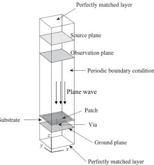
In Fig. 2.5, a single unit cell is surrounded by perfectly matched layers (PML) along the z direction, which are positioned 0.55 λ above the EBG to absorb the reflected energy. And surrounding periodic boundary conditions (PBC) in the horizontal directions is set to model an infinite periodic structure. Because it is impossible to directly simulate infinite structure using limited computation resources, the computation domain needs to be truncated using proper boundary conditions. For this purpose, a PBC that models the effect of periodic replication is introduced to truncate the computational domain so that only a single unit cell needs to be simulated. The normally incident plane wave is launched on the top source plane, and an observation plane is set to record the reflected phase from the EBG surface, and the height of the observation plane is 0.50 λ.
It is observed in Fig. 2.1(b) that the reflection phase of the EBG surface decreases continuously from 180◦ to −180◦ as frequency increases. At low-frequency and high-frequency regions, the EBG surface shows a similar phase to a PEC case, which is 180◦ (or−180◦). At the frequencies the EBG surface exhibits a reflection phase close to 0◦, it resembles a PMC surface.
2.2.2 Simulation for 1-D EBG Structure
As the paragraph we mentioned previously, EBG surfaces are usually characterized through the evolution of the reflection phase over the frequency. To assess its reflection behavior, the structure is exposed to a plane wave, and the phase of the incident and the reflected waves are compared. In these cases, a single unit cell is modeled, and through the use of Periodic Boundary Conditions (PBCs) this cell is repeated infinitely.
By using Ansoft High Frequency Structure Simulator (HFSS) full-wave simulation software [29], simulation settings show in Fig. 2.6(a) (b). Fig. 2.6(a) is vertical top view of using four 1-D EBG unit cells toward -x direction, Fig. 2.6(b) is the side view of
A-A' cross-plane. The top side of Fig. 2.6 (a) is port1, and the bold line represent PEC plane, dotted line represent PMC plane. Because of the boundary conditions of PEC planes, the metal structures mirror and the unit cells repeat infinitely on the PEC sides. Whereas the boundary conditions of PMC plane assure the TEM surface wave. These settings are designed to fulfill periodic structure and plane wave feeding. It is important that the simulated result of Fig. 2.6 is identical to the simulated result of one unit cell. The reason for setting four unit cells instead of one is to confirm that the asymmetric unit cell can also be repeated periodically and infinitely by this EM simulation setting.
(a)
(b)
Figure 2.6: The settings of 1-D EBG structure simulation: (a) top view (b) A-A’ side view.
PEC PEC PMC PMC E i E i y x L L ground x z E i PEC PEC A A’ E r port1 PEC
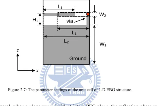
In next chapter, we will design a GSM (824MHz- 960MHz) antenna as an application of 1-D EBG structure, so we choose 880MHz as the center frequency of the EBG structure in this section. The designed parameters of the unit cell is shown in Fig.2.7, where L1 = 13.25 mm, L2= 19 mm, H1 = 4 mm, W1 = 10 mm, W2 = 1 mm, and
the used substrate is FR4 with relative dielectric constant 4.4 and thickness of 0.4mm.
Figure 2.7: The parameter settings of the unit cell of 1-D EBG structure.
In general, when a plane wave incident into a PEC plane, the reflection phase will theoretically be 180 °, and when a plane wave incident into a PMC plane, the reflection phase will be 0 °. Fig. 2.8 shows the phase of S11 and frequency response of the proposed 1-D EBG structure. At resonant frequency 880 MHz, the reflection phase of A-A’ plane equals to 0 °. This confirms that the structure is an EBG structure, thus can be regarded as a PMC plane.
The usable bandwidth of an EBG, when operating as a PMC plane, has been considered to be the frequencies over which the phase of the reflection coefficient is bounded by 90 degrees. The resonant frequency (fc) and fractional bandwidth (Fb) of 1-D EBG structure is given by formula (2.1) and (2.2):
Ground H1 via z x L1 L1 L2 W1 W2
√
(2.1)
(2.2)
It is well known that this in-phase reflection bandwidth for a parallel LC circuit is proportional to L/C, while the resonance frequency is proportional to√ 1/LC . Therefore, the in-phase reflection bandwidth increases due to the reduced C. And the increase in L for a specific resonance frequency has the added advantage of increasing bandwidth as smaller capacitance would be needed to achieve the same resonant frequency. Frequency (GHz) 0.6 0.7 0.8 0.9 1.0 1.1 1.2 Ph ase A ng le o f S 11 (d eg ) -180 -90 0 90 180
Figure 2.8: The reflection phase of 1-D EBG structure.
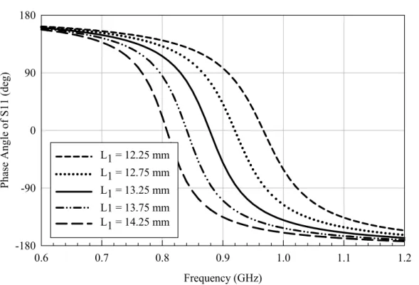
The resonant frequency of 1-D EBG structure can be designed by adjusting the length or width of the elements. Fig. 2.9 to Fig. 2.12 shows the changes in reflection phase while varying L1, H1, L2, and W2.
Fig. 2.9 shows that when L1 varies from 12.25 mm to 14.25 mm, the center
frequency moves from 970 MHz to 810 MHz and the bandwidth is decreasing. The resonant frequency is shifted downwards with increasing L1, since the increasing L1 will
increase coupling capacitance while it does not affect the value of inductance. The increasing coupling capacitor also reduces the bandwidth of 1-D EBG structure. Fig. 2.10 shows that when H1 varies from 3 mm to 5 mm, the center frequency moves from
938 MHz to 838 MHz and the bandwidth is increasing. The resonant frequency is also shifted downwards with increasing H1, since the longer H1 contributes to larger
inductance while it does not affect the value of coupling capacitance. The lager inductance causes larger bandwidth, but also need more designing space. Fig. 2.11 shows that when L2 varies from 17 mm to 21 mm, the center frequency moves from 860
MHz to 925 MHz and the bandwidth is increasing .The resonant frequency is shifted upwards with increasing L2, since the increasing L2 contributes to increasing value of
inductance and decreasing value of coupling capacitance. Although longer L2 will
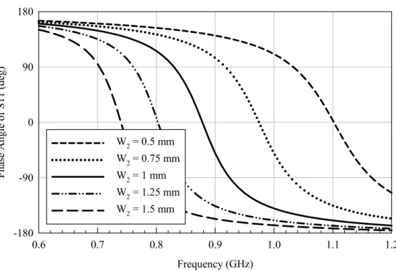
increase the unit cell size, the bandwidth of 1-D EBG can be improved effectively. Fig. 2.12 shows that when W2 varies from 0.5 mm to 1.5 mm, the center frequency moves
from 1100 MHz to 740 MHz and the bandwidth is decreasing. The resonant frequency is shifted downwards with increasing W2. The increasing W2 contributes to the
increasing coupling capacitance while it does not affect the value of inductance. Also, lager coupling capacitance causes smaller bandwidth of 1-D EBG structure.
This simulation method yields good results when studying the theoretical behavior of the 1-D EBG surface, but does not assess real situations, in which the structure is always finite in size. For example, the characteristic properties of antennas are strongly influenced by the size of the ground plane, so it is therefore important to determine how the truncation of the infinite EBG cell distribution will affect the performance. The antenna applications of 1-D EBG structure will be proposed in Chapter 3 and Chapter 4.
Frequency (GHz) 0.6 0.7 0.8 0.9 1.0 1.1 1.2 Ph ase A ng le o f S 11 (d eg) -180 -90 0 90 180 L1 = 12.25 mm L1 = 12.75 mm L1 = 13.25 mm L1 = 13.75 mm L1 = 14.25 mm Figure 2.9: The reflection phase of 1-D EBG structure with H1 = 4mm, L2 = 19mm, W2=1mm and
varied L1 from 12.25 mm to 14.25 mm. Frequency (GHz) 0.6 0.7 0.8 0.9 1.0 1.1 1.2 P hase An gle o f S 11 ( deg ) -180 -90 0 90 180 H1 = 3 mm H1 = 3.5 mm H1 = 4 mm H1 = 4.5 mm H1 = 5 mm
Figure 2.10: The reflection phase of 1-D EBG structure with L1 = 13.25mm, L2 = 19mm, W2=1mm and varied H1 from 3 mm to 5 mm..
Frequency (GHz) 0.6 0.7 0.8 0.9 1.0 1.1 1.2 P ha se An gle of S1 1 (deg) -180 -90 0 90 180 L2 = 17 mm L2 = 18 mm L2 = 19 mm L2 = 20 mm L2 = 21 mm
Figure 2.11: The reflection phase of 1-D EBG structure with H1 = 4mm, L1 = 13.25mm, W2=1mm and varied L2 from 17 mm to 21 mm.
Frequency (GHz) 0.6 0.7 0.8 0.9 1.0 1.1 1.2 Ph as e An gl e of S11 (deg) -180 -90 0 90 180 W2 = 0.5 mm W2 = 0.75 mm W2 = 1 mm W2 = 1.25 mm W2 = 1.5 mm
Figure 2.12: The reflection phase of 1-D EBG structure with H1 = 4mm, L1 = 13.25mm, L2=19mm and varied W2 from 0.5 mm to 1.5 mm.
Chapter 3 A
H
IGH
E
FFICIENCY
G
ROUND
-P
ROXIMITY
D
IPOLE
A
NTENNA
The 1-D EBG structure has been characterized and designed in previous chapter, and now we shift our focus to 1-D EBG applications in antenna engineering. The important property of 1-D EBG structures is the phase response to the plane wave illumination, where the reflection phase changes from 180◦ to −180◦ as the frequency increases. In this chapter, we utilize this property to improve the radiation efficiency of a dipole antenna near a ground plane.
The proposed antenna is shown in Fig. 3.1, we applied the 1-D EBG structure to the ground-proximity dipole antenna, thus the impedance matching and antenna gain degrade problem can be improved. Hence, the dipole antenna can be placed close to the high impedance surface of 1-D EBG structure on the ground plane and maintained the antenna performance. The used 1-D EBG structure will be shown briefly in section 3.1, design considerations of the dipole antenna with 1-D EBG structure are described in section 3.2, and measured results are presented in section 3.3.
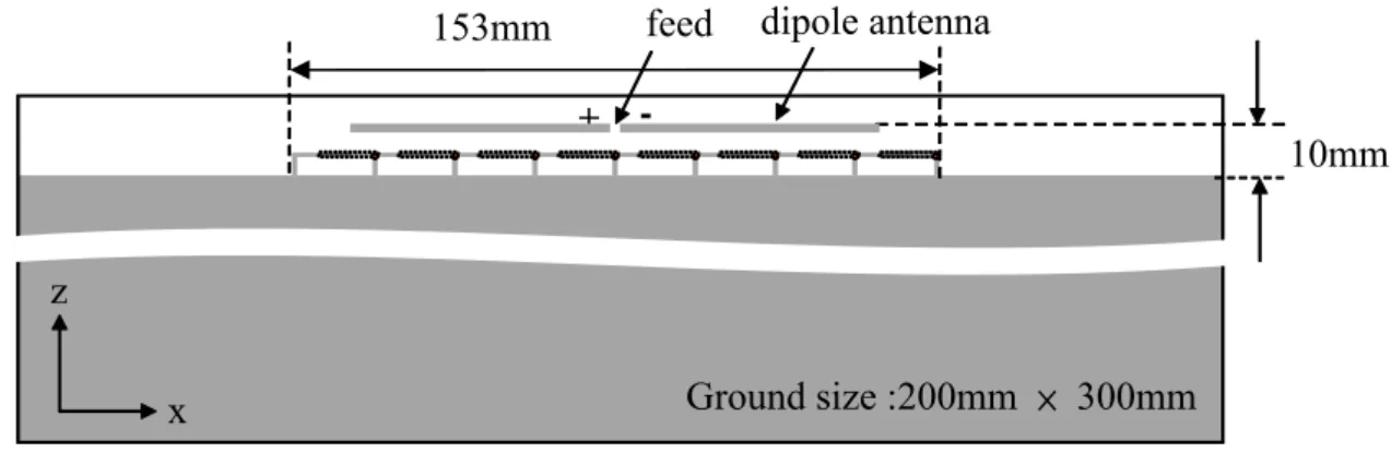
Figure 3.1: A high efficiency ground-proximity dipole antenna designed using 1-D EBG structure, and the total size of antenna is 10 mm 153 mm.
153mm
10mm
Ground size :200mm × 300mm feed dipole antenna
+
-x z
3.1
D
ESIGN OF1-D
EBG
S
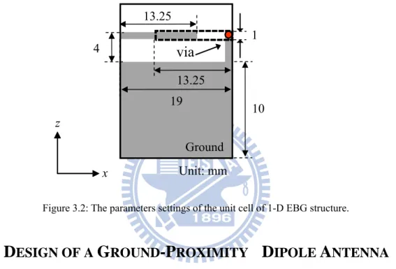
TRUCTUREIn this chapter, we use the 1-D EBG structure which was proposed in Chapter 2 and the unit cell parameters is shown in Fig. 3.2. The used substrate is FR4 with relative dielectric constant 4.4 and thickness of 0.4mm and the center frequency of this 1-D EBG structure is 880MHz.
Figure 3.2: The parameters settings of the unit cell of 1-D EBG structure.
3.2
D
ESIGN OF AG
ROUND-P
ROXIMITYD
IPOLEA
NTENNAFig.3.1 is an application of 1-D EBG structure used in planar antenna design with a typical dipole antenna. We placed a designed dipole antenna next to the ground with 1-D EBG structure. The proposed antenna was designed for laptop computer application, so the ground size is 200 mm × 300 mm, which is used to simulate the upper ground plane of laptop computer.
The antenna is printed on the two sides of substrate respectively, the gray parts represent the metal on the top side, and the dotted rectangle represents the metal on the other side, and both metals of 1-D EBG structures are connected by via. Fig. 3.3 shows the related parameters of the antenna, where L1 = 13.25 mm, L2 = 19 mm, L3 = 61 mm,
Ground 4 z x 13.25 13.25 19 10 Unit: mm 1
via
H1 = 4 mm, H2 = 10 mm. The length of dipole is used to tune the impedance match of
the antenna. Therefore, the length of the dipole is not necessarily half-wavelength, and the simulated results show that a proper length is around 0.65λ for the proposed dipole antenna. Consequently, the total size of the proposed antenna is 10 mm 153 mm.
Ground size: 200mm × 300mm L3 L1 H1 feed +_ L2 L1 H2 x z
dipole antenna 1-D EBG unit cell
Figure 3.3: Parameters of the proposed antenna.
When the dipole antenna placed too close to a ground plane, the mirror current generated by the dipole antenna on the ground will be opposite to the current on the dipole antenna, which canceled each other. So both the impedance matching and radiation of the dipole antenna are destructed. However, when the edge of the ground added 1-D EBG structure, although the dipole antenna is very close to the ground plane, the antenna will still be able to maintain its original characteristics. This is because when a dipole is positioned on an EBG ground plane, no surface wave can be excited because of the surface wave band gap of the 1-D EBG structure. This phenomenon can be observed in current distribution diagram, which is shown in Fig. 3.4. The current distribution along the ground plane is weak at the resonance frequency of used 1-D EBG structure, that means the image current of the dipole antenna was suppressed by the 1-D EBG structure and the dipole antenna can radiate without being affected.
Figure 3.4: Current distributions of the dipole antenna with 1-D EBG structure at 880 MHz.
Fig. 3.5 shows the simulation results of return loss for original dipole antenna, dipole antenna with ground, and dipole antenna with 1-D EBG structure. In Fig. 3.5, the resonant frequencies are different between original dipole antenna and the dipole antenna with 1-D EBG structure. This is because when 1-D EBG structure was added, the far right and left unit cells of 1-D EBG structure will lead the equivalent length of antenna longer, and then cause the lower resonant frequency. Fig. 3.5 shows dipole antenna with 1-D EBG structure can achieve GSM bandwidth (824MHz~960MHz) ranges from 820MHz to 982MHz with a reflectivity of less than -6 dB.
Figure 3.5: The simulated return loss of dipole antenna, dipole antenna with ground, and dipole antenna with 1D-EBG structure.
Frequency (GHz) 0.6 0.7 0.8 0.9 1 1.1 1.2 15 10 5 0 Ret urn Lo ss (d B) 20
Dipole with 1-D EBG Dipole
3.3
E
XPERIMENTALR
ESULTSThe realized proposed antenna is shown in Fig. 3.6.
(a)
(b)
Figure 3.6: Photograph of the fabrication for the proposed antenna. (a) Top view. (b) Bottom view.
Zoom in photo for antenna:
Ground size: 200mm × 300mm Zoom in photo for antenna:
In Fig. 3.7, the dotted line represents the measured result and solid line represents the simulated result of dipole antenna with 1-D EBG structure. The measured bandwidth ranges from 802MHz to 968MHz with a reflectivity less than −6 dB, and the simulated and measured results come to a great agreement.
Figure 3.7: Simulated and measured results of dipole antenna with 1D-EBG structure.
Fig. 3.8 (b) depicts the measured and simulated radiation pattern of dipole antenna with ground in yz plane. In general, the radiation pattern of dipole antenna in this plane should be omnidirectional. However, the short distance between antenna and ground plane cause the mirror current on the ground plane opposite to the current on the antenna, and thus eliminate each other. This leads to skew radiation pattern. Fig. 3.8(a) is the measured and simulated radiation patterns of dipole antenna with 1-D EBG structure in yz plane. Compared Fig. 3.8 (a) to Fig. 3.8 (b), the radiation pattern becomes more identical to the radiation pattern of theoretical dipole antenna after adding 1-D EBG structure. This is because the mirror current on the ground is no longer reversed-phase when 1-D EBG structure is added. Therefore, 1-D EBG structure is able to improve the skewed pattern of the original problem.
Frequency (GHz) 0.8 0.9 1 Measurement Simulation 0.95 0.85 25 15 10 5 0 Ret urn L oss (dB) 20
Figure 3.8: Radiation patterns in yz plane of (a) dipole antenna with 1-D EBG structure. (b) Dipole antenna with ground..
In the design of traditional antennas which work in free space, the measured parameters are often the reflection coefficient S11 and the radiation patterns measured in the E or H planes around the antenna. The reflection coefficient describes how much of the available power is reflected at the antenna port, but it does not give any information about whether the remainder of the power is radiated or dissipated in the antenna. Therefore, the reflection coefficient alone cannot determine if the antenna is a good or a poor radiator. The efficiency is defined as being the total radiated power divided by the maximum available power when the antenna is impedance matched. The antenna efficiency includes the effects of mismatch, as well as absorption in the antenna and it’s near field environment such as 1-D EBG structure.
As 1-D EBG structure absorbing part of the energy radiated from the antenna, efficiency becomes the key factor in the antenna design. Usually stronger ground current leads to higher energy losses, and moreover, less separation between them introduces stronger coupling effects. It is the in-phase reflection feature given by 1-D
-35-30-25-20-15-10 -5 0 5 -35 -30 -25 -20 -15 -10 -5 0 5 0 30 60 90 120 150 180 210 240 270 300 330 Measurement Simulation -35-30-25-20-15-10 -5 0 5 -35 -30 -25 -20 -15 -10 -5 0 5 0 30 60 90 120 150 180 210 240 270 300 330 Measurement Simulation
EBG structure that effectively decreases the energy absorbed by the ground, thus improving the antenna efficiency.
Fig. 3.9 indicates the antenna efficiency in the given conditions: dipole antenna with ground and dipole antenna with 1-D EBG structure. As illustrated in those results, the dipole antenna with 1-D EBG structure has peak antenna efficiency 81.7% at 860MHz, when the dipole antenna is placed close to the ground without 1-D EBG structure, the antenna efficiency peak drops to 50.4% at 920MHz. In the bandwidth of GSM (824 MHz -960 MHz), the antenna efficiency of the dipole antenna with 1-D EBG structure are all above 55.6%, which has at least 10% enhancement to the case without 1-D EBG structure. Frequency (GHz) 0.80 0.85 0.90 0.95 1.00 A nten na Ef ficien cy( % ) 0 20 40 60 80 100
Dipole with 1-D EBG
Dipole without 1-D EBG with ground
Figure 3.9: Antenna efficiency of dipole antenna with ground and dipole antenna with 1-D EBG structure.
Chapter 4 A
P
ENTA
-
BAND
G
ROUND
-P
ROXIMITY
M
ONOPOLE
A
NTENNA
In the previous chapter, a ground-proximity dipole antenna was proposed and the efficiency in GSM band has at least a 10% improvement by adding 1-D EBG structure. So we have confirmed that the 1-D EBG structure can shorten the necessary distance between antenna and ground plane, and allows antennas to maintain the original radiation characteristics. However, the total size of the dipole antenna proposed in
Chapter 3 (10 mm 153 mm) is still too large for commercial applications. Also the
bandwidth only covers GSM band, which is not enough for WWAN antennas. Therefore, a more compact antenna with wider bandwidth is certainly demanded.
In this chapter, a penta-band ground-proximity monopole antenna is designed for laptop computer applications. Two 1-D EBG structures are applied to achieve low bandwidth while the structures can radiate in high band. In section 4.1, all design considerations and simulations of two new 1-D EBG structures will be illustrated. Those two 1-D EBG structures will be applied to ground-proximity monopole antennas respectively in section 4.2. Because either of the antenna does not have enough bandwidth for GSM operation, we combine those two 1-D EBG structures together in section 4.3. Furthermore, we adjusted part of the 1-D EBG structures slightly for impedance matching and create resonance at high frequencies, thus achieve penta-band requirement. And in the end of the section, an additional size reduction design will be proposed. The final design of the penta-band monopole antenna with proximate ground
plane is shown in Fig. 4.1, and the total size of proposed antenna is 10 mm 63 mm,
which is more compact and applicable than the dipole antenna proposed in Chapter 3. The measured results are presented in section 4.4.
Figure 4.1: A printed penta-band ground-proximity monopole antenna designed using 1-D EBG structures. (a) Top view. (b) Bottom view.
4.1 D
ESIGN OF1-D
EBG
S
TRUCTURESTwo different 1- EBG structures are proposed in this section. The parameters of first 1-D EBG structure is shown in Fig.4.2, which is similar to the proposed structure in Chapter 3. This 1-D EBG structure can be viewed as parallel LC, and it is well known that the in-phase reflection bandwidth for a parallel LC circuit is proportional to L/C, while the resonance frequency is proportional to√ 1/LC . So for certain resonance frequency, we fixed the total capacitance and inductance of the 1-D EBG structure, which means we varied L2 and L3 together with fixed H2, L4 and L2 + L3. Fig. 4.3 shows
L3 =18 mm with fixed L4 = 25 mm and H2=4.6 mm. The different combinations of L2
and L3 would be useful for impedance matching when we applied the 1-D EBG
structure to antennas. The optimized parameters are L2 = 14.5 mm, L3= 18 mm, L4= 25
mm, H2 = 4.6 mm, W3 = 1 mm, and the designed resonance frequency of first 1-D EBG
structure is 840 MHz.
Figure 4.2: The unit cell of first 1-D EBG structure.
Frequency (GHz) 0.6 0.7 0.8 0.9 1.0 1.1 1.2 P has e A ngle of S 11 ( deg) -180 -90 0 90 180 L2 = L3 = 16.25 mm L2 = 14.5 mm, L3 =18 mm
Figure 4.3: The reflection phase of first 1-D EBG structure with fixed L4 = 25 mm and H2= 4.6 mm.
Ground H2 z x L3 L4
via
W3 L2The second 1-D EBG structure is shown in Fig. 4.5. The Fig. 4.5(a) depicts that the metal on the top right side of the unit cell can be viewed as a small monopole, which is equivalent to a shunt inductor (L). The microstrip line on the bottom left side couples to ground and forms a capacitor (Cground). And the overlapping parts on the top and bottom sides can be seen as a parallel plate capacitor (Ccoupling). In summary, the equivalent circuit of the structure is also a parallel LC circuit, which can form a 1-D EBG structure. The advantage of this 1-D EBG structure is easier to fabricate without using vias. Furthermore, it can be viewed as a monopole antenna at higher frequency if the impedance is matched well. However, more space is needed in this structure, because the second 1-D EBG structure needs longer microstrip line to achieve enough inductance without vias.
The optimized parameters of second 1-D EBG structure are illustrated in Fig 4.5(b), where L5 = 22 mm, L6= 14 mm, L7= 30 mm, H3 = 7.8 mm, W3 = 1 mm, and the
designed resonance frequency is 950 MHz.
(a) (b) Figure 4.4: The unit cell of second 1-D EBG structure.
(a) The equivalent circuit. (b) The parameters setting.
Ground H3 z x L5 L6 L7 W3 W4 Ground z x Cground Ccoupling L
The reflection phase of the second 1-D EBG structure is shown in Fig 4.5. We can notice that the bandwidth of this structure is wider than the first one because of
comparatively larger inductance and smaller capacitance.
Frequency (GHz) 0.6 0.7 0.8 0.9 1.0 1.1 1.2 P has e A ng le o f S 11 ( de g) -180 -90 0 90 180
Figure 4.5: The reflection phase of second 1-D EBG structure.
4.2 D
ESIGN OFG
ROUND-P
ROXIMITYM
ONOPOLEA
NTENNASNow we apply two proposed 1-D structures to monopole antennas respectively. We place a designed monopole antenna next to four unit cells of 1-D EBG structure on a 200mm × 300 mm ground plane, which is shown in Fig. 4.6 and Fig. 4.7. The monopole antenna is made of a 1.8 mm microstrip line and located on the center of the ground plane. To maintain the low profile advantage, the width of the monopole antenna is set to 10 mm. The physical parameters of the designed monopole antennas according to Fig. 4.6 and Fig. 4.7 are listed in Table III.
L1' W1 W3 L4 L2 W2 H2 H1 feed + _ x z via Ground size: 200mm × 300mm (a)
Figure 4.6: A monopole antenna designed with first 1-D EBG structure. (a) Top view. (b) Bottom view.
Figure 4.7: A monopole antenna designed with second 1-D EBG structure. (a) Top view. (b) Bottom view.
TABLE III
THE PARAMETERS OF THE MONOPOLE ANTENNAS DESIGNED WITH 1-DEBG
STRUCTURES IN FIG.4.6AND FIG 4.7
Parameters H1 H2 H3 L1’ L1” L2 L3 L4 L5 L6 L7 W1 W2 W3 W4 Unit:mm 10 4.6 7.8 52 48 14.5 18 25 22 14 30 10 1.8 1 2
The position that we placed 1-D EBG structure will both affect the impedance matching and the current path on the monopole antenna, so we vary the distance between feed point and the 1-D EBG structures to optimize performance of the antenna. And the lengths of the monopole antennas are also designed different slightly according to the different 1-D EBG structure for impedance matching.
This effect of 1-D EBG structures can be observed in current distribution diagram, which is shown in Fig. 4.8. The current distribution along the ground plane is weak at the resonance frequency of the applied 1-D EBG structure (840 MHz or 950 MHz). That means the image current of the monopole antenna on the ground was suppressed by 1-D EBG structure, thus the monopole antenna can radiate without being affected.
(a)
(b)
Figure 4.8: Current distributions of the proposed monopole antennas. (a) The monopole antenna with first 1-D EBG structure at 840 MHz. (b) The monopole antenna with second 1-D EBG structure at 950 MHz.
Moreover, most of the energy is bounded in the first two unit cells of the right side, which are the nearest to the feed point of monopole antennas. Therefore, we conclude that these two unit cells dominate the performance of 1-D EBG structure while the others are not necessary. So we can reduce the required number of unit cells and achieve a more compact antenna design. This miniaturized method will be used in next section, and the size of antenna can be reduced approximately 50 percent.
The simulated return loss of proposed monopole antennas are shown in Fig 4.9. The bandwidth of first monopole antenna is 810 MHz to 880 MHz, and the other is 911 MHz to 995 MHz. The simulated result confirms that the second 1-D EBG structure provides wider bandwidth as we mentioned in previous section. However, neither of the antenna have enough bandwidth for GSM, so these two 1-D EBG structures need to be combined to achieve wider bandwidth in next section.
Frequency(GHz) 0.6 0.7 0.8 0.9 1.0 1.1 1.2 R eturn l oss( dB ) 0 5 10 15 20 25 Monopole antenna with first 1-D EBG Monopole antenna with second 1-D EBG
Figure 4.9: The simulated return loss of a monopole antenna with first 1D-EBG structure and a monopole antenna with second 1D-EBG structure.
4.3 D
ESIGN OF AP
ENTA-
BANDG
ROUND-P
ROXIMITYM
ONOPOLEA
NTENNAIn this section, the shortcomings mentioned in the previous section will be improved. A compact penta-band monopole antenna designed using two different kinds of 1-D EBG structures is proposed and shown in Fig. 4.10. We combined these two 1-D EBG structures together to achieve wider bandwidth in low band (824 MHz - 960 MHz), and only two unit cells of each 1-D EBG structures are used to miniaturize the total size
of antenna. The total size of proposed antenna is 10 mm 63 mm, which is applicable
to laptop computers. The parameters of the designed monopole antenna according to Fig. 4.10 are listed in Table IV.
TABLE IV
THE PARAMETERS OF PROPOSED PENTA-BAND MONOPOLE ANTENNA
Parameters H1 H2 H3 L1 L2 L3 L4 L5 L6 L7 W1 W2 W3 W4 W5 Unit:mm 10 4.6 7.8 51 14.5 18 25 22 14 30 10 1.8 1 2 5.8
Figure 4.11 presents the simulated return loss results of the proposed antenna. A monopole antenna with a ground plane is also simulated as a reference. When the monopole antenna is placed near to a ground plane, the radiation from the reverse image current cancels the radiation from the original monopole antenna. Thus, the return loss is only above −5.8 dB. When those two 1-D EBG structures are applied together, the return loss improves significantly. A GSM bandwidth (824 MHz - 960 MHz) is achieved in this design, and the low bandwidth ranges from 820 MHz to 1120 MHz. Furthermore, the 1-D EBG structures also radiate in high band (1710 MHz – 2170MHz), thus a penta-band antenna can be achieved after additional impedance matching.
Frequency(GHz) 0.6 0.8 1.0 1.2 1.4 1.6 1.8 2.0 2.2 Retur n los s( dB) 0 5 10 15 20 25 Monopole antenna with 1-D EBG structures
Monopole antenna with ground
Figure 4.11: The simulated return loss of proposed penta-band monopole antenna with 1-D EBG structures, and monopole antenna with ground.
The length of monopole antenna (L1) is slightly different to the previous
applications in Fig. 4.6 and Fig 4.7. To design proper length of monopole antenna, the parameters of the 1-D EBG structures are kept the same while the monopole length is changed during the simulations. Thus, the monopole antenna will resonate at different frequencies. Since the electromagnetic property of the 1-D EBG structures are a function of frequency, its interaction with the monopole antenna is also frequency dependent. As a result, the radiation efficiency of the monopole antenna will vary with frequency. In the operational frequency band where the 1-D EBG structures provide a constructive interaction, the monopole antenna can achieve a good return loss and radiation patterns. Therefore, by observing the return loss value and radiation patterns of the monopole at different frequencies, one can find the useful operational frequency band of the 1-D EBG structures.
After combining two 1-D EBG structures, the characteristics of both structures may change unexpectedly. Therefore, we discuss the structures respectively to observe the performance of 1-D EBG structures. First, the current distribution diagram is shown in Fig. 4.12 at the resonance frequency of first 1-D EBG structure (840 MHz). Compared to Fig. 4.8(a), the current distribution is almost the same, which means the characteristics of first 1-D EBG structure remain the same at 840 MHz.
Second, the current distribution diagram is shown in Fig. 4.13(a) at the resonance frequency of second 1-D EBG structure (950 MHz). Compared to Fig. 4.8(b), the current distribution is almost the same, which means the characteristics of second 1-D EBG structure remain the same at 950MHz. Furthermore, the unit cells of second 1-D EBG structure can radiate individually in high band. To achieve enough high bandwidth, one of the unit cells of second 1-D EBG structure is modified. Because of the difference between W4 and W5, unequal resonance frequencies in high band are created (1.8 GHz
and 2.05 GHz) while the characteristics of second 1-D EBG structure in low band maintain the same. This phenomenon can be observed in current distribution diagram in Fig. 4.13. Fig. 4.13 (b) and (c) show the current distribution in high bands, which are dominated by the length and height of second 1-D EBG structure on the top side (L5 and
H3). The resonance frequency of the left unit cell, where the strong current distribution
is shown in Fig. 4.13 (b), is 1.8GHz. And the resonance frequency of the right unit cell, where the strong current distribution is shown in Fig. 4.13 (c), is 2.05GHz. The simulated return loss shown in Fig. 4.14 helps to demonstrate this property. It shows that the center frequency moves from 1.05 GHz to 1.15 GHz in low band as L5 changes
from 23 mm to 21 mm. As expected, the lowest resonance almost remains the same since the first 1-D EBG structure was not changed. The resonances in high band are both decreasing with increasing L5, since the resonances are created by the second 1-D
EBG structure in high band. Thus we can conclude that those two unit cells of second 1-D EBG can be designed to achieve the bandwidth from 1.7 GHz to 2.2 GHz, which covers the high band of penta-band application.
(a)
(b)
(c)
Figure 4.13: Current distributions of the proposed penta-band monopole antenna at (a) 0.95 GHz (b) 1.8 GHz (c) 2.05 GHz. Frequency (GHz) 0.6 0.8 1.0 1.2 1.4 1.6 1.8 2.0 2.2 Re tur n loss( dB ) 0 5 10 15 20 25 L5 = 23 mm L5 = 22 mm L5 = 21 mm
4.4 E
XPERIMENTALR
ESULTSThe realized proposed antenna is shown in Fig.4.15.
(a)
(b)
Figure 4.15: The realized proposed antenna. (a) Top view. (b) Bottom view.
Ground size: 200mm × 300mm Zoom in photo for antenna:
Zoom in photo for antenna:
In Fig. 4.16, the solid line represents the measured result and dotted line represents the simulated result of the proposed penta-band monopole antenna with 1-D EBG structures. The measured bandwidth ranges from 820 MHz to 1103 MHz and 1708 MHz to 2190 MHz with a reflectivity less than −6 dB. The measured and simulated results are generally identical, while the performance from 1900 MHz to 2100 MHz is poorer when measurement. Although the measurement is not as ideal as simulation, the bandwidth is still enough for penta-band application.
Frequency(GHz) 0.6 0.8 1.0 1.2 1.4 1.6 1.8 2.0 2.2 Ret u rn l o ss( dB) 0 5 10 15 20 Measurement Simulation
Figure 4.16: Simulated and measured results of proposed penta-band monopole antenna.
To illustrate the effect of 1-D EBG structures, we simulated and measured the radiation patterns of monopole antennas in two configurations: the proposed monopole antenna with 1-D EBG structures and a monopole antenna with ground plane. The antenna patterns are measured and simulated at 890 MHz and the xz, yz, and xy plane patterns are sketched in Fig. 4.17. The short distance between antenna and ground plane cause the mirror current on the ground plane opposite to the current on the antenna, and
thus eliminate each other, which leads to skew radiation pattern. By comparing the radiation pattern between the monopole antenna with and without 1-D EBG structures, the radiation pattern become more identical to theoretical radiation pattern of monopole antenna after adding 1-D EBG structures. It can be inferred from Fig. 4.17 that the radiation power is nearly omni-directional, so 1-D EBG structure is able to improve the skewed pattern of the original problem.
Phi = 0° Phi = 90°
Theta = 90°
Figure 4.17: The measured and simulated patterns of monopole antenna with 1-D EBG structures and monopole antenna with ground at 890MHz.
-35 -30 -25 -20 -15 -10 -5 0 5 -35 -30 -25 -20 -15 -10 -5 0 5 0 30 60 90 120 150 180 210 240 270 300 330 -35 -30 -25 -20 -15 -10 -5 0 5 -35 -30 -25 -20 -15 -10 -5 0 5 0 30 60 90 120 150 180 210 240 270 300 330 -35 -30 -25 -20 -15 -10 -5 0 5 -35 -30 -25 -20 -15 -10 -5 0 5 0 30 60 90 120 150 180 210 240 270 300 330
phi=0 830 sim vs Col 1 phi=0 830 me vs Col 1 monopole antenna vs Col 1 SIM vs Col 1
Measurement of monopole antenna with 1-D EBG structures
Simulation of monopole antenna with 1-D EBG structures
Measurement of monopole antenna with ground plane
Simulation of monopole antenna with ground plane
And the xz, yz, and xy plane antenna patterns are measured at 1750 MHz, 1900 MHz, and 2150MHz in Fig.4.18 and Fig.4.19. The total radiation pattern is contributed to the direct radiation from the proposed monopole antenna and the radiation power is almost omni-directional In addition to–z direction. It is interesting to notice that the lobes on –z direction are significantly lower because of the large PEC plane placed on –z direction.
Phi = 0° Phi = 90°
Theta = 90°
Figure 4.18: The measured and simulated patterns of proposed penta-band monopole antenna at 1750MHz. -35 -30 -25 -20 -15 -10 -5 0 5 -35 -30 -25 -20 -15 -10 -5 0 5 0 30 60 90 120 150 180 210 240 270 300 330 Measurement Simulation -35 -30 -25 -20 -15 -10 -5 0 5 -35 -30 -25 -20 -15 -10 -5 0 5 0 30 60 90 120 150 180 210 240 270 300 330 Measurement Simulation -35 -30 -25 -20 -15 -10 -5 0 5 -35 -30 -25 -20 -15 -10 -5 0 5 0 30 60 90 120 150 180 210 240 270 300 330 Measurement Simulation