國
立
交
通
大
學
電子工程學系 電子研究所碩士班
碩
士
論
文
具複雜運算單元之低功率多執行緒資料路徑
的研究與設計
Study on Improving Utilization for Low-Power
Multithreaded Datapath with Composite
Functional Units
研究生: 卓毅
指導教授: 劉志尉 博士
具複雜運算單元之低功率多執行緒資料路徑的研究與設計
Study on Improving Utilization for Low-Power Multithreaded Datapath
with Composite Functional Units
研 究 生:卓毅
Student: Yi Cho指導教授:劉志尉 博士
Advisor: Dr. Chih-Wei Liu國 立 交 通 大 學
電子工程學系 電子研究所碩士班
碩士論文
A Thesis
Submitted to Department of Electronics Engineering & Institute of Electronics College of Electrical Engineering and Computer Science
National Chiao Tung University in partial Fulfillment of the Requirements
for the Degree of Master of Science
in
Electronics Engineering
October 2007
Hsinchu, Taiwan, Republic of China
具複雜運算單元之低功率多執行緒資料路徑
的研究與設計
研究生:卓 毅
指導教授:劉志尉 博士
國立交通大學
電子工程學系 電子研究所
摘要
在觀察近年來處理器的發展演變中我們發現,簡化指令集處理器(RISC)已 成為一大設計主流。其簡單和規律的指令集設計很容易進一步的將指令執行管線 化(pipeline)提高處理器效能。然而,因為分派一個指令,只能執行一個動作導致 其硬體使用率不高。多指令分發(multi-issue)處理器,即超長指令(VLIW)處理器, 利用指令層級平行度(ILP)提高硬體使用率,但它的暫存器檔案面積,隨著運算 單元增加而劇烈成長,因而付出沉重的硬體代價。在本論文中,我們提出一個具 複雜運算單元(composite FU)的資料路徑,以客製化順序串接多個運算單元的方 式,在同一指令中處理連續多個基本運算(primitive operations),達到硬體使用率 的提升。此複雜運算單元不僅可以減輕如VLIW 的暫存器面積會因功能單元(FU) 增加而大幅成長的問題,還因為複雜運算單元可以在抓取運算子後,作多個運算 才存回,總暫存器存取次數得到節省,進而得到低功率的好處。此外我們也利用 整合管線化設計 流程 來提升整體效能(操作頻率),以及搭配交錯多執行緒 (interleaved multithreaded)架構來完全地隱藏管線化後所衍生的指令延遲。我們同 時提出一個自動化複雜運算單元產生器,藉由分析使用者所輸入的應用程式資料 流程圖(data-flow graph),自動產生出一個最佳化的複雜運算單元。經由對多個典 型DSP 應用分析,複雜運算單元 MSA(串接一個乘法器 M 以及一個移位器 S 和加法器A)的硬體使用率(operation per cycle)和簡化指令集處理器的 1.00 比較提升
為1.35。使用台積電 0.13um 製程作合成分析,在同樣的運算效能下,複雜運算
單元較簡化指令集合的面積約多 10%,但較超長指令減少約 50%。複雜運算單
Study on Improving Utilization for Low-Power
Multithreaded Datapath with Composite
Functional Units
Student: Yi Cho Advisor: Dr. Chih-Wei Liu
Department of Electronics Engineering Institute of Electronics
National Chiao Tung University
ABSTRACT
From the observation of evolution of processor development in recent years, we find that Reduced Instruction Set Computer (RISC) processors have already become main design fashion. The simplicity and regularity of RISC is suitable for pipeline design to boost performance. However, its hardware utilization is low because of it execute only one operation in single instruction issued. Multi-issue (VLIW) processors, takes advantage of the Instruction Level Parallelism (ILP) to promote hardware utilization. But the register file (RF) area of VLIW grows exaggeratedly with the increase of the functional unit number. It pays a great hardware overhead. In this thesis, we propose a datapath with composite functional units (FUs). It cascades several functional units in costumed order to perform continuous multiple primitive operations in single cycle for raising hardware utilization. The read and write port number of the register files of composite FUs only slightly increase by 1 or remain unchanged. It solves the problem of large RF area pressure. In addition, the composite FUs can perform several operations after fetching operands and then write back. The reduction of total register accesses leads to low-power benefit. Besides, the pipeline design is integrated to boost performance up and the Interleaved Multithreaded (IMT) architecture is coordinated to hide instruction latency derived from pipeline design totally. In the mean time, we propose a recursive composite FUs generator which automatically generator a best composite FU by analyzing Data Flow Graph (DFG) input by user. From the analysis of several classic DSP kernels, the hardware utilization of MSA-ordered (cascade a multiplier, a shifter, then an adder) composite FU is 1.35 times higher than 1.00 of RISC. Use the TSMC 0.13um process to do synthesis analysis. Under same performance, the register file area of composite FU is 10% more than RISC and 50% less than VLIW. The power reduction of composite FU is smaller compared with RISC and VLIW ranging from 16.6% to 31.6%.
誌 謝
研究生兩年多的時光轉眼即逝,感謝許多人幫助並鼓勵我完成碩士學業。 首先感謝劉志尉老師。老師的豐富學養及學者風範,不但在專業知識及研究 態度上給予提點,也在生活和與人相處的應答給予意見和支持,感謝老師兩年來 的指導和關照。 感謝口試委員:周景揚教授,蔡淳仁教授及許騰尹教授。謝謝你們在百忙之 中,撥冗參與論文口試,並給予寶貴的意見,讓此篇論文更加完備充實。 感謝林泰吉學長不厭其煩地對我的研究工作前瞻指引,並培養研究態度及應 有的能力。以及歐士豪學長給我諸多實現細節上的解惑,還有鄧翔升同學和林彥 呈、呂進德兩位學弟對我的研究提出意見和討論,感謝諸位的協助。 感謝其餘所有實驗室成員們。 感謝張彥中、林佑昆、郭羽庭、陳信凱、林禮圳學長以及廖彥欽學姊,在我 研究生生涯中的提攜。以及顏于凱、洪正堉、李岳泰、張巍瀚幾位學弟們在研究 工作上的幫助。 感謝一起打拼、面對挑戰的同學們:卓志宏、劉士賢、陳慶至、王炳勛。 最後,感謝我的家人。爺爺、爸、媽、妹,感謝你們一路上的支持、體諒及 鼓勵。 謹將此篇論文獻給所有曾支持我、協助我的人,衷心的感謝並祝福你們。 卓毅 謹誌於 新竹 2007 秋Contents
ABSTRACT (CHINESE)... I ABSTRACT (ENGLISH)... I ACKNOWLEDGEMENT ... V CONTENTS ... VII LIST OF TABLES ... IX LIST OF FIGURES ... XI 1 INTRODUCTION ...11.1HISTORY OF PROCESSOR PROGRESS...2
1.2PROPOSED COMPOSITE FUS AND CONTRIBUTIONS...8
1.3THESIS ORGANIZATION...9
2 BACKGROUND... 11
2.1COMPOSITE FUS...12
2.2DATA-FLOW GRAPH...14
2.3COVERING...17
2.4SCHEDULING...20
2.5COMPLEXITY OF SYNTHESIZED REGISTER FILE...25
2.6INTERLEAVED MULTITHREADED (IMT)ARCHITECTURE...29
3 THE COMPOSITE FUS...31
3.1THE COMPOSITE FUS GENERATOR...32
3.2PIPELINE DESIGN FLOW AND HARDWARE COST OF IMT...41
4 APPLICATION SPECIFIC PROGRAMMABLE PROCESSOR SYNTHESIS ...43
4.1HIGH LEVEL ASIPSYNTHESIS FLOW...44
4.2PROPOSED APPLICATION SPECIFIC PROGRAMMABLE PROCESSOR SYNTHESIS FLOW...49
4.3COMPOSITE FUSELECTION FLOW...51
5 SIMULATION RESULT...53
5.1HARDWARE UTILIZATION IMPROVEMENT AND AREA COMPARISON...53
5.2POWER ESTIMATION...63
List of Tables
TABLE 1-1PORT NUMBER OF DIFFERENT DATAPATHS...8
TABLE 2-1COMPARISON OF ANALYTICAL RESULTS AND SYNTHESIS RESULTS...28
TABLE 5-1OPERATIONS PROFILING OF THE BENCHMARK SUITE...54
TABLE 5-2OPERATIONS PER CYCLE...56
TABLE 5-3OPC COMPARISON...57
TABLE 5-4(A)AREA OF BASIC MUX CELLS IN TSMC0.13UM CELL LIBRARY (UNIT: UM2) ...58
(B)AREA OF MODIFIED MUX MODEL (UNIT: UM2)...58
TABLE 5-5MODIFIED RF MODEL IN TSMC0.13UM CELL LIBRARY...58
TABLE 5-6REGISTER REQUIREMENT AND ESTIMATED RF AREA...59
TABLE 5-7REGISTER ACCESSES PER OPERATION...63
TABLE 5-8OUTLINE OF REGISTER ACCESSES PER OPERATION...64
TABLE 5-9EXECUTION CYCLES...67
TABLE 5-10CYCLE TIME...68
TABLE 5-11SYNTHESIS AREA...68
TABLE 5-12POWER CONSUMPTION...68
List of Figures
FIGURE 1-1UNIPROCESSOR PERFORMANCE...2
FIGURE 1-2SCALAR...3
FIGURE 1-3VLIW...4
FIGURE 1-4MULTITHREADED ARCHITECTURE...6
FIGURE 2-1COMPOSITE FU:MAS ...12
FIGURE 2-2CONFIGURATION OF (A) THE ADDER;(B) THE MULTIPLIER;(C) THE SHIFTER...12
FIGURE 2-3COMPOSITE FU:MA WITH (A) FULL R/W PORTS (B) REDUCED R/W PORTS...13
FIGURE 2-4DCT(LEE’S ALGORITHM)...15
FIGURE 2-5DFG DESCRIPTION OF BIQUAD FILTER...16
FIGURE 2-6COVERING AND SUPERNODE...17
FIGURE 2-7ID-GRAPH OF A PATTERN...19
FIGURE 2-8PROGRAM FLOW OF THE SCHEDULER...21
FIGURE 2-9THE ASAP SCHEDULING ALGORITHM...22
FIGURE 2-10THE ALAP SCHEDULING ALGORITHM...22
FIGURE 2-11SCHEDULING EXAMPLE (A)ASAP(B)ALAP(C) SCHEDULING RANGE...23
FIGURE 2-12A REGISTER CELL IN FULL CUSTOM DESIGN...26
FIGURE 2-13ACCESS NETWORK OF CENTRALIZED REGISTER FILE...27
FIGURE 2-14INTERLEAVED THREADS AND DEPENDENCIES IN THE PIPELINE...29
FIGURE 3-1THE COMPOSITE FUS GENERATOR...32
FIGURE 3-2THE ARRANGEMENT SPACE OF 1A1M1S ...33
FIGURE 3-3THE ARRANGEMENT SPACE OF 2A1M1S ...33
FIGURE 3-4THE ID-BASED SEARCH GRAPH OF MAS...34
FIGURE 3-5(A) A DFG OF BUTTERFLY (B) THE COMPOSITE FU:AMAS...35
FIGURE 3-6BREAK AT MULTIPLE FAN-OUT NODE...36
FIGURE 3-7NODE DUPLICATION AT MULTIPLE FAN-OUT NODES...36
(A) COVERING (B) DUPLICATE A0 AND M0 ...36
FIGURE 3-8CUTSET OF DFG ...37
FIGURE 3-9RECURSIVE STEPS OF AUTOMATIC COMPOSITE FUS GENERATION...39
FIGURE 3-10THE FLOW OF PIPELINE DESIGN...41
FIGURE 4-1HIGH-LEVEL SYNTHESIS OF DSP DATAPATH...45
FIGURE 4-2(A)SCHEDULED DFG;(B) MAPPED OPERATION...48
FIGURE 4-3PROPOSED APPLICATION SPECIFIC PROGRAMMABLE PROCESSOR SYNTHESIS FLOW...49
FIGURE 4-4COMPOSITE FU SELECTION FLOW...52
FIGURE 5-2AREA ANALYSIS OF SINGLE STAGE...60
FIGURE 5-3AREA ANALYSIS WITH 1 TO 4 PIPELINE STAGES (3FUS)...61
FIGURE 5-4AREA ANALYSIS WITH 1 TO 4 PIPELINE STAGES (4FUS)...61
FIGURE 5-5SIMULATED ARCHITECTURE...64
FIGURE 5-6DATA FLOW OF FU AND RF...66
FIGURE 5-7ACCESS PATTERN OF FU AND RF ...67
FIGURE 5-8COMPARISON OF (A) POWER (B) ENERGY...69
FIGURE 6-1(A)DFLIP-FILOP (B)WORD LEVEL REGISTER...72
FIGURE 6-2(A)CONVENTIONAL REGISTER FILE WITH FLIP-FILOPS...73
1 Introduction
As the desire to the performance for multimedia application growing up day by day, lots of processor design principle showed up for different purposes. We will illustrate the history of processor progress first in section 1-1, and discuss the reasons for the evolution.
Let us focus on the advantages and disadvantages of the datapaths including functional unit architectures. Some decisions and changes are made according to the hardware utilization and the area pressure of register files, or even some power issue.
We propose composite FU to overcome the weakness of RISC and VLIW. And some contributions are described in section 1-2.
1.1 History of Processor Progress
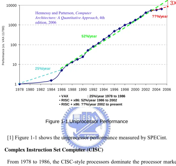
1 10 100 1000 10000 1978 1980 1982 1984 1986 1988 1990 1992 1994 1996 1998 2000 2002 2004 2006 Per for m anc e ( v s . VAX-11/ 780) 25%/year 52%/year ??%/year • VAX : 25%/year 1978 to 1986 • RISC + x86: 52%/year 1986 to 2002 • RISC + x86: ??%/year 2002 to presentHennessy and Patterson, Computer
Architecture: A Quantitative Approach, 4th
edition, 2006
3X
Figure 1-1 Uniprocessor Performance
[1] Figure 1-1 shows the uniprocessor performance measured by SPECint. Complex Instruction Set Computer (CISC)
From 1978 to 1986, the CISC-style processors dominate the processor market. The essence of CISC is to allocate as many hardware as the functions need. Therefore, the CISC processors can perform some specific functions at high speed.
But CISC processors have some well-known drawbacks.
Instructions of CISC processors have very different execution cycles. Single instruction may consume cycles from several to thousands corresponding to its functionality and complexity. The complexity of instruction variation and hardware selection lead to the inefficiency of the compiler. Besides, If pipeline technique is coordinated to boost the performance of CISC processors, it would be hard to pipeline, and the improvement of performance is limited.
In addition, all CISC-style processors suffer a serious problem. Some hardware is idle at most time. DEC-PDP 10 is a famous CISC processor, and some surveys [2] of this processor tell us that 70 instructions account for 99% of operation and 50 instructions account for 95% of operation. Lots of instructions and hardware are rarely used, and the idle hardware implies the waste of power consumption.
Simple scalar, Reduced Instruction Set Computer (RISC)
In 1980s, the RISC concept showed up. The essence of RISC is to handle single function within single instruction. Figure 1-2 is an example of RISC, simple scalar. Designers only deploy some primitive hardware to maintain its functionality. All the instructions of RISC have same instruction length, so it is easy to pipeline. Moreover, the performance can be easily enhanced along with the advance of technology. Using some instruction encoding techniques can raise the performance, too. Because of the regularity and simplicity of RISC, it has been widely spread out.
Figure 1-2 Scalar
Here are some disadvantages of RISC processors. The RISC processors have a low hardware utilization problem. They operate one function in single instruction, their hardware utilization is 1. When the number of primitive functional units increases, the low utilization characteristic remains unchanged. What is more, the RISC needs to fetch operands from register or memory first. After perform the single operation, the RISC needs to store the data into register of memory. The accesses per operation of the RISC is very high. It implies the power inefficiency.
Multi-issue (VLIW)
Multi-issue is opposite to single-issue. It means that multiple instructions issued at the same time. The most popular type called Very Long Instruction Word (VLIW) stands for the multi-issue processors since it has been proposed in 1980s. Figure 1-3 shows a 3-way VLIW and a 4-way VLIW.
Figure 1-3 VLIW
The VLIW processors exploit the instruction level parallelism (ILP). The functional units operate concurrently. It can reach high performance by taking advantage of ILP.
The greatest problem of VLIW is the register file pressure. Because the VLIW perform multiple functions in the mean time, each functional unit needs corresponding read or write ports to the register file. The port number strongly affects the area of register file. According to [3], in full custom design, for N FUs, area and delay are increases as N 3 and N 3/2. Besides, the same frequency of register or memory accesses with RISC processor makes the power inefficiency problem remained.
Finally, the performance can’t be raised infinitely due to the ILP has its limit. Some other processor architectures are taken into consideration.
Multi-core
After 2000, the performance of VLIW is no longer sufficient for some specific application.
Multi-core processors use several homogeneous or heterogeneous processors to do things at the same time. Hence the higher performance can be achieved. In this thesis, we only concern about the single core processor. The multi-core issue is beyond the scope.
Multi-threaded
[4] In unending quest for computers with higher performance, computer system architects seek to reduce or hide latency, the number of cycles an operation takes from start to finish. A long latency may extend for 10 to 100cycles, forcing the traditional processor to sit idle until the result comes in. Less time is wasted if the latency is reduced or even hidden behind the ongoing execution of another operation.
A popular means of reducing latency is the on-chip cache memory, which can shorten the round trip to data storage from tens of cycles to just one or two. Multithreaded architectures, however, take the tack of hiding latency by supporting multiple concurrent streams of execution, or threads, which are independent of one another. The threads are interleaved on a single processor. When a long-latency operation occurs in one of the threads, another begins execution. In this way, useful work is performed while the time-consuming operation is completed.
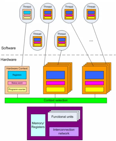
Figure 1-4 shows the multithreaded architecture. It includes several parts including computing, selection network, hardware and software context (threads)…etc. The computing part is composed of some functional units, memory/registers, and some interconnection network. Threads are mapped onto hardware context, which each include general-purpose registers, status registers, and a program counter. One context represents a running thread, while the others represent
threads that are eligible to run or are waiting on an operation to complete. Because of hardware limits, some threads are not currently mapped. The functional units handle the operations. The memory/registers store some intermediated value to accelerate the whole works. The interconnection network and the context selection hardware maintain the accuracy of each interleaved thread.
Figure 1-4 Multithreaded architecture
Multi-threaded architectures take advantage of thread level parallelism. Three categories of multi-threaded architectures are coarse-grained multithreading, fine-grained multi-threading, and simultaneous multithreading [5].
z Coarse-grained (block) multithreading (BMT)
The simplest type of multi-threading is where one thread runs until it is blocked by an event that normally would create a long latency stall. Such a stall might be a cache-miss that has to access off-chip memory, which
might take hundreds of CPU cycles for the data to return. Instead of waiting for the stall to resolve, a threaded processor would switch execution to another thread that was ready to run. Only when the data for the previous thread had arrived, would the previous thread be placed back on the list of ready-to-run threads.
z Fine-grained (interleaved) multithreading (IMT)
A higher performance type of multithreading is where the processor switches threads every CPU cycle. The purpose is to remove all data dependency stalls from the execution pipeline. Since one thread is relatively independent from other threads, there's less chance of one instruction in one pipe stage needing an output from an older instruction in the pipeline.
z Simultaneous multithreading (SMT)
The most advanced type of multi-threading applies to superscalar processors. A normal superscalar processor issues multiple instructions from a single thread every CPU cycle. In Simultaneous Multi-threading (SMT), the superscalar processor can issue instructions from multiple threads every CPU cycle. Recognizing that any single thread has a limited amount of instruction level parallelism, this type of multithreading is trying to exploit parallelism available across multiple threads to decrease the waste associated with unused issue slots.
SMT is the most complex because of the functionality among threads must be maintained. The most regular is IMT. By the way, the IMT can totally hide instruction latency if enough threads are supported. The hardware cost of IMT, since there are more threads being executed concurrently in the pipeline, shared resources such as caches and TLBs need to larger to avoid thrashing between the different threads. In this thesis, our hide instruction latency technique will focus on IMT.
1.2 Proposed Composite FUs and Contributions
In order to solve the problems mentioned above, we proposed the Composite FUs with the purposes listed below.
Application-specific composite FUs
Composite FU is a cascade datapath. It cascade several primitive FUs to form a composite datapath. Analyze the characteristic of specific application, and find out what operations can be combined into single instruction.
High hardware utilization and high OPs/access
Compared with the RISC processors, the composite FUs perform several functions in single instruction. It means that composite FUs do more things than RISC in a period of time. Hence, the hardware utilization improves.
Besides, the RISC needs a lot of accesses from register or memory. The composite FUs fetch proper operands and perform several operations, then store back to the register or memory. So the total number of accesses is reduced. Register access is a power-consuming action. The composite FUs have high OPs/access that lead to power efficiency potential.
Low register file pressure (limited R/W ports)
Port number Scalar Compostie FUs VLIW 3FUs 2R/1W 3R/1W 5R/3W 4FUs 2R/1W 4R/1W 7R/4W Table 1-1 Port number of different datapaths
The port number of composite FUs increases one or remains unchanged as the FU number increase. Not like the VLIW processors, every FU needs two or three ports. So the grow-up trend of port number is larger in the VLIW than in the
composite FUs. Fewer ports of the composite FUs ease off the register file area pressure. The example of port number is shown in Table 1-1.
Suitable for IMT DSP (zero instruction latency)
When we want to reach higher performance, we will introduce our pipeline design to boost performance. Once the pipeline technique has been used, the instruction latency issue must be taken into consideration. If we ignore the pipeline latency, the data accuracy may have errors. If we just wait until the last work ready, then the performance can’t be raised ideally.
There are some techniques to reduce or hide instruction latency, either from software or hardware view. Software method including loop unrolling, software pipelining, etc. and hardware method including forwarding, multithreaded architectures, etc. are all possible solutions.
In this thesis, we choose the IMT architecture to be the way of hiding instruction latency because of it can totally hide instruction latency. And the hardware cost of the composite FUs coordinated with IMT is not much. IMT needs a thread register file for each thread, the register file cost of the composite FUs is acceptable.
1.3 Thesis Organization
The rest of this thesis is organized as follow.
Chapter 2 introduces the background of our work. First, we talk about what is the composite FUs. Second, describe the meaning stand for data flow graph (DFG) and its components. Third, show a covering and match method called ID-based search graphs. Fourth, show the scheduling procedures using list scheduling based method. Fifth, introduce a RF model to estimate the area of register files. Last, illustrate how the interleaved multithreaded (IMT) architecture work.
Chapter 3 describes the comparison of the advantage and disadvantage among scalar, VLIW and Composite FUs from the area and power experiment. For high performance, we have a pipeline designer to speed up the processor with the composite FUs. And we use the IMT architecture to hide instruction latency completely.
Chapter 4 states the difference between classic and our ASIP synthesis flow. Then we propose a flow to recommend a proper composite FU for ASIP designer under certain constraints.
Finally, chapter 5 concludes this thesis and points out the direction for the future researches.
2 Background
First at all, we will give a simple illustration of the composite FUs and talk about how it works.
The composite FUs take the advantage of application characteristic. We must develop a software tool chain to analyze the applications and to find out the possibility of operation combination. We will introduce the format that we concern, DFG. Then use covering and matching technique to recognize new operations after merging. Next, we want to estimate the area of the register files. So we use a list scheduling based method to find a sub-optimal register requirement. Then the estimation is done through a RF model method related to the technology process.
We want to further speed up the performance using pipeline design. It introduces extra instruction latency problem. As mentioned before, we use IMT to hide solve the problem. So we will show how IMT works at the last of this chapter.
2.1 Composite FUs
We propose the composite FU which cascades all the primitive FUs in a customized order by analyzing the DFG (data-flow graph) of the target applications.
A composite FU is a cascade datapath. Figure 2-1 illustrates a MAS composite FU that cascades a multiplier with an adder and then a shifter. On each instruction issue, the maximum number of operations is three, i.e. multiplying operand 1 by operand 2 and then adding the result to operand 3 and finally shifting the sum by a specific value, while the minimum number is one, i.e. either one multiplication or one addition or one shift.
Figure 2-1 Composite FU: MAS
Primitive Operation Set
For simplicity, we define a primitive operation set with three kinds of primitive operations including adder, multiplier, and shifter. Figure 2-2 shows the configuration of (a) adder, (b) multiplier, and (c) shifter.
A M S
Dest Dest Dest
Src1 Src2
Add/Sub
Src1 Src2 Src1
Shamt
(a) (b) (c)
The adder and multiplier both have two source operands and one destination. On the other hand, the shifter only has one source operands and one destination. There is a Add/Sub control signal to tell the adder to perform addition or subtraction. The shifter has a Shamt control signal to decide right shift or left shift and shift amount.
The applications which we analyze in the rest part of this thesis are all based on this primitive operation set.
Port constraint
Port number restricts the possible arrangement of the composite FUs.
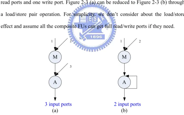
Figure 2-3 (a) is a full read/write ports version of composite FU MA. It has three read ports and one write port. Figure 2-3 (b) is a reduced version, and it has two read ports and one write port. Figure 2-3 (a) can be reduced to Figure 2-3 (b) through a load/store pair operation. For simplicity, we don’t consider about the load/store effect and assume all the composite FUs can get full read/write ports if they need.
M A M A 1 2 3 1 2
3 input ports 2 input ports
(a) (b)
Figure 2-3 Composite FU: MA with (a) full R/W ports (b) reduced R/W ports
There are some techniques used in Sandblaster processors [6] to reduce the number of ports if the hardware doesn’t need it at the same time, but it has extra huge overhead to guarantee the accuracy.
2.2 Data-Flow Graph
In mathematics and computer science, graph theory is the study of graphs; mathematical structures used to model pair-wise relations between objects from a certain collection. A "graph" in this context refers to a collection of vertices or 'nodes' and a collection of 'edges' that connect pairs of nodes. A graph may be undirected, meaning that there is no distinction between the two nodes associated with each edge, or its edges may be directed from one node to another.
[7] The data-flow graph captures the data-driven property of DSP algorithm where any node can fire (perform its computation) whenever all the input data are available. It means that a node with multiple input edges can only fire after all its precedent nodes have fired. In data-flow graph (DFG) representations, the nodes represent computations (or functions or subtasks) and the directed edges represent data paths (communications between nodes).
Definition
Node N: computations Edge E: data dependencies Graph G = { N, E }
The precedence constraints specify the order in which the nodes in the DFG can be executed. Different representations of the same algorithm may lead to different DFG.
Figure 2-4 is a DFG example of 8 points 1D discrete cosine transform in Lee’s algorithm [8].
A0 A1 A2 A3 A4 A5 A6 A7 M0 M1 M2 M3 A9 A12 A10 A11 A8 A13 A14 A15 -1 -1 -1 M4 M5 M6 M7 A18 A19 A16 A17 -1 -1 A20 A21 -1 A22 A23 -1 M8 M9 M10 M11 A24 A25 A26 A28 A27 X0 X4 X2 X6 X1 X5 X3 X7 S1 S2 S3 S4 S5 S6 S7 S8 -1 -1 -1 -1 -1 S0
Figure 2-4 DCT (Lee’s algorithm)
DFG Description
For convenience, we make a DFG description. The complete DFG includes input/output part and the pure operation part. In our analysis, we suppose the load/store decoupled.
z Input/Output Part
I# (# stands for the number)
O# Src1 (Src1 is the source of output node)
z Operation Part
1. Addition/Subtraction
Syntax: A# Src1, Src2, addsub
Description:
Get Src1 and Src2 data from corresponding node and perform addition or subtraction. The addsub field stands for what the operation the adder does. “+” is for addition, and “-” is for subtraction.
2. Multiplication
Syntax: M# Src1, Src2
Description:
Get Src1 and Src2 data and perform multiplication.
3. Shift
Syntax: S# Src1, shamt
Description:
Get Src1 data into register Src1 and shift by shamt-bit. The Shamt fields stand for shift amount and ranges from -8 to 7. The shamt is a 4-bit field supporting up to 8-bit left and 7-bit right shift.
z Example
Figure 2-5 illustrates an example of DFG description of first order biquad filter.
I0 I1 I2 I3 I4 I5 I6 I7 I8 I9 I10 I11 A0 M0,M1,+ A1 M2,M3,+ A2 M4,M5,+ A3 I0,A0,-A4 I1,A1,-A5 I2,A2,-A6 M6,M7,+ A7 M8,A6,+ M0 I3,I7 M1 I4,I8 M2 I4,I7 M3 I5,I8 M4 I5,I7 M5 I6,I8 M6 A3,I9 M7 A4,I10 M8 A5,I11 O0 A7 I0 x0 I1 x1 I2 X2 I3 w0 I4 W1 I5 w2 I6 w3 I7 a1 I8 a2 I9 b0 I10 b1 I11 b2 M0 M1 M2 M3 M4 M5 A0 A1 A2 A3 A4 A5 M6 M7 M8 A6 A7 O0Y0
2.3 Covering
In the mathematical discipline of graph theory a covering for a graph is a set of nodes (or edges) so that the elements of the set are close (adjacent) to all edges (or nodes) of the graph. We are especially interested in finding small sets with this property. The problem of finding the smallest node covering is called the node cover problem and is NP-complete.
Figure 2-6 Covering and supernode
Figure 2-6 shows a supernode merges several nodes together. It inherits the functionality and the dependencies of the replaced nodes.
A perfect matching is a matching which covers all nodes of the graph. We want to find a perfect matching of the application using the composite FUs.
Unate and binate covering problems [9]
The classical solving approach for two-level logic minimization in the VLSI literature goes back to Quine’s and McCluskey’s works. It reformulates the problem as a special case of the Unate Covering Problem [10] and applies algorithms conceived for the latter, or even for the more general Binate Covering Problem.
Binate (or unate) covering problems is a well known intractable problem. It has several important applications in logic synthesis, such as two-level logic minimization, two-level Boolean relation minimization, three-level NAND implementation, state minimization, exact encoding, and DAG covering [11].
The next paragraph briefly defines the binate covering problem and the notations of typical presentation.
Let f (y1, …, yn) be a Boolean function from {0, 1}n into {0, 1}. Let Cost be a
function that associates a positive cost with the assignment of variable yk to 0 or 1.
The cost of a n-tuple (v1, …, vn) of {0, 1}n is defined as
∑
=n
k 1Cost (yk = vk).
Definition (Binate covering problem)
The binate covering problem (also called minimum cost assignment problem) consists of finding a minimal cost n-tuple that values f to 1.
z Node covering
[12]When deliveries, collections, or visits must be made to (or from) a number of specific (and, often, widely separated) points, the routing problem that must be solved becomes a node-covering one. The demand (or supply) points can then be represented as the nodes on the network model of the urban transportation grid and the question of the order in which to visit these nodes so as to achieve some objective is then addressed.
Our goal is similar to two-level expression, and it is a binate covering problem. [13] The difference is that our operations are not simple logic gates, but three primitive operations, including adder, multiplier, and shifter. There are some studies of the binate covering. We use a covering method called ID-based search graph proposed in IBM’s research [14] and make some modification to facilitate our analysis.
ID-based search graph
A crucial step in the design of Application-Specific Instruction-set Processors (ASIPs) [15] is the instruction-set generation. Methods for automating this process, surveyed in, extract patterns from applications, usually in the form of data-flow graphs, and insert them into a pattern library.
The ID-based search graph introduce a novel organization for pattern libraries that enables a search algorithm with only O(d), where d is the size of the pattern sought up to the maximum pattern size in the library. Furthermore, the library organization reveals opportunities to substitute one pattern by another. This may be exploited for more efficient instruction selection and code generation. The method is presented for tree-shaped patterns but can be extended to directed acyclic graphs (DAGs).
z Organizing libraries as identity graphs
In order to create match libraries for a specific application, we decompose the pattern which is used to compare with the application into several sub-levels. Figure 2-7 illustrates the procedures of ID-based search graph to organize libraries. The basic 3-levels pattern is AND-SHR-SUB. It covers an addition, a shift, and a abstraction. The sub-functions of level 2, level 1, and level 0 can be derived from by-passing some functions.
z Searching an ordered library
In order to find all matches, match all the nodes from the highest level to lowest level because of the higher level function or sub-functions can perform more operations in single instruction and execution.
2.4 Scheduling
To estimate the area of register files, we must analyze the register requirement first to find the scale of register numbers. Scheduling and resource allocation can help us to understand the register requirement. In this section, we talk about the basic idea and steps of scheduling first.
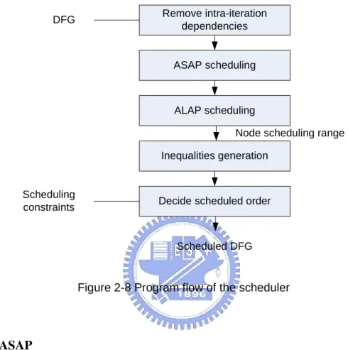
[7] Scheduling is to assign the nodes on the DFG to be processed by which functional unit in which time step. Our scheduler schedules the target DFG. Figure 2-8 shows the program flow of the scheduler. Here, we use periodic scheduling for simplicity, where only the intra-iteration data dependency is considered and the edges with delay elements (i.e. dependency across iterations) are removed from DFG first. Then we will make a lifetime analysis of every node. The DFG is scheduled with the ASAP (as soon as possible) and ALAP (as last as possible) scheduling algorithm to
obtain the range to schedule each node. Then, we apply some list scheduling based methods to the steps. At last, the scheduled DFG is output and the register requirement is reported. Remove intra-iteration dependencies ASAP scheduling ALAP scheduling Inequalities generation
Decide scheduled order DFG
Scheduling constraints
Scheduled DFG
Node scheduling range
Figure 2-8 Program flow of the scheduler
ASAP
ASAP (as soon as possible) is one of the earliest and simplest scheduling algorithms. ASAP scheduling assumes that the hardware resource (functional units) is unlimited. Nodes are first topologically sorted, that it, if a node nj is constrained to
follow the node ni with a precedence constraint, then nj will topologically follow ni.
From the sorted list, nodes are taken one at a time and placed in the earliest available time step, depending on its precedence constraint. Figure 2-9 shows the algorithm of ASAP scheduling. The ASAP scheduling is used to determine the earliest scheduling bound of each node.
INPUT: SDFG G=(N,E)
OUTPUT: ASAP SCHEDULE
TS0=1; //SET INITIAL TIME STEP
WHILE (UNSCHEDULED NODES EXIST) {
SELECT A NODE NJ WHOSE PREDECESSORS HAVE ALREADY BEEN SCHEDULED; SCHEDULE NODE NJ TO TIME STEP TSJ = MAX {TSI+(CI)} FOR ALL NI Æ NJ; }
Figure 2-9 The ASAP scheduling algorithm
ALAP
ALAP (as late as possible) scheduling is similar to the ASAP scheduling; except for the way nodes are placed in the schedule. As the name indicates, ALAP scheduling in Figure 2-10 builds the schedule bottom up and the nodes are topological sorted in reversed order. Therefore, the algorithm must have the information of the iteration period to build the schedule from the bottom up and the iteration period must be long enough to allow all the nodes to be scheduled, otherwise the scheduling will fail.
INPUT: SDFG G=(N,E), ITERATION PERIOD:T OUTPUT: ALAP SCHEDULE
TS0=T; //SET TIME STEP
WHILE (UNSCHEDULED NODES EXIST) {
SELECT A NODE NJ WHOSE SUCCESSORS HAVE ALREADY BEEN SCHEDULED; SCHEDULE NODE NJ TO TIME STEP TSJ = MAX {TSI-(CI)} FOR ALL NI Æ NJ; }
ILP-based scheduling
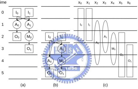
After the ASAP and ALAP scheduling, we describe and solve the scheduling problem by inequalities and priorities. Figure 2-11 gives examples of ASAP, ALAP, and the scheduling range from ASAP and ALAP. When constructing inequalities for constraints, each position (i.e. node i at the time step j) in the range are associated with a Boolean variable xi.j which indicates whether a node i is scheduled into the time step j. The following four constraints must be satisfied.
I0 I1 O0 A1 O1 A0 M0 I0 I1 O0 A1 O1 A0 M0 I0 I1 A0 A1 M0 O0 O1 (a) (b) (c) 0 time 1 2 3 4 5 x0 x1 x2 x3 x4 x5 x6
Figure 2-11 Scheduling example (a) ASAP (b) ALAP (c) scheduling range
1. Resource constraints
This constraint states that no schedule will have a time step that contains more operations than the available functional units due to the limited hardware resources. Because we assume that the I/O unit and adder are all of one, the inequalities for this constraint of the example in Fig. 2-11 (c) should be:
x0.0+ x1.0 ≤ 1; x0.1+ x1.1 ≤ 1; x0.2+ x1.2 ≤ 1 (for input) x2.1+ x3.1 ≤ 1; x2.2+ x3.2 ≤ 1; x2.3+ x3.3 ≤ 1 (for adder) x + x ≤ 1; x + x ≤ 1; x + x ≤ 1 (for output)
2. Allocation constraints
This constraint states each node can only be scheduled within the scheduling range bounded by some range obtained from the ASAP and ALAP scheduling and can only appear once in the schedule. The inequalities for this constraint of the example in Fig. 2-11 (c) should be:
x0.0+ x0.1+ x0.2 = 1 x1.0+ x1.1+ x1.2 = 1 x2.1+ x2.2+ x2.3+ x2.4 = 1 x3.1+ x3.2+ x3.3 = 1 x4.2+ x4.3+ x4.4 = 1 x5.2+ x5.3+ x5.4+ x5.5 = 1 x6.3+ x6.4+ x6.5 = 1 3. Dependency constraints
The data dependency in the original DFG should be strictly followed when scheduling. The dependency constraint ensures that DFG remains causal and correct timing sequence. The inequalities for this constraint of the example in Fig. 2-11 (c) should be: x0.0 + 2 x0.1 + 3 x0.2 - 2 x2.1 - 3 x2.2 - 4 x2.3 - 5 x2.4 ≤ -1 x1.0 + 2 x1.1 + 3 x1.2 - 2 x2.1 - 3 x2.2 - 4 x2.3 - 5 x2.4 ≤ -1 x0.0 + 2 x0.1 + 3 x0.2 - 2 x3.1 - 3 x3.2 - 4 x3.3 ≤ -1 x1.0 + 2 x1.1 + 3 x1.2 - 2 x3.1 - 3 x3.2 - 4 x3.3 ≤ -1 2 x2.1 + 3 x2.2 + 4 x2.3 + 5 x2.4 - 3 x5.2 - 4 x5.3 - 5 x5.4 - 6 x5.5 ≤ -1 2 x3.1 + 3 x3.2 + 4 x3.3 - 3 x4.2 - 4 x4.3 - 5 x4.4 ≤ -1 3 x4.2 + 4 x4.3 + 5 x4.4 - 4 x6.3 - 5 x6.4 - 6 x6.5 ≤ -1
4. Port conflict constraints
If the functional units are consisted of single-write instead of N-write memory or registers to reduce the hardware complexity, it may introduce port conflicts when multiple functional units simultaneously write their results into the same memory or registers. We can schedule the operations with an identical destination memory or registers into different time slots by incorporating the following port constraints to prevent conflicts. The inequalities for this constraint of the example in Fig. 2-11 (c) should be:
x0.0+ x1.0 ≤ 1; x0.1+ x1.1 ≤ 1; x0.2+ x1.2 ≤ 1; (for adder) x2.2+ x4.2 ≤ 1; x2.3+ x4.3 ≤ 1; x2.4+ x4.4 ≤ 1; (for output)
According to the assumption above, the composite FUs discussed in this thesis have full read/write ports. The port conflict constraints are mapped to the different situations.
2.5 Complexity of Synthesized Register File
We want to compare the RF area of the composite FUs with the RF area of the VLIW. We need a roughly estimation method to see the scale and the pressure of the RF area. Here is a survey of the relations among RF area and the FU number and port number in [16], and it proposes a simple RF model for 0.18 um process.
Conventionally, the microprocessors have a more efficient and direct data exchange mechanism among the parallel FUs through the register file (RF) than the multi-processors, where a monolithic and centralized RF provides storages for and interconnects to each FU in a general and homogeneous manner. However, the complexity of the centralized RF grows with the number of access ports increasing.
In centralized RF, every read port and write port can directly access any registers in the RF. Prior art has evaluate the complexity of centralized RF in full-custom designs.
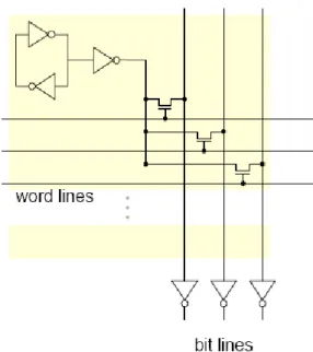
The RF consists of register cells similar to SRAM. Generally, the register cell is organized as 6-transistor structure, and the access port of RF requires a word-line and a bit-line which is shown in Figure 2-12. Therefore, the area of single SRAM cell grows in two dimensions and can be described as P2. For a full-custom centralized RF with n-registers and P-ports, the area and delay are approximated to n×P2 and n1/2×P respectively [3].
Figure 2-12 A register cell in full custom design
The number of registers and ports required can be estimated from the number of FUs. Assume that each FU requires two ports for two source operands and one port to write the result back to RF, and every FU requires at least one register to store the manipulated data. Consequently, for N FUs, the number of registers and ports is approximated to N and 3N respectively. As a result, the area and delay are increases as N 3 and N 3/2.
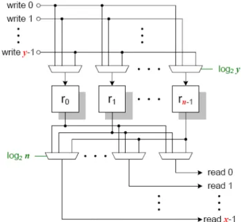
In this thesis we focus on the cell-based RF organization which consists of flip-flops and switch networks. For a centralized RF with N registers, x read ports, y write ports, and word length W, the complexity of read access network is an N to x crossbar router and every read port has one N to 1 multiplexer. Similarly, the complexity of write access network will be y to N crossbar router with y to 1 multiplexer for each register elements. Figure 2-13 shows the access network of a centralized RF.
Figure 2-13 Access network of centralized register file
The output of each register has to drive x × N-to-1 multiplexers which results in a very high output loading capacitance. The centralized RF is efficient when executing program with high data-level parallelism only. But it is difficult to guarantee the data-parallelism level of applications, so it is unnecessary to provide the bandwidth for non-common cases with the cost of RF access time and RF area.
We roughly evaluate the area and speed of centralized RF based on the architecture shown in Figure 2-13. The cost function of area complexity for centralized RF is analyzed as follows:
fA CRF (x, y, N, W) = Awrite_network + Aread_network + Aregisters + Acontrol
≅ [N × Ay-to-1_mux + x × AN-to-1_mux + N × AD-flipflop] × W
≅ [N × (y – 1) × A2-to-1_mux + x × (N - 1) × A2-to-1_mux
+ N × AD-flipflop] × W
This Function assumes all multiplexers are composed of 2-to-1 multiplexers and the control overhead is neglected. This analytical formula is also based on the number of 2-to-1 multiplexers on data path. The experimental results show the analysis is close to synthesis result. Table 2-1 compares the analytical analysis with synthesis results using TSMC 0.18um cell library in different centralized RF configurations. In this thesis, the discussion of timing estimation is out of scope.
The area of analytical results is based on the cell library. The constraint of synthesis is optimized for area to avoid the variance due to the timing optimization technique. The area is over estimated in 16-entry, 1R1W configuration because of the 2-to-1 multiplexer model is actually larger than 4-to-1 multiplexer cell that synthesis tool uses. From the analysis, we can sum up that the area of cell-based CRF is direct proportion to both number of registers and number of ports and the synthesis results prove the point. The natural of high routing complexity of RF will cause high variance in physical implementation, and the variance growing with the number of registers and ports increasing.
2.6 Interleaved Multithreaded (IMT) Architecture
When we use pipeline design to boost the performance of the composite FUs, it will introduce instruction latency. This section shows how the IMT architecture hides the instruction latency totally.
Figure 2-14 illustrates an example of the interleaved threads and dependencies in the pipeline. If an IMT architecture processor has 5 stages and the pipeline latency is 5 cycles, it needs 5 interleaved threads to hide instruction latency totally. These 5 threads are independent tasks.
The operation is to issue the first instruction of thread 1 at cycle 1 into the pipeline, then issue the first instruction of thread 2 at cycle 2, and so on. After first iteration from thread 1 to thread 5 is done, issue the second instruction of thread 1. In this way, the following iterations are executed.
Figure 2-14 Interleaved threads and dependencies in the pipeline
The first instruction and second instruction of thread 1 may have dependency. In the original pipeline design, if their execution time is overlapped, there would be some kind of data hazard. So it must stall the second instruction until the first instruction complete, but this handling method hinders the speedup of performance.
As Figure 2-14, interleaved threads method solves the problem. The execution time of first and second instructions has no overlapped. It hides the instruction latency without any performance loss.
3 The Composite FUs
We want to quantify the hardware utilization of the composite FUs. Once the hardware utilization is upgraded, we analyze the area pressure of register file for different datapaths under different performance constraint.
In section 3-1, we introduce the composite FUs generator to analyze the operations per cycle of all kinds of composite FUs running different applications. After then, the register requirement and the estimated area of register files is calculated by the method in section 2-5 with small modification. Afterward, use pipeline design to boost performance. The pipeline design flow is described in section 3-2. Because of the pipeline design introduces instruction latency, the IMT is used for pipelined composite FUs. We will talk about the hardware cost of IMT.
As a result of operands operated for more than one operation after being fetched, the total register accesses are reduced. We also estimate the power consumption to see where the power is saving.
3.1 The Composite FUs Generator
Figure 3-1 The composite FUs generator
We introduce the composite FUs generator in Figure 3-1 for application analysis. When the composite FUs generator receives a FU resource constraint and an application in DFG description, three recursive steps have been taken iteratively.
First, select an arrangement from possible candidate formed by FU resource constraint. Second, create an ID-based search graph and match libraries of the arrangement and cover the DFG using the function set of the arrangement. Finally, the register requirement is calculated for further area estimation.
Repeat these steps until all the case of arrangements are done, we can get operations per cycle (OPC) and register requirement for each composite FU. The composite FU with best OPC implies the most proper datapath and the hardware utilization is the highest for the application.
3.1.1 Arrangement Space
For given FU resources, there are many arrangements to form a composite FU. Number of functional units: N
Number of adders: NA
Number of multiplier: NM
Number of shifter: NS
The total arrangements:
! !* !* ! S M A N N N N S =
In this thesis, we concern about two cases of function units set. One is 3 FUs composed of 1 adder, 1 multiplier, and 1 shifter. The other is 4 FUs composed of 2 adders, 1 multiplier, and 1 shifter. For the former case, NA = 1, NM = 1, NS = 1, so the total arrangements S is 6 as Figure 3-2 shows. For the latter case, NA = 2, NM = 1, NS = 1, so the total arrangements S is 12 as Figure 3-3 shows.
Figure 3-2 The arrangement space of 1 A 1M 1S
3.1.2 ID-based Search Graph Covering
According to section 2-3, we map the ID-based search graph from Boolean expression to the analysis of the composite FUs. We use exhaustively tree-structured search principle to simplify selected composite FU.
Figure 3-4 The ID-based search graph of MAS
Figure 3-4 illustrates composite FU: MAS and its sub-level functions. First, the MAS-ordered composite FU is categorized into 3 levels of operations. That is, level-3 operation, MAS, performs one multiplication, one addition plus one shift serially. Level-2 operations, including MA, AS, and MS, perform either one multiplication and one addition, or one addition and one shifter, or one multiplication and one shifter serially. Level-1 operations, including M, A, and S, perform either one multiplication, one addition or one shift serially. We can use adding zero, multiplying by one and shifting by zero to bypass the adder, the multiplier and the shifter respectively.
Then, the ID-based covering is performed to cover the nodes of the input DFG by available operations, i.e. level-3, level-2 or level-1 operations. Note that, all covered nodes are assumed to consume one clock cycle. The covering process first searches the whole DFG for any pattern that is matched to the level-3 operation and then for any remaining uncovered node patterns that are matched to the level-2 operation and so on.
Multiple Fan-out Handling and Optimization
z Multiple fan-out problem
Figure 3-5 (a) shows a DFG of a butterfly application, we use Figure 3-5 (b), composite FU: AMAS to cover this DFG. If the A0-M0-A2 is merged together when the match is proceeding in level 3 match for AMA, one of the A3 node can’t get the data from M0 node because of the composite FU AMAS don’t have a write port after multiplication to store the right value into the register file. Hence, the application cannot be fulfilled. Some actions must be taken to prevent the hazard from happened.
Figure 3-5 (a) a DFG of butterfly (b) the composite FU: AMAS
z Break
The simplest method to avoid the data hazard is to break at the multiple fan-out nodes. Figure 3-6 illustrates the procedures. The level 2 AM function matches A0-M0 and A1-M1 to form new nodes C1 and C3. The level 1 A function matches A2 and A4 to form new nodes C2 and C4. It takes 4 nodes to perform the butterfly.
Figure 3-6 Break at multiple fan-out node
z Node duplication
For optimization, we use the node duplication technique to minimize the number of matches. Figure 3-7 (a) shows the spirit of node duplication. Breaking at M0 to let A3 get correct source value needs a instruction for A3 only. But we can repeat the operation A0-Mo in the same instruction with A3 because the characteristic of the composite FU allows these work done in the same instruction.
Figure 3-7 (b) illustrates the procedures. The level 3 AMA function matches A0-M0-A2 and A0-M0-A3 to form new nodes C1 and C2. The level 2 AM function matches A1-M1 to form new node C3. It only takes 3 nodes, equals 3 instruction for execution, to perform the butterfly. The node duplication technique reduces the nodes of the covering result form 4 nodes to 3 nodes.
Figure 3-7 Node duplication at multiple fan-out nodes (a) covering (b) duplicate A0 and M0
3.1.3 Scheduling
Since we want to estimate the area of register files, the scheduling principles with optimizing for register requirement are chosen. But finding out the minimum register requirement is a NP-complete problem. So we use two simple scheduling to get the sub-optimal solution. Some concepts are from [17], forced-directed list-scheduling [18], loop-list scheduling [19], and cone-base list-scheduling [20].
Lifetime Analysis
Based on section 2-4, the lifetime analysis about ASAP scheduling, ALAP scheduling, and range estimation is done first. Then we construct resource, allocation, dependency, and port conflict constraints. With these inequalities, we can put some priorities to solve the linear programming problem and make the scheduled order.
Cutsets
Cut the DFG into branches, called cutsets which have no dependencies of each other. Figure 3-8 cuts the DFG into three independent cutsets. Give the independent cutsets different priorities and finish the cutset one by one can minimize the live registers at the same time space.
Figure 3-8 Cutset of DFG
For example in Figure 3-8, assume that only one node can be executed in one cycle because of limited hardware resource, and the hard deadline of the whole
application is 10. The range of lifetime analysis of each node is listed in the square bracket near the node. The value before comma is the earliest time step of ASAP scheduling, and the other value after comma is the latest time step of ALAP scheduling. Node 1 in cutset 1, node 3 in cutset 2, and node 7 in cutset 3 have the same lifetime. It means that their live ranges are completely the same. Without cutset priorities, the scheduling result of cycle 1 is node 1, cycle 2 is node 3, and cycle 3 is node 7, and so on. The register requirement is 3 which happened to store intermediate value of node 1, 3, and 7. On the contrary, set cutset priorities 1 to nodes of cutset 1, 2 to nodes of cutset 2, and 3 to nodes of cutset 3. The scheduling result of cycle 1 is node 1, cycle 2 is node 2, cycle 3 is node 3, and so on. The register requirement is only 1, either store 1, 3, or 7. The register requirement is reduced.
Priorities
Our resource is only one composite FU, if refines the resource constraint. We give different priorities for the independent cutsets first, then execution priorities. We use two methods to get the scheduled order and take the smaller register requirement as result. Additionally, if all the priority is the same, we will do the node with smaller serial number from the DFG description.
Scheduling 1
Based on the first come first serve principle, the execution priority setting start according to the ASAP result. Search the time space of ASAP and mark its order if its ancestor nodes are all in ready list.
Scheduling 2
If the timing constraint is critical, the deadline of each node is highly notified. The execution priority setting start according to the ALAP result, search the time space of ALAP and mark its order if its ancestor nodes are all in ready list.
Example
Step 2. ID-based Covering
A M A S M S M A S A M S A M S Level-3 Level-2 Level-1 M M M M M M A A A S A A M M M A A C6 Cycle 0 Step 3. Scheduling M M M M M M A A A S A A M M M A A C1 C2 C3 C4 M M M M M M A A A S A A M M M A A C5 C6 C7 C8 C9 C10 M M M M M M A A A S A A M M M A A C0
Step 1. Function Decomposition
C1 Cycle 1 C8 Cycle 2 C5 Cycle 3 C7 Cycle 4 C10 Cycle 5
Figure 3-9 shows recursive steps of automatic composite FUs generation. The three steps are listed as follow.
z Step 1. Function decomposition
The MAS-ordered composite FU is decomposed into 3 levels because it has three functional units. Level-3 operation is MAS. The number of level-2 operations is 3 including MA, AS, and MS. The number of level-1 operation is 3 including M, A, and S. These 7 operations compose of match libraries.
z Step 2 ID-based covering
Covering procedures start from the matching of level-3 operation. It finds a MAS match and marks it in C0. Then the matching of level-2 operations starts, and it finds 4 matches and mark it in C1~C4. Finally, the matching of rest of nodes using level-1 operations and make up C5~C10.
z Step 3 Scheduling
After ASAP and ALAP, the lifetime analysis is done and the scheduling result is C6 in cycle 1, C1 in cycle 2, C8 in cycle 3, C5 in cycle 4, C7 in cycle 5, C10 in cycle 6, and so on. And the register requirement is calculated as well.
3.2 Pipeline Design Flow and Hardware Cost of IMT
After the composite FU generation, the pipeline design is performed to decide the required pipeline stages according to the target performance. For example, if the OPC of some specific composite FU is 1.5 regarding a specific application and the target performance is 600MOPS (million operations per second), the required operation frequency is 400MHz.
We use the Synopsys DesignCompiler synthesis tool incorporated with the design flow shown in [] to analyze the various pipeline stage sand the associated area cost. This flow also applies for scalar, VLIW as well as the composite FUs for area comparison in the experiment introduced later.
On the other hand, for analyzing the area cost of datapath and the pipeline registers, we use the pipeline design flow in Figure 3-10. First, if the target clock cycle is d (ns) and the desired number of pipeline stages is p, we pre-synthesize the purely combinational circuit, i.e. MSA, with the input-to-output delay of d*p (ns). Then, (p-1)-stage pipeline registers are attached to the output of the synthesized netlist which is imported into DesignCompiler to perform register retiming with the target clock cycle d (ns) as clock constraint. Finally, the resultant netlist is re-synthesized again and the area cost is recorded.
The main innovations of the pipelining design flow are two-folded. The first is to avoid a over-designed netlist. The conventional method that does not take the target clock rate and the desired number of pipeline stages into consideration may use a tight timing constraint to pre-synthesize the purely combinational circuit and thus results in a over-designed netlist of excessively large area. The other innovation of the proposed pipeline design flow can avoid the situation that insufficient pipeline stages will result in so tight clock timing constraint that the resultant netlist is of excessively large area. In our experience, under some cases, the synthesized netlist with more pipeline stages will has smaller area than that with less pipeline stages.
Hardware Cost of IMT
Because we use interleaved multithreading technique to hide pipeline latency, one more set of context, i.e. register file, is required for one more pipeline stage. Because the port number of the composite is slightly larger than scalar processors and greatly smaller than VLIW processors, the IMT architecture is suitable for the composite FUs. Comparatively, the heavy area pressure hinders the VLIW from using IMT architecture.
4 Application Specific
Programmable Processor Synthesis
In classic ASIP synthesis flow, programmers usually design the instruction set architecture (ISA) and micro-architecture first. Then the software programmers and hardware designers develop the software tool chain and hardware architecture according to ISA and micro-architecture separately. This flow starts from high level synthesis and forms a top-down design.
We propose an Application Specific Programmable Processor Flow in section 4-2 to explore the design space of the composite FUs. Then we describes a composite FU selection flow to help users to find out the most proper composite FU.
4.1 High Level ASIP Synthesis Flow
[21] shows typical procedures of high level synthesis. Some instruction set matching and selection techniques are described in [22][23] [24]. [25] introduces the critical path and data path optimization for ASIP design.
High-level synthesis takes some kind of behavioral description of the algorithm, available hardware resources, and a set of constraints and goals, to generate the hardware architecture in register-transfer level (RTL). The set of constraints and goals define the desired performance and characteristics of the final architecture. The most common constraints are area and performance constraints.
Area constrained problems means that given a set of resources (or functional units), try to implement the application using those resources such that it has the highest performance. This is known as resource-constrained scheduling.
The performance constrained problem is known as time-constrained
scheduling, where the designer is given a desired sample rate or iteration period and
the goal is to minimize the total area of the final architecture.
There are other goals during the synthesis problem depending on the user requirement such as minimizing the number of memory modules, reducing the power consumption, minimizing the number of busses, incorporating reliability and testability into the design, etc.
Language description of algorithms
Internal graphical representation (SDFG)
Algorithmic Optimization
Module binding and control circuit generation (RTL)
RTL description of the final architecture
Resouce Goals and constraints Functional units library Scheduling Resource Allocation Binding
Figure 4-1 High-level synthesis of DSP datapath
Figure 4-1 illustrates the design flow of the high-level DSP synthesis system. The behavioral description which may be represented in C/C++ is first converted to a graph-based representation, and such as data-flow graph[]. In the DFG representations, the nodes represent computations (or functions or subtasks) and the directed edges represent data paths and each edge has a nonnegative number of delays associated with it. The following tasks in high-level synthesis of DSP datapath include high-level optimization, scheduling, resource allocation, module binding, and control generation. The final architecture produced by high-level synthesis is typically at the synthesizable RTL. Many high-level synthesis systems have been designed and a great deal of progress has been made in finding good techniques for optimizing and exploring design tradeoffs. In addition, the trend towards more automation at higher level of design process is expected to continue.
Scheduling
Scheduling and resource allocation are two important tasks in hardware or software synthesis of DSP system. They are both interrelated and dependent on each other and are among the most difficult problems of high-level synthesis.
Scheduling involves assigning every node of the DFG to time steps. Time steps are the fundamental sequencing units in synchronous systems and correspond to clock cycles.
In general, there are two types of scheduling: one is time-constrained scheduling and the other is resource-constrained scheduling.
Time-constrained scheduling is to minimize the cost of hardware bound by some specific allowed operation time. For example, in many digital signal processing (DSP) systems, the sampling rate of the input data stream dictates the maximum time allowed for carrying out a DSP algorithm on the present data sample before the next sample arrives.
On the other hand, the resource-constrained scheduling problem is encountered in many applications where we are limited by the silicon area. The constraint is usually given in terms of either a number of functional units or the total allocated area. When total area is given as a constraint, the scheduling algorithm determines the type of functional units used in the design. The goal of such an algorithm is to produce a design with the best possible performance but still meeting the given area constraint.
Resource allocation & binding
Resource allocation is the process of determining how many and what types of hardware required to implement the desired behavior at lowest cost. The hardware resources consist primarily of functional units, memory modules, multiplexers, and communication datapaths.
Binding involves the mapping of the variables and operations in the scheduled DFG into the functional, storage, and interconnection units, while ensuring that the design behavior operates correctly on the selected set of components. For the every operation in the DFG, we need a functional unit that is capable of executing the operation. For every variable that is used across several time steps in the scheduled DFG, we need a storage unit to hold the data values during the variable’s lifetime.
Finally, for every data transfer in the DFG, we need a set of interconnection units for the transfer. Besides the design constraints imposed on the original behavior and represented in the DFG, additional constraints on the binding process are imposed by the type of hardware units selected. For example, a functional unit can execute only one operation in any given time step. Similarly, the number of multiple accesses to a storage unit during a control step is limited by the number of parallel ports on the unit.
Figure 4-2 illustrates the mapping of DFG into register transfer components. Figure 4-2 (a) show a scheduled DFG to be mapped and we assume that two adders and four registers are selected. Operation “+1” and “+2” cannot be mapped into the
same adder because they must be performed in the same time step 1. On the other hand, operation “+1” can share an adder with operation “+3”, because they are carried
out during different control steps. Thus, operation “+1” and “+3” are both mapped into
adder1. Variables a and e must be stored separately because their values are need concurrently in time step 2. Register 1 and 2, where variables a and e reside, must be connected to the input ports of ADD1; otherwise, operation “+3” will not be able to
execute in adder1. Similarly, operation “+2” and “+4” are mapped to adder2. Note that
there are several different ways of performing the binding. For example, we can map “+2” and “+3” to adder1 and “+1” and “+4” to adder2.
a b c d e 1 2 3 4 f g h Time step 1 Time step 2 (a) a b, e, g +1, +3 reg1 reg2 adder1 d c, f, h +2, +4 reg4 reg3 adder2 (b)
4.2 Proposed Application Specific Programmable Processor
Synthesis Flow
Not like traditional ASIP synthesis flow, we don’t make the ISA first. The composite FUs take advantages of the application characteristics. Figure 4-3 illustrates a bottom-up design flow described as follow. First, find out the proper datapath under constraints and applications. Second, summary the sub-functions and make a corresponding instruction set. Last, some other details of hardware are implemented. In this thesis, we have already implement ed the lower parts including Composite FUs Generation and Pipeline Design. The System Specification is the target goal and the DFG is the given application. The unsolved problem of Budgeting is waiting for advanced exploration.


![TraditionalMLCalgorithmsmainlytacklethebatchMLCproblem,wheretheinputdataarepresentedinabatch[24,28].Nevertheless,inmanyMLCapplicationssuchase-mailcategorization[22],multi-labelexamplesarriveasastream.Onlineanalysisistherefore dimensionreducermotivatedbyma](data:image/gif;base64,R0lGODlhAQABAIAAAP///wAAACH5BAEAAAAALAAAAAABAAEAAAICRAEAOw==)