I
國 立 交 通 大 學
材料科學與工程學系
材料科學與工程學系
材料科學與工程學系
材料科學與工程學系
博士論文
博士論文
博士論文
博士論文
多壁碳奈米管輔助聚合物氣體感測器陣列於電子
多壁碳奈米管輔助聚合物氣體感測器陣列於電子
多壁碳奈米管輔助聚合物氣體感測器陣列於電子
多壁碳奈米管輔助聚合物氣體感測器陣列於電子
鼻系統之應用
鼻系統之應用
鼻系統之應用
鼻系統之應用
Multi-walled CNT-assisted polymer gas sensor array for electronic nose
system
研 究 生:王立群 (Wang, Li-Chun)
指導教授:郭正次 博士 (Dr. Kuo, Chen-Tzu)
潘扶民 博士 (Dr. Pan, Fu-Ming)
II
多壁碳奈米管輔助聚合物氣體感測器陣列於電子
鼻系統之應用
Multi-walled CNT-assisted polymer gas sensor array for electronic nose
system
研 究 生: 王立群 Student: Li-Chun Wang
指導教授: 郭正次 博士 Advisors: Dr. Cheng-Tzu Kuo
潘扶民 博士
Dr. Fu-Ming Pan
國立
交通大學
材料科學與工程學系博士班
博士論文
A Dissertation
Submitted to Department of Materials Science and Engineering College of Engineering
National Chiao Tung University in Partial Fulfillment of the Requirements
for the Degree of Doctor of Philosophy
in
Materials Science and Engineering
Jan 2012
Hsinchu, Taiwan, Republic of China
III
多壁碳奈米管輔助聚合物氣體感測器陣列
於電子鼻系統之應用
研究生:王立群 指導教授:郭正次 教授 潘扶民 教授 國立交通大學 材料科學與工程學系博士班摘
摘
摘
摘 要
要
要
要
本研究的目的為開發具八個多壁碳奈米管(MWCNT)輔助之聚合物氣體感測陣列晶 片,並以此提昇電子鼻系統在室溫下感測毒化物氣體的靈敏度以及對於多種氣體之辨識 能力。此氣體感測晶片共分成兩類,分別是直接以 MWCNTs+PVP 複合材料感測器(MWCNTs+PVP polymer composite sensors)及以聚合物溶液與多壁奈米碳管(MWCNTs)
組成之雙層膜堆疊式感測器(polymer / CNTs stacked sensors)。本研究中所使用之測試氣 體有三種化學戰劑模擬劑氣體、六種工業毒化物(toxic industrial compound)氣體,以及四 種不同酒類等十三種氣體,分別為二甲基甲基磷酸酯(DMMP)、二氯甲烷(DCM)、氰甲 烷(ACN)、四氯化碳(CCl4)、氯仿(CHCl3)、四氫呋喃(THF)、甲苯(Toluene)、二甲苯
(Xylene)、甲乙酮(MEK)、、清酒(Japanese sake)、高梁酒(Kinmen sorghum)、 藥酒(medicinal liquor)、威士忌(Scotch whisky),在室溫下針對不同濃度的目標氣體進行測試。 而多壁碳奈米管與 PVP 聚合物複材感測器(MWCNTs+PVP polymer composite sensors)及以聚合物與多壁奈米碳管(MWCNTs)形成之雙層膜堆疊式感測器(polymer / CNTs stacked sensors)所使用之多壁奈米碳管(MWCNTs)材料,是在熱化學氣相沉積 (thermal CVD)系統中,以鐵鈷(FeCo)合金濺鍍於矽基板上當觸媒並於其上覆蓋一層氧化 鎂材料輔助成長,再以乙烯(C2H2)及氫氣(H2)為成長氣體所獲得。之後並以掃瞄式電子 顯微鏡(SEM)及拉曼光譜儀(Raman spectroscopy)來檢測其材質特性。另外亦將多壁奈米 碳管(MWCNTs)由試片上刮下以穿透式電子顯微鏡(TEM)進行檢測。而所使用的八種高 分子是根據線性溶合方程式(linear salvation energy relationship (LSER) theory)理論,及其 物理吸附鍵結(physical absorption bonding)性質所挑選。兩個類型的氣體感測器均是以液 滴滴定的方式製作以便簡化氣體感測膜的製程。
此類元件用來進行氣體感測的原理是因為感測膜吸附目標氣體之後其電性會產生 變化,從而了解其對氣體的感測行為並將所獲得數據加以整理呈現。而聚合物與多壁奈 米碳管(MWCNTs)形成之雙層膜堆疊式感測器(polymer / CNTs stacked sensors)對各種氣 體接觸後產生多組不同的電阻改變量,接著歸納反應情形為長條圖及雷達圖,進而建立 各類型化學氣體感測資料庫。之後再使用兩種主要的辨識方法:主成分分析法(principal
IV
component analysis (PCA))於電腦上運算以及最近鄰演算法(k-nearest neighbor (k-NN))於
電子鼻系統上進行辨識,進而判定所感測的氣體。 與多壁碳奈米管與 PVP 聚合物複材感測器(MWCNTs+PVP polymer composite sensors)比較,此種雙層式堆疊的氣體感測元件最大的好處是碳奈米管層可以被聚合物層 包覆及保護,避免其直接與反應氣體接觸以延長其使用時間、元件壽命及其氣體感測靈 敏度。另外實驗結果亦顯示,本研究所使用的十三種氣體,於主成分分析法(PCA)以及 最近鄰演算法(k-NN)上的辨識結果均非常好。此外,針對部份氣體的感測結果亦與其氣 體濃度呈現線性關係,且如加以控制環境及減少外界的干擾,其感測靈敏度應可達到 ppm 等級,是十分值得發展的氣體感測系統。 關鍵字 關鍵字 關鍵字 關鍵字: 多壁碳奈米管多壁碳奈米管多壁碳奈米管多壁碳奈米管、氣體感測元件、電子鼻系統。
Multi-walled CNT-assisted polymer gas sensor array
for electronic nose system
Student: Li-Chun Wang Advisors: Professor Cheng-Tzu Kuo Professor Fu-Ming Pan
Department of Materials Science and Engineering National Chiao Tung University
Abstract
For room temperature toxic gas sensing and gas specificity improving, two system chips with two different sensor configurations of a multiwalled carbon nanotube (MWCNT) - assisted polymer gas sensor array of eight sensor types were successfully developed and compared their performance. One chip employed MWCNTs + polyvinylpyrrolidone (PVP) polymer composite sensors and another chip polymer/carbon-nanotubes stacked sensors. Gases tested include three simulants of chemical warfare agents, six toxic industrial compound gas and four commercial liquors, i.e. including dichloromethane, acetonitrile, dimethyl- methyl phosphonate, carbon tetrachloride, chloroform, tetrahydrofuran, toluene, xylene, methyl-ethyl ketone, Japanese sake, Kinmen sorghum, medicinal liquor, and Scotch whisky, respectively.
The chip with composite sensors used a mixture of MWCNTs + PVP polymer as sensing material. The chip with stacked sensors employed sensing materials of MWCNTs as the base layer and one of the eight polymer types as the top layer materials. MWCNT powders were scratched from Si wafer, which were prepared by thermal chemical vapor deposition on MgO/FeCo/Si substrate with C2H2 + H2 as source gases, where FeCo acts as catalyst.
Morphology and bonding structure of the as-deposited MWCNTs were characterized by SEM, TEM and Raman spectroscopy to identify their metallic properties. The eight polymer types were selected according to their linear salvation energy relationship, and physical absorption bonding property differences with respect to different gases in the group for greater gas specificity improvement. Both chips were prepared on Si (001) wafer by solution drop casting method to simplify the process. The principle of gas sensing is basically to measure the different degrees of resistivity changes of the eight sensor types upon contact with a target gas. The sensing responses of eight sensor types on a chip were recorded as a function of time to form a so-called “sensor radar plot”. These data were then analyzed by two different mathematical analysis methods, including principal component analysis (PCA) on a personal computer or laptop, and k-nearest neighbor (k-NN) classification algorithm on an electronic nose system.
By comparing the chip with the composite sensors, one of the advantages of the chip with the stacked sensors having a polymer overlayer above the MWCNT layer is to protect the MWCNT from direct interaction with the gas to improve sensor life and sensitivity. The results also indicate that the specificity for one of the three analyte groupss can be determined by its specific radar plot pattern at room temperature for each testing run, using the chip with the stacked sensors made of eight different selected polymer types. The pattern analyses of the radar plots can be simplified through PCA and k-NN analyses. By extrapolation and careful process monitoring, the maximum sensitivity of few ppm among the eight different sensor types is likely. The results also show that a linear relationship between the resistance response and analyte concentration is clearly evident for these toxic gases. The gas sensing mechanisms are discussed in the text.
Acknowledgements (致謝
致謝
致謝)
致謝
首先由衷感謝指導教授 郭正次 博士 這幾年來的辛勤指導與教誨,尤其在 論文撰寫過程中細心且不厭其煩的指導,使許多未考慮周詳的細節一一浮現。亦 感謝恩師 郭教授 針對論文架構、英文寫作內容、寫作技巧與注意事項的提點, 讓我獲得非常大的進步。此外也要感謝幾位口試委員–
潘扶民教授、李驊登教 授、林景崎教授、林啟瑞教授、陳錦山教授、鄭桂忠教授、陳軍華教授,在百忙 之中審閱,提供許多修正方向並推論引導,使論文更具完整性。 感謝師母在這段期間對我的關懷與照顧,並包容我每次改論文都弄到三更半 夜才離開所造成的困擾。感謝兆焄、威翔、柏林、貞君、文綬、必愷等學長兼好 友的指導,亦感謝同窗好友安亞在課業上的相互支援與關懷。也謝謝實驗室其他 的學弟妹,玉容、祐君、煌凱、蔡豪、崇獻、傳恕、碩傑、珮玲、盈君、宜學、 心譽、修誠、可維、凱齡等,雖然我不常在實驗室裡出現,但還是謝謝你們的照 應與鼓勵,幫我分擔許多實驗室的瑣事。感謝學妹伊茹總是無時無刻的給我最多 的意見跟提醒,即便是人在美國也不例外並且忍痛割捨一部份的元件讓我得以完 成最後的測試。感謝學弟泰瑞總是適時的提醒我該注意的”眉角”並給我很多建 議,也感謝你在我口試當天”雪中送炭”解決我的燃眉之急,這將使我畢生難忘。 特別感謝在我博士生涯中影響我至深的老師兼好友–清大電機系鄭桂忠教 授。感謝鄭老師在電子鼻系統及氣體實驗的支援及幫助,並在我快要放棄的時候 給我鼓勵,讓我不至於在最後關頭功虧一匱。也感謝學弟仕文的協助,讓我可以 在這個論文中展現出最好最漂亮的實驗結果。 感謝中科院化學所的各級長官及同事,因為你們的幫忙及協助才讓我可以於 工作之餘還有餘力完成我的學業。感謝政隆不辭辛勞的幫我做了許許多多的氣體 測試及電性檢測,也感謝學弟瀚文、尚仁、增雄及智豪與我互相討論實驗結果並 且加油打氣,希望不久的將來,你們也可以順利獲得自己的學位。 最後謹以此論文獻給我最愛的家人,謝謝我的爸媽–
王天送先生、李秀來女 士,沒有你們的辛勞不會有今天的我、謝謝我的弟弟昭棠及我的妹妹嘉臨,沒有 你們的支持我一定撐不到最後。謝謝我賢慧又美麗的老婆詩君,感謝你一直陪著 我並且無怨無悔的支撐我走過這段日子,以及我兩個可愛的寶貝女兒宥涵及宥 程,每次回家看到你們我就有無比的勇氣再去面對外界的挑戰。謝謝你們為我付 出的一切一切,讓我可以無後顧之憂努力衝刺學業。願你們身體健康,永遠快樂!Contents
Abstract in Chinese………..……….I Abstract in English………..…………..III Acknowledgements………... V Contents ... VI List of Symbols... VIII Table Captions... X Figure Captions... XI
Chapter 1 Introduction ...1
Chapter 2 Literature reviews...3
2.1 Carbon nanostructured materials ... 3
2.1.1 Structure and property of Carbon nanotubes... 3
2.1.2 Synthesis methods of CNTs ... 6
2.2 Structure analyses and property measurements ... 11
2.2.1 Scanning electron microscopy (SEM) ... 11
2.2.2 Transmission electron microscopy (TEM)... 11
2.2.3 Raman spectroscopy ... 13
2.3 Gas sensing devices and their working principles ... 15
2.4 Carbon nanostructure-based gas sensing devices ... 17
2.4.1 Semiconducting CNTs FET Gas Sensors:::: ...17
2.4.2 CNTs-Based Resistor Gas Sensors:::...18 :
2.4.3 CNTs-Based capacitance Gas Sensors:::...20 :
2.4.4 Carbon Nanotubes Enhanced Ionization Chamber for Gas Sensing:::: ...21
2.5 Carbon nanostructure-assisted gas sensing devices... 23
2.6 Introduction to olfaction... 25
2.7 Artificial electronic nose system ... 26
Chapter 3 Experimental details...30
3.2 Raw materials... 32
3.3 Thermal CVD system ... 33
3.4 Preparation of MWCNTs by thermal CVD... 34
3.5 Structure and property characterization ... 35
3.5.1 Scanning electron microscopy (SEM) ... 35
3.5.2 Transmission electron microscopy (TEM)... 35
3.5.3 Raman spectroscopy ... 36
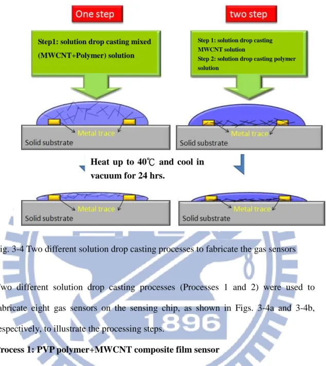
3.6 Preparation of MWCNT-polymer gas sensor-array chip... 37
3.7 Gas sensing experiment ... 43
3.8 Analysis of gas sensing response curve ... 46
Chapter 4 Results and Discussion – comparison between PVP+CNT Composite and Stacked Sensors ...48
4.1. Morphology and structure of MWCNT raw materials ... 48
4.2. Performance of composite and stacked MWCNT - assisted sensors... 50
4.3. Effect of polymer layer thickness on performance of PVP/ MWCNT stacked sensors ... 54
Chapter 5 Results and discussion – polymer/CNT stacked sensors ...57
5.1. Sensing response of six toxic industrial gases... 57
5.2. Sensing response of three chemical warfare agents ... 72
5.3. Sensing response of four liquor gases... 77
5.4. Gas specificity by mathematical PCA analysis on sensing data ... 85
5.5. Performance of sensing chip installed on a portable E-Nose system .... 88
Chapter 6 Conclusions ...91
Chapter 7 Future outlooks ...93
References...95
List of Symbols
A Cross section area of a diffusion tube in gas generator ACN Acetonitrile (solvent)
C Concentration of testing gas
CNT Carbon nanotube
CCl4 Carbon tetrachloride (solvent)
CHCl3 Chloroform (solvent)
CVD Chemical vapour deposition
d Inter-electrode spacing
d plane spacing of a crystal lattice
D Diffusion coefficient
D-band Disorder-induced feature in Raman spectra
dc-PECVD Direct current plasma-enhanced chemical vapour deposition
DCM Dichloromethane (solvent)
DMMP Dimethyl- methyl phosphonate (solvent) ∆R/Rb Electrical resistance ratio
E Electric field
EDX Energy dispersive X-ray spectroscopy ECR Electron cyclotron resonance
Fc Total flow rate of the gas mixture
FESEM Field-emission scanning electron microscopy FET Field effect transistor
E-Nose Electronic nose (system)
G-band Tangential mode in Raman spectra GPIB General-purpose interface bus
HPMC Hydroxypropyl methyl cellulose (polymer) HRTEM High-resolution transmission electron microscopy
IG/ID The G-band and D-band intensity ratio of a Raman spectrum
LSER Linear salvation energy relationship
k-NN k-nearest neighbor method (classification algorithm)
MFC Mass flow controller
MEK Methyl-ethyl ketone (solvent)
MOSFET Metal-oxide-semiconductor field effect transistor MPCVD Microwave plasma chemical vapour deposition
Mw Molecular weight
PCA Principal component analysis method (classification algorithm) PEA Poly(ethylene adipate) (polymer)
PMS Poly(alpha-methylstyrene) (polymer)
PMVEMA Poly(methyl vinyl ether-alt-maleic acid) (polymer) PVBC Poly(vinyl benzyl chloride) (polymer)
P(VDC-AN) Poly(vinylidene chloride-co-acrylonitrile) (polymer) PVP Polyvinylpyrrolidone (polymer)
P Partial pressure of solvent
R Diffusion rate
Rb Resistance of a gas sensor exposing in air
Rmax Resistance peak value of a gas sensor exposing in a tested gas
SEM Scanning electron microscopy SWCNT Singal-walled carbon nanotube SAA Styrene Allyl Alcohol copolymer TEM Transmission electron microscopy
THF Tetrahydrofuran
XSEM Cross sectional SEM micrograph
Table Captions
Chapter 3
Table 3- 1 Raw materials, including chemicals, used in this work... 32 Table 3- 2 Sensing polymer materials selected in this work... 40
Chapter 4
Table 4- 1 Specimen designations of the MWCNTs+PVP composite and the PVP/MWCNT stacked sensors prepared by solution drop method, their
fabrication, sensing conditions, and performance at room temperature. ... 57
Chapter 5
Table 5- 1 Specimen designations of polymer/MWCNT stacked sensor prepared by solution drop method, their sensing conditions, and performance at room
Figure Captions
Chapter 2
Fig. 2- 1 Schematic drawings of (a) Chiral-type, (b) Armchair, and (c) Zigzag CNTs (Lau
and Hui 2002)
. ... 4
Fig. 2-2 (a) The unrolled honeycomb lattice of a nanotube and (b) (4, 2) SWCNT, showing the translation vector T (Dresselhaus et al. 2005b). ... 5
Fig. 2-3 Schematic diagram of arc-discharge system (Saito et al. 1996). ... 7
Fig. 2-4 Schematic of the laser ablation system (Guo et al. 1995). ... 8
Fig. 2- 5 Schematic illustration of the thermal CVD system (Lee et al. 2001). ... 10
Fig. 2- 6 A dc-PE-CVD reactor for the fabrications of CNTs and nanofibers (Chen 2005). ... 10
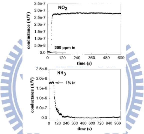
Fig. 2- 7 Conductance change of the CNTs FET sensor when exposed to (a) NO2 and (b) NH3 gases (Kong et al. 2000)... 18
Fig. 2-8 SEM image of prepatterned platinum contacts in resistor geometry (Valentini et al. 2004) ... 19
Fig. 2-9 Time-dependence change of the CNTs’ resistance at an operating temperature of 165 °C and NO2 concentrations ranging from 10 to 100 ppb (Valentini et al. 2004). 20 Fig. 2-10 The measured relative capacitance change of a SWCNT chemicapacitor in response to repeated 20 s pulses of dimethyl formamide (DMF) at varying concentrations (Snow et al. 2005)... 21
Fig. 2-11 (a) Schematic diagram of the nanotube sensor device; (b) diagram of actual test set-up; (c) SEM micrograph of vertically aligned MWCNT film used as the anode (Modi et al. 2003)... 22
Fig. 2-12 Response profile obtained for all analytes by MWCNT/Nylon-6 nanofibers at room temperature: (a) trichloromethane, (b) THF (c) EA, (d) ethanol, (e) acetone, (f) DCM (Lala et al. 2009). ... 23
Fig. 2- 13 Response of CNT/PMMA composite thin film sensor to different dichloromethane vapor concentration (Yoon et al. 2006)... 24
Fig. 2-14 (a) Pictures for the E-Nose system realized by using PDA as personal digital apparatus (b) the identification of tested liquor sample when Hennessy and Johnny Walker are used as test sample (Kim et al. 2005). ... 27
Fig. 2-15 The artificial mucosa comprises multiple chemical sensors distributed along the length of a gas chromatograph channel (Gardner and Covington 2007)... 29
Chapter 3
Fig. 3-1 Flow chart of the experiments. ... 31Fig. 3-2 Schematic diagram of the thermal CVD system. ... 33 Fig. 3-3 Gas testing stand with a sensing chip... 37 Fig. 3-4 Two different solution drop casting processes to fabricate the gas sensors ... 41 Fig. 3-5 Gas sensing experimental setup ... 43 Fig. 3- 6 Typical gas sensing response of a chemiresister sensor (Arshak et al. 2004)... 46
Chapter 4
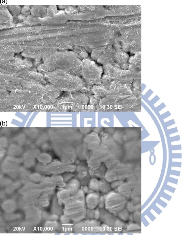
Fig. 4-1 XSEM micrograph of the as-grown MWCNTs... 49 Fig. 4-2 TEM image of a scratched MWCNT tube ... 49 Fig. 4-3 Raman spectrum of the as-grown MWCNTs. ... 50 Fig. 4-4 SEM surface morphologies of: (a) MWCNTs+PVP composite, and (b) the
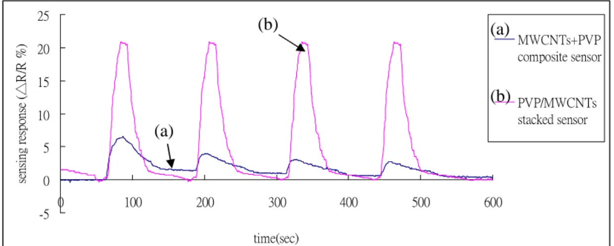
PVP/MWCNTs stacked sensors, respectively ... 51 Fig. 4-5 Typical cycle sensing response (△R/R %) curves of a gas sensor to methanol
gas: (a) for MWCNTs+PVP composite sensor, and (b) for PVP/MWCNTs stacked sensor, respectively. ... 52 Fig. 4-7: Effect of polymer concentration in MEK solution for drop casting on cycle
sensing response (△R/R %) curves of PVP/MWCNTs stacked sensor to methanol gas ... 55
Chapter 5
Fig. 5-1 Effect of gas type and concentration on cycle sensing response (△R/R %) curves for SAA/MWCNTs stacked sensors: (a) THF and (b) CHCl3 gases,
respectively. ... 59 Fig. 5-2 Effect of gas type and concentration on cycle sensing response (△R/R %)
curves for PMVEMA/MWCNTs stacked sensors: (a) MEK, (b) THF, and (c) toluene... 61 Fig. 5-3 Effect of gas type and concentration on cycle sensing response (△R/R %)
curves for PMVEMA/MWCNTs stacked sensors: (a) xylene, (b) CHCl3, and (c)
CCl4... 62
Fig. 5-4 Effect of gas type and concentration on cycle sensing response (△R/R %) curves for PMS/MWCNTs stacked sensors: (a) MEK, (b) THF, and (c) toluene64 Fig. 5-5 Effect of gas type and concentration on cycle sensing response (△R/R %)
curves for PMS/MWCNTs stacked sensors: (a) xylene, (b) CHCl3, and (c) CCl4
... 65 Fig. 5-6: Bar charts of the peak sensing response, (△R/R)max, of the sensing chip under
different gas concentrations for (a) MEK, and (b) THF gases, respectively. ... 67 Fig. 5-7: Bar charts of the peak sensing response, (△R/R)max, of the sensing chip under
Fig. 5-8: Bar charts of the peak sensing response, (△R/R)max, of the sensing chip under
different gas concentrations for (a) CHCl3, and (b) CCl4 gases, respectively. .... 69
Fig. 5-9: Radar plots of the peak sensing response, (△R/R)max), of the sensing chip
under different gas concentrations for (a) MEK, and (b) THF gases, respectively. ... 70 Fig. 5-10: Radar plots of the peak sensing response, (△R/R)max, of the sensing chip
under different gas concentrations for (a) toluene, and (b) xylene gases,
respectively. ... 71 Fig. 5-11: Radar plots of the peak sensing response, (△R/R)max), of the sensing chip
under different gas concentrations for (a) CHCl3, and (b) CCl4 gases, respectively.
... 72 Fig. 5-12 Bar charts of the peak sensing response, (△R/R)max, of the sensing chip to
DMMP gas, respectively. ... 73 Fig. 5-13 Radar plot of of the peak sensing response, (△R/R)max, of the sensing chip to
DMMP gas, respectively. ... 73 Fig. 5-14 Bar chart of the peak sensing response, (△R/R)max, of the sensing chip to
DCM gas, respectively. ... 74 Fig. 5-15 Radar plot of the peak sensing response, (△R/R)max, of the sensing chip to
DCM gas, respectively. ... 74 Fig. 5-16 Bar chart of of the peak sensing response, (△R/R)max, of the sensing chip to
ACN gas, respectively... 75 Fig. 5-17 Radar plot of the peak sensing response, (△R/R)max, of the sensing chip to
ACN gas, respectively... 75 Fig. 5-18 : Bar chart of the peak sensing response, (△R/R)max), of the sensing chip
under different gas concentrations for (a) Japanese sake, and (b) Kin-men sorghum gases, respectively. ... 77 Fig. 5-19 : Bar chart of the peak sensing response, (△R/R)max), of the sensing chip
under different gas concentrations for (a) medical liquor, and (b) Scotch whisky gases, respectively. ... 78 Fig. 5-20: Radar plots of the peak sensing response, (△R/R)max), of the sensing chip
under different gas concentrations for (a) Japanese sake, and (b) Kin-men sorghum gases, respectively. ... 79 Fig. 5-21: Radar plots of the peak sensing response, (△R/R)max), of the sensing chip
under different gas concentrations for (a) medical liquor, and (b) Scotch whisky gases, respectively. ... 80 Fig. 5-22 : Bar chart of the peak sensing response, (△R/R)max), of the sensing chip
under different gas concentrations to methanol gases, respectively. 錯誤錯誤錯誤! 尚未定錯誤 尚未定尚未定尚未定 義
義 義
Fig. 5-23: Radar plots of the peak sensing response, (△R/R)max), of the sensing chip
under different gas concentrations to methanol gases, respectively. 錯誤錯誤錯誤! 尚未定錯誤 尚未定尚未定尚未定 義書籤
義書籤 義書籤 義書籤。。。。
Fig. 5-24 The 2-D PCA plot for sensing responses of eight sensors on a chip to three different gas types (i.e. ACN, DCM and DMMP gases) ... 86 Fig. 5-25 The 3-D PCA plot for sensing responses of eight sensors on a chip to six
different gas types (i.e. MEK, THF, toluene, xylene, CHCl3, and CCl4 gases) ... 86
Fig. 5-26 The 3-D PCA plot for sensing responses of eight sensors on a chip to five different gas types (i.e. Japanese sake, Kin men sorghum, medicinal liquor, Scotch whisky and methanol gases) ... 87 Fig. 5-27: Optical pictures of a portable E-Nose system: (a) the whole equipment, and
(b) its control panel. (P = power On/Off, I = system initialization, S =
training/testing mode selection, E = enter) ... 89
Chapter 1
Introduction
Carbon nanostructured materials have attracted considerable research attentions in the past few decades due to their unique physical properties, such as high specific surface area, good corrosion resistance, tailorable pore size, and excellent electronic conductivity. These properties make carbon nanostructured materials suitable for applications as electrodes or as supports for electrode catalysts. For gas sensing applications, CNT-derived high-sensitivity gas sensors for various gases and nerve agents, such as ammonia, ethanol vapor, NO2, CO, CH4, and dimethyl
methylphosphonate (DMMP) have been reported (Li et al. 2003; Snow et al. 2005; Someya et al. 2003). In recent years, the various E-Nose (electronic nose) systems(Bartlett et al. 1993; Craven et al.
1996; Gardner 2004; Gardner and Bartlett 1994; Pearce et al. 2003)
, designing in an effort to microminiaturize the size, were developed to cut down the prices, to offer higher gas sensitivity and higher gas specificity. The sensing materials used for chemical resistors could be divided into two major types: inorganic semiconductors (Gopel and
Schierbaum 1995; Meixner et al. 1995)
and organic polymers (Gardner and Bartlett 1995; Lonergan et al. 1996; Slater
et al. 1993)
. The sensing material is essentially to trigger physical reactions with the adsorptive analytes and then to change its resistivity or dielectric constant. The concentration of the analytes can be determined from the amount of property variation. The sensing polymer materials were generally fabricated in the form of thin films, which might provide the following advantages (Doleman et al. 1998; Ryan and Lewis 2001; Severin et al.
2000)
. In addition to be readily coupled to microstructure sensor(Hagleitner et al. 2001), the thin film sensors can enhance the gas adsorption and desorption abilities to improve the gas sensitivity and the quick repeating use, respectively.
In this study, MWCNTs and conducting polymers, which used in the chips, were selected according to their linear salvation energy relationship (LSER) and physical absorption bonding properties (Kim et al. 2005; Wang et al. 2010). These polymer/CNTs stacked sensors are simple to operate and the sensing film quality can be easily controlled through the solution drop casting process. By using the well-controlled gas sensing experiments, the different sensing behaviors of the MWCNT-assisted polymer stacked sensors in the array can be determined.
By collating data, based on different resistance to volume variations of each sensor in the gas sensing array under different gases and concentrations, and summarized the cases in the response bar chart, or called “the radar plots”, the selected chemical gas sensing materials library can be established. In other words, the gas specificity can be enhanced by selecting polymer sensing materials with different sensing responses to different gases to form different patterns of the radar plots. By using the method of principle component analysis (PCA) on a PC, or the k-nearest neighbor (k-NN) classification algorithm on the portable system, the analyzing works to determine the gas specificity and concentration can be simplified, and the feasibility has been demonstrated with electronic nose (E-Nose) system. The analytes include three simulants of chemical warfare agents, six toxic industrial compound gas, four commercial liquors and methanol.
Chapter 2
Literature reviews
2.1
Carbon nanostructured materials
Carbon is the fourth most abundant chemical in the universe (by mass). Due to its unique electron structure, it readily forms covalent bonds with itself and other elements. Thus carbon is chemically one of the most flexible elements known to man, as seen in the contrast between diamonds (the hardest material discovered) and graphite (one of the softest materials). Carbon may form a variety of crystals, amorphous and nanostructured materials with extremely different properties. Carbon nanotubes (CNTs) and fullerenes are two of the most attractive nanostructured materials due to their unique electronic, mechanical, optical, and chemical properties(Dekker 1999). Carbon nanostructured materials have been reported a broad range of applications in the fields of molecular electronics(Avouris 2002), sensing materials(Wang 2004), nano- and micro electromechanic devices(Tombler et al. 2000), field-emission display materials (Choi et al. 1999), energy storage(Che et al. 1998), and composite materials(Moniruzzaman and Winey 2006).
2.1.1 Structure and property of Carbon nanotubes
CNTs, which are formed by rolling the graphene sheets, were first discovered by Iijima in 1991(Iijima 1991). In early twentieth century, it becomes one of the most exciting new materials in the field of nanoscience and nanotechnology. Various forms of CNTs have been developed over the past few decades by different fabrication
approaches. There are different ways of classification of CNTs. Based on number of graphene layers of tube wall(Pillai et al. 2007; Saito et al. 2004), they are called single-, double- or multi-walled CNTs(Bethune et al. 1993; Iijima and Ichihashi 1993; Wei et al. 2003). In other words, a single-walled carbon nanotube (SWCNT) can be described as a layer of hexagonal graphene sheet rolled into a seamless cylinder, whilst a multi-walled carbon nanotube (MWCNT) is formed with multiple graphene layers. CNTs also could be classified by tube morphology (bamboo-like/hollow, or helix/straight) (Amelinckx et al. 1994), cap morphology (close/open) (Pan et al. 1999), growth mode (tip-/base-growth) (Abdi et al. 2006;
Bower et al. 2000; Chen et al. 2004; Chen et al. 2000; Choi et al. 2002; Choi et al. 2001; Dupuis 2005; Fan et al. 1999; Gulino et
al. 2005; Hart et al. 2006; Hsu et al. 2002; Kuo et al. 2003; Lee et al. 1999; Lee et al. 2001; Lee and Park 2000; Lee et al. 2004;
Lin et al. 2003b; Melechko et al. 2002; Murakami et al. 2000; Ren et al. 1998; Yap et al. 2006; Zhao et al. 2006)
, or crystal structures (zigzag/chiral/armchair, as shown in Fig. 2-1)(Ge and Sattler 1994; Saito et al. 1992).
Fig. 2- 1 Schematic drawings of (a) Chiral-type, (b) Armchair, and (c) Zigzag CNTs
(Lau and Hui 2002)
.
These three structural arrangements may be classified as non-chiral and chiral structural types, depending on their rolling direction(Saito et al. 2004) For non-chiral structure of SWCNTs, the honey comb lattices of the nanotube are parallel to the tube axis, which can further be classified as armchair (Fig. 2- 1b) and zigzag (Fig. 2- 1c) arrangements (Saito et al. 1992). For the armchair structure, two C-C bonds on opposite
sides of each hexagonal lattice are perpendicular to nanotube axis, whereas for the zig-zag structure, the bonds are parallel to nanotube axis. Unlike non-chiral structures, the C-C bonds in chiral structures (Fig. 2- 1a) are with an angle to the nanotube axis.
Fig. 2-2 (a) The unrolled honeycomb lattice of a nanotube and (b) (4, 2) SWCNT, showing the translation vector T (Dresselhaus et al. 2005b).
Formation of CNT from a grapheme sheet was analyzed mathematically by Fig.2-2. When sites O and A, and B and B’ in Fig. 2-2 are connected, a portion of a graphene sheet can thus be rolled seamlessly to form a SWCNT. Meanwhile, vectors OA and OB are defined as the chiral vector, Ch, and the translational vector T of the
nanotube. This rectangle portion, OAB’B, is then defined as a unit cell of the nanotube. Generally, a SWCNT is mathematically specified by a chiral vector, Ch,
(Fig. 2-2a), given by the following equation (Dresselhaus et al. 2005b; Saito et al. 2004): ) , ( 2 1 na n m na Ch = + ≡ (Eq. 2-1)
Where a1 and a2 are unit vectors of the two-dimensional (2D) hexagonal lattice, n and
for example, with a chiral vector Ch = (n, m) = (4, 2), the nanotube in Fig. 2-2 is
described as a (4, 2) SWCNT.
The electrical properties of CNTs can either be metallic or semiconducting, depending on their tube diameter and chirality. Nanotubes with n-m = 0 are metallic while all the others are semiconducting. In terms of mechanical properties, CNTs normally exhibit a Young's modulus of 0.8~5.0 TPa and a tensile strength of 10~150 GPa owing to the presence of C-C bonds. They are among the strongest and stiffest fibers known to date. Thermally, CNTs have a high thermal stability both under vacuum and air and an excellent thermal conductivity as high as ca. 3500 W/ (m·K), which is five times higher than copper at room temperature.
2.1.2 Synthesis methods of CNTs (a) Arc-discharge method
CNTs were first synthesized by arc-discharge method, as reported by Iijima and co-workers in 1991 (Iijima 1991). Fig. 2-3 shows(Satio 1995) the schematic drawing of the arc-discharge system, in which two graphite rods are used as anode and cathode electrodes, respectively.
Fig. 2-3 Schematic diagram of arc-discharge system (Saito et al. 1996).
The discharge system is normally operated at a voltage ranging from 20 to 40 V and a current from 40 to 100 Ampere under either He or Ar gas pressure of ca. 10~500 Torr. Carbon clusters emerging from the anodic graphite rod via electron bombardment may be deposited on the cathode surface. These carbon products may include amorphous carbon, fullerenes, carbon cluster, carbon nanotubes, and other carbon structures. During the CNT production process, arcing occurs when DC voltage is applied between these two electrodes. By incorporating a desirable amount of metallic catalysts, such as Fe, Co, Ni, and Y, SWCNTs are formed at the anode
(Bethune et al. 1993)
, while MWCNTs can be fabricated by using pure graphite at both electrodes. Therefore, post treatment is often required to purify the nanostructures for practical applications. In addition, the drawback of this method is its low yield in CNTs.
(b)Laser ablation
Laser ablation was first reported by Guo and co-worker in 1995(Guo et al. 1995), as illustrated in Fig. 2-4. An incident laser beam is applied to vaporize a graphite target under helium or argon gas atmosphere at a pressure of 500 Torr. The products are swept out by the flowing gas and eventually deposited on the water cooled collector. As such, it is also named as the laser vaporization method. The graphite target used in this scheme often contains a small amount of Co, Ni, Fe, or Y as catalyst, SWCNTs grow very fast from atoms and molecules within these first few milliseconds, the majority of growth appears to occur from a feedstock of mixed nanoparticles over seconds of annealing time. (Puretzky et al. 2000).
(c) Chemical vapor deposition
Chemical vapor deposition (CVD) method has been known to be a mature technique in thin film processing. A variety of different films can be fabricated by CVD method, covering from metals, semiconductors to insulators. By using the CVD method, arrays of CNTs can be produced through decomposition of carbon-containing gaseous species (such as CH4(Dai 2002), C2H2(Wang et al. 2001), C2H4(Cheung et al. 2002), C6H6(Yang et al. 2003)
, CO(Dai et al. 1996), etc.) on various substrates containing transition metal catalysts. During the CVD process, it is essential to introduce some forms of energy to decompose the precursor gases and to deposit the reaction product on the substrate surface. The energy introduced may be thermal, microwave, RF power, or other forms of energy, thus, leading to different process names for the production of CNTs. For examples, microwave plasma enhanced CVD (MPE-CVD)(Lin et al. 2003a) , electron cyclotron resonance CVD (ECR-CVD) (Kuo et al. 2003), inductively coupled plasma CVD (ICP-CVD) (Delzeit et al. 2002), RF plasma enhanced CVD (rf-PE-CVD) (Kato et al. 2004), DC plasma enhanced CVD (dc-PE-CVD) (Hofmann et al. 2007b), thermal CVD(Lee and Park 2000), hot filament CVD (HF-CVD) (Yang et al. 2004), etc. In general, these CVD systems can be roughly classified as thermal and plasma CVD on the basis of their working principles. Typically, the former process includes a substrate preheating zone and CNTs are grown while the precursor gases are flowing through the catalyst/substrate (shown in Fig. 2- 5). The heat source of plasma CVD mainly arising from the plasma, as illustrated by a dc-PE-CVD system in Fig. 2- 6. Compared with arc-discharge and laser ablation methods, CVD enhanced by plasma is more economical (lower reaction temperature) and the reaction process can also be controlled more easily. Moreover, it is superior compared to other methods in terms of the purity, yield, and controlled alignment of the CNT products. Recent advancements in plasma enhanced CVD have been focusing on the development and fabrication of vertically aligned CNTs.
Fig. 2- 5 Schematic illustration of the thermal CVD system (Lee et al. 2001).
2.2
Structure analyses and property measurements
The principles of typical microstructure examination techniques and Raman spectroscopy property measurement commonly used for characterization of porous and nano carbon materials are summarized below:
2.2.1 Scanning electron microscopy (SEM)
Generally, a scanning electron microscope (SEM) is a type of electron microscope that produces images of a sample by scanning over it with a focused beam of electrons. The electrons interact with electrons in the sample, producing various signals that can be detected and that contain information about the sample's surface topography and composition. The SEM apparatus is consists of an electron gun, which serves to generate electron beams that, in turns, are accelerated under high voltage (0.4-40 keV). SEM can achieve resolution better than 1 nanometer. By deflecting the incident beams with the focusing coils, a two-dimensional image can be obtained by detecting the reflected secondary and backscattered electrons.
All samples must also be of an appropriate size to fit in the specimen chamber and are generally mounted rigidly on a specimen holder called a specimen stub. Several models of SEM can examine any part of a 6-inch (15 cm) semiconductor wafer, and some can tilt an object of that size to 45°. The SEM was often being employed to observe the growth behaviors of carbon nanotubes on the substrates.
2.2.2 Transmission electron microscopy (TEM)
Transmission electron microscopy (TEM) is a microscopy technique where a beam of electrons is transmitted through an ultra thin specimen, interacting with the
specimen as it passes through. An image is formed from the interaction of the electrons transmitted through the specimen; the image is magnified and focused onto an imaging device, such as the fluorescent screen, or to be detected by a CCD camera sensor. Transmission electron microscopy is the most important technique for studying microstructure of materials in great detail. Typically, an electron beam with accelerating voltage of 100-400 keV would illuminate a region of the specimen. The transmitted and diffracted electrons are recombined by the objective lens to form a diffraction pattern in the back focal plane of that lens and a magnified image of the sample in its image plane. A number of intermediate lenses are used to project either the image or the diffraction pattern onto a fluorescent screen for observation. The screen is usually lifted and the image may be printed out on photographic film or stored for recording purposes.
The methods for TEM sample preparation from carbon deposit can be categorized into some main groups: (1) Ultrasonic method, but this carbon nanotube (CNT) preparation method disenables to determine the growth mode and may lead to the structural damage and removal of catalysts from CNTs(Park et al. 2002). (2) Ion thinning technique, the cutting and ion thinning techniques preserve the CNT structure and enable unambiguous determination of the CNT ends, as well as evaluation of interfacial structure of CNTs –catalyst – substrate(Zhang et al. 2001).
Some researchers also used this instrument to observe dynamic effects before and during catalyst-assisted CVD of CNFs and SWCNTs(Hofmann et al. 2007a). And they also found data of various stages of SWCNT growth. The TEM images also show the catalyst crystals for which SWCNT nucleation has stopped early. A small-sized carbon cap has emerged on top of each catalyst particle. The carbon network surrounding the deactivated catalyst particle forces a stronger faceting.
2.2.3 Raman spectroscopy
Raman spectroscopy is a spectroscopic technique used to study vibrational, rotational, and other low-frequency modes of the materials in a system. Normally, a monochromatic laser beam is used as the incident light source, upon irradiating on the substrate, photons may be absorbed, scattered, or not interacting with the sample. When the light is elastically scattered from an atom or molecule, the scattered photons have almost the same frequency with the incident photons. However, a small fraction of the light may be scattered during excitation, such scattered photons would have a frequency different from, and usually lower than, the frequency of the incident photons. As such, the energy difference between the monochromatic light and the Raman scattered light should be equal to the energy involved in changing the molecule’s vibration state (Dresselhaus et al. 2002; Dresselhaus et al. 2005a; Jorio et al. 2003). This energy difference is called the Raman shift. Typically several different Raman signals may often be observed; each being associated with different vibration or rotational motions of molecules in the sample.
Typically, Raman spectroscopy is also a popular technique for determining the diameter distribution, chirality, purity, and architecture of CNTs(Dresselhaus et al. 2002). The most prominent Raman features in CNTs are the radial breathing modes (RBMs), the higher frequency D (disordered), G (graphite), and G' (second-order Raman scattering from D-band variation) modes. The RBM mode is a confirmation for the presence of SWCNTs in a sample, since it is not present in graphite. This mode is located between 75 and 300 cm-1 from the excitation line, and is associated with the symmetric movement of carbon atoms in the radial direction. The RBM frequency is inversely proportional to the nanotube diameter with the relationship:
ωr (cm-1
) = 224 (cm-1) /dt (nm) (Eq. 2-2)
Tube diameters between 0.8 and 1.3 nm give nearly identical results. Most single-grating Raman spectrometers have cutoff frequencies between 100 and 120 cm-1, which restricts the range of tube diameters smaller than 2 to 2.5 nm. The D band, which normally locates at ca. 1300 cm−1 is associated with carbons with the sp3 structures, such as functionalized and amorphous carbons, whereas the G band locates at ca. 1600 cm−1 is normally assigned to carbons with the sp2 structure carbon, such as graphite. The G'-band frequency is close to twice that of the D band and is found from 2500 to 2900 cm-1. The G' band is an intrinsic property of the nanotube and graphite, and present even in defect-free nanotubes for which the D band is completely absent.
2.3
Gas sensing devices and their working principles
A sensor is a device that measures a physical quantity and converts it into a signal which can be read by an observer or by an instrument. The sensor's sensitivity indicates how much the sensor's output changes when the measured quantity changes. The sensors sorted by type list in the follow: (1) acoustic (2) biological (3) chemical (4) electric (5) magnetic (6) mechanical (7) optical (8) radiation (9) thermal, etc.[ref]
This research will focous on the chemical gas sensor, and will illustrate some of these chemical gas sensors with carbon nanotubes as the sensing materials. The chemical gas sensor contains two or three electrodes, occasionally four, in contact with an electrolyte. The gas diffuses into the sensor, through the back of the porous membrane to the working electrode where it is oxidized or reduced. These sensors features advantages such as compact, light weight, easy to be carried, cheap price, robust and capable of real-time monitoring thus it becomes the research subject for institutes all over the world.
Among all gas sensors, the most representative one is “chemiresistors”(Gardner and
Bartlett 1993)
. The operating principle of chemiresistor is based on the variation of resistance when a conductive polymer electrode is exposed in chemical gases. The polymer is coated on the circuit board and it will absorb chemical gas and cause swelling of polymer after exposure. This swelling of polymer will then vary the electrode resistance. The specific resistance variation can be used as signal to estimate the concentration of tested gas. The key to the fabrication of “chemiresistor” is selection of polymer material. There are two major types:(1) Chemiresistor made of ICP (Intrinsically Conducting Polymers), utilizing the semiconductor property of conductive polymer. For the past ten years, this type of sensors was mostly applied to
the sensing of chemical and bio-chemical substances. (2) Chemiresistor made of composite material by mixing conductive substances with non-conductive polymers, called LP (i.e. loaded polymers). The conductive substances here are mainly carbon black mixing with inorganic semiconductor or metal powder. The studies on composite sensor array fabricated by mixing different polymers with conductive carbon black were broadly conducted by Lewis(Albert et al. 2000) and the others (Collins et al.
2000; Dekker 1999; Derycke et al. 2002; Postma et al. 2001; Romero et al. 2002; Rosenblatt et al. 2002)
for gas specificity applications.
2.4
Carbon nanostructure-based gas sensing devices
Carbon nanotubes (CNTs) are molecular scale quantum wires exhibiting many unique properties for potential nano-devices applications (Chopra et al. 2002; Snow et al. 2003;
Snow et al. 2005; Someya et al. 2003)
. One of the applications is to act as the gas sensing materials due to its high specific surface area to enhance the gas sensitivity. They also possess high thermal stability to increase possibility to be deployed in most environments. Depending on the types of sensing signals, these devices can be classified into four types, including sensing gas ionization, capacitance, and resistance and field effect changes, as described in the following sections.
2.4.1 Semiconducting CNTs FET Gas Sensors
As addressed in the previous section, SWCNTs can be either semiconducting or metallic. If two metal contacts are connected to each end of an individual semiconducting SWCNT (S-SWCNT), the metal/S-SWCNT/metal device exhibits p-type transistor characteristics. Therefore, the resistance response of CNTs to gas adsorption can be detected with field effect transistors (FETs) by Kong et al (Kong et al.
2000)
. Figure 2-7 shows the conductance versus time curves of the transistor upon exposure to NO2 and NH3 at room temperature. A sharp increase in conductance of
the S-SWCNT FET by about three orders of magnitude was observed after introducing 200 ppm of NO2 into the testing chamber (Figure 2-7(a)). The response
time was about 2–10 seconds, and the sensitivity (the ratio between resistance after and before gas exposure) was about 100 to 1000. Exposure to NH3 effectively shifts
depletion and reduced conductance. For the NO2 case, exposure of the initially
depleted sample to NO2 resulted in the nanotube Fermi level shifting closer to the
valence band. This caused enriched hole carriers in the nanotube and enhanced sample conductance.
Fig. 2- 7 Conductance change of the CNTs FET sensor when exposed to (a) NO2 and
(b) NH3 gases (Kong et al. 2000)
2.4.2 CNTs-Based Resistor Gas Sensors
The resistance change of CNTs under gas exposure can also be detected by resistors with dc voltage. Valentiniet et al (Valentini et al. 2004) designed a CNT serpentine resistor for the detection of various gases including NO2, CO, NH3, H2O, and C2H5OH.
and then CNTs films were grown on the substrate by using radiofrequency plasma enhanced CVD (RF-PECVD) with Ni as the catalyst. Figures 2-8 shows the as-grown CNTs and a scheme of the sensor design.
Fig. 2-8 SEM image of prepatterned platinum contacts in resistor geometry (Valentini et al.
2004)
The sensor showed a good sensitivity to NO2 at room temperature. However, at
165℃, the sensor showed the best response as a tradeoff between the higher resistance variations and the fast and reproducible baseline recovery. The dynamic gas response of CNT films at an operating temperature of 165 °C and NO2 concentrations
ranging from 10 to 100 ppb. From Fig. 2-9 the amazing result is that the CNT film is sensitive to NO2 at concentrations as low as 10 ppb and that when the NO2
concentration is increased and decreased stepwise in this range, the sensor response is reproducible and stable. In order to explain the obtained results, the chemical nature of the NO2 molecule has to be considered. Recent experimental results refer to the
electrical conductance of an individual semiconducting single-walled tube strongly increasing upon NO2 gas exposure and that the NO2 is identified as an electron
acceptor. A possible interpretation of the electrical response of CNT films to NO2 gas
could be the physical absorption of this molecule. NO2 has an unpaired electron and is
known as a strong oxidizer. Upon NO2 adsorption, a charge transfer is likely to occur
from CNTs to NO2 due to the electron–acceptor character of NO2 molecules.
Fig. 2-9 Time-dependence change of the CNTs’ resistance at an operating temperature of 165 °C and NO2 concentrations ranging from 10 to 100 ppb (Valentini et al. 2004)
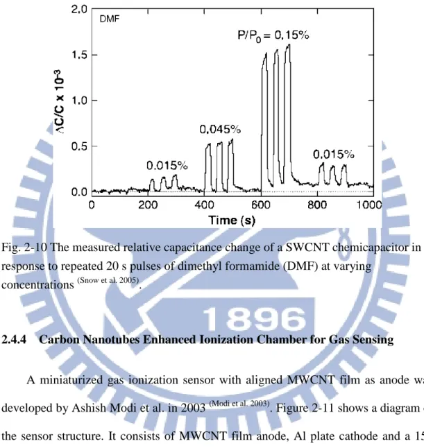
2.4.3 CNTs-Based capacitance Gas Sensors
Snow et al demonstrated the use of SWCNTs as chemicapacitors for sensing of both polar and non-polar gas molecules at room temperature (Snow et al. 2005). The SWCNT-based chemicapacitors were fabricated by a CVD-grown SWCNT network on a 250 nm thick thermally grown silicon oxide on a highly doped silicon substrate. The capacitance was measured at 30 kHz and 0.1 VAC bias between the SWCNTs and
the heavily doped silicon substrate with 250 nm thick SiO2. Under the applied bias,
strong fringing electric fields radiate outward from the SWCNTs surface and the polarization of the adsorbates can be detected as an increase in capacitance. This
capacitance change was fast (< 4 s response time), sensitive, completely reversible, and with low electrical noise. This approach enables detection of a wide range of analytes including less polar chemical vapors such as dimethyl formamide (DMF) and DMMP (figure 2-10).
Fig. 2-10 The measured relative capacitance change of a SWCNT chemicapacitor in response to repeated 20 s pulses of dimethyl formamide (DMF) at varying
concentrations (Snow et al. 2005).
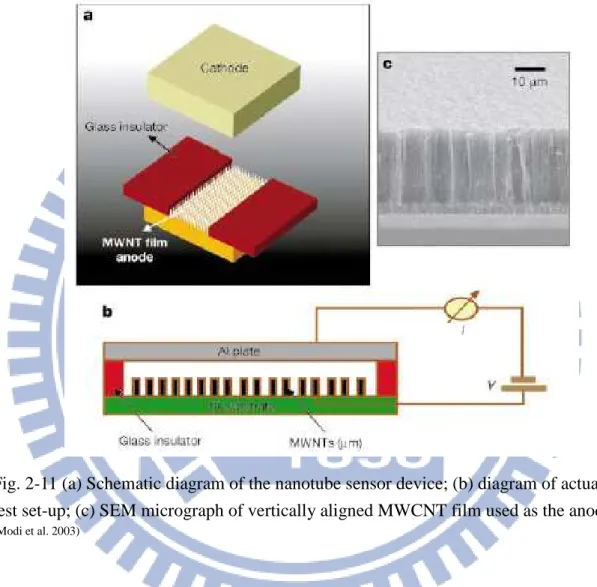
2.4.4 Carbon Nanotubes Enhanced Ionization Chamber for Gas Sensing
A miniaturized gas ionization sensor with aligned MWCNT film as anode was developed by Ashish Modi et al. in 2003 (Modi et al. 2003). Figure 2-11 shows a diagram of the sensor structure. It consists of MWCNT film anode, Al plate cathode and a 150
μm thick glass insulator between them. The vertically aligned MWCNT film was
prepared by CVD on SiO2 substrate with tip diameter in the range of 25 ∼ 30nm and
30 µm in length (Figure 2-11 (c)). This results in the formation of a “corona” or conduction filament of high ionized gas that surrounds the MWNT tips, and thereby promotes the formation of a self-sustaining interelectrode discharge at very low
voltage. Compared with ionization chamber with metal anode (without CNTs), the breakdown voltage of air was brought down dramatically from 960V to 346V. Different gases including NH3, CO2, N2, O2, He, Ar, and air were tested and showed
distinct and precise breakdown voltage.
Fig. 2-11 (a) Schematic diagram of the nanotube sensor device; (b) diagram of actual test set-up; (c) SEM micrograph of vertically aligned MWCNT film used as the anode
(Modi et al. 2003)
The single-walled carbon nanotubes (SWCNTs), multi-walled carbon nanotubes (MWCNTs) and randomly oriented nanotube networks for detecting chemical gases and vapors have been a subject of active research (Park et al. 2010) . But slow response and recovery is a challenge to be addressed for CNTs-based gas sensors, which are caused by the nature of nanotubes materials. However, with the increasing interests and development of related technologies, CNTs-based gas sensors have a promising opportunity and will bring a giant change to the current life.
2.5
Carbon nanostructure-assisted gas sensing devices
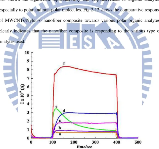
Non-conductive polymers causing the bulk dissolution of gas into the film can bring about changes of their physical properties. The feasibility of using MWCNTs/Nylon-6 nanofiber materials for gas sensing at room temperature has been demonstrated by Neeta L. Lala et al. in 2009 (Lala et al. 2009). The nanofiber based device has shown the significant reproducibility and responsiveness to organic analytes, especially to polar and non-polar molecules. Fig 2-12 shows the comparative response of MWCNTs/Nylon-6 nanofiber composite towards various polar organic analytes, clearly indicates that the nanofiber composite is responding to the various type of analytes used.
Fig. 2-12 Response profile obtained for all analytes by MWCNT/Nylon-6 nanofibers at room temperature: (a) trichloromethane, (b) THF (c) EA, (d) ethanol, (e) acetone, (f) DCM (Lala et al. 2009).
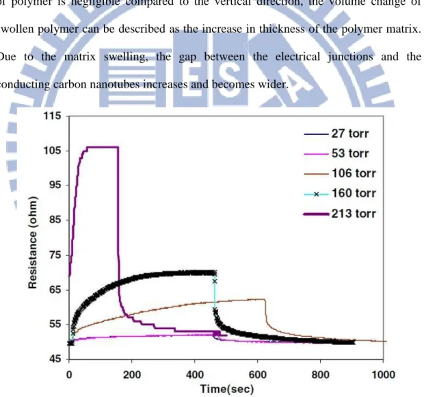
Hargsoon Yoon et al. in 2006 (Yoon et al. 2006) measured the responses of f-CNT/PMMA composite sensors for different gas concentrations by using
conventional resistance measurement methods. As shown in figure 2-13, the resistance of CNT/PMMA composite thin film rapidly increased with dichloromethane vapor concentration. It is observed that the resistance of the composite in figure increased with gas concentration and reached saturated values within 10 min. The resistance increase is regarded as being caused by the free volume change of the PMMA polymer matrix. The volume change is determined by the exposure time and concentration of dichloromethane vapor. Because lateral expansion of polymer is negligible compared to the vertical direction, the volume change of swollen polymer can be described as the increase in thickness of the polymer matrix. Due to the matrix swelling, the gap between the electrical junctions and the conducting carbon nanotubes increases and becomes wider.
Fig. 2- 13 Response of CNT/PMMA composite thin film sensor to different dichloromethane vapor concentration (Yoon et al. 2006)
2.6
Introduction to olfaction
Smell is a primal sense for humans as well as animals. From an evolutionary standpoint it is one of the most ancient of senses. Smell (or Olfaction) allows vertebrates and other organisms with olfactory receptors to identify food, mates, and predators.[ref] Accordingly, it provides both sensual pleasure (the odor of flowers and perfume) as well as warnings of danger (e.g., spoiled food, chemical dangers). For both humans and animals, it is one of the important means by which our environment communicates with. Olfaction is a prime example; the discovery of the gene family encoding vertebrate olfactory receptors (ORs) (Buck and Axel 1991) has led to a relatively detailed understanding of the molecular and neurological bases for how organisms can smell volatile compounds. Linda B. Buck and Richard Axel won the 2004 Nobel Prize in Physiology or Medicine for their work on the study of “Odorant receptors and the organization of the olfactory system”.
The olfactory area of two nasal passages in humans is a small area containing in total approximately 50 million primary sensory receptor cells. The olfactory regions be made of cilia down out of the olfactory epithelium into a 60 microns thick layer of mucous. This mucous layer is a lipid-rich secretion at the epithelium surface. Therefore, they can interact with the olfactory receptors and produce the signals that our brain interprets as odor. Humans have several hundred distinct genes that encode olfactory receptor proteins and rodents have an increase of 500 to 1000 separate genes, that is, as much as 1% of the genome. This extremely broad range of receptor types permits the detection of odor sources comprised of unpredictable mixtures of molecular species, and even allows detection of newly synthesized compounds with unknown functions.
2.7
Artificial electronic nose system
An artificial electronic nose (E-Nose) system is a biomimetic system for odor detection, analysis, and recognition. Since it was first developed in 1987 (Gardner and
Bartlett 1994; Gardner 1987)
, the E-Nose has been adapted in a wide range of applications, such as environmental monitoring (Baby et al. 2000; Lamagna et al. 2008), food product quality control (Balasubramanian et al. 2008; Capone et al. 2000; Panigrahi et al. 2006), agricultural evaluation (Gomez
et al. 2006; Pathange et al. 2006)
, the automotive industry (Morvan et al. 2000; Park et al. 2009; Sobanski et al.
2006)
, health management, and medical diagnosis (Bernabei et al. 2008; D'Amico et al. 2010; Lin et al.
2001; Pavlou et al. 2002)
.
Recent efforts have yielded a miniaturized and inexpensive chemical gas sensor
(Guerin et al. 2005; Tang et al. 2006; Yamaguchi and Yang 2004)
with high reproducibility and a rapid reaction rate. Research, including that from our own group working under size and price restraints, has produced a portable E-Nose based on a carbon black-polymer composite sensor array (Kim et al. 2005; Tang et al. 2010) , shown in fig 2-14.
Fig. 2-14 (a) Pictures for the E-Nose system realized by using PDA as personal digital apparatus (b) the identification of tested liquor sample when Hennessy and Johnny Walker are used as test sample (Kim et al. 2005).
Compared those of with carbon black, the electrical conduction properties of carbon nanotubes (CNTs) have drawn considerable interest (Park et al. 2009), and multiple-walled carbon nanotube (MWCNTs)–polymer composite sensors show very good performance with respect to sensitivity, response time, reproducibility, and long-term stability (Alig et al. 2007; Wu and Lin 2006).
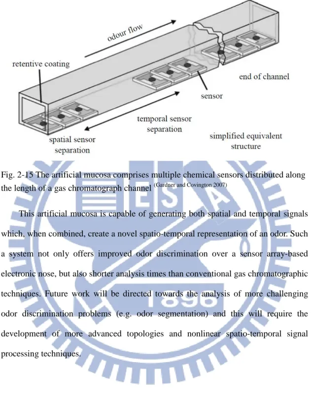
To improve sensor performance further, researchers have studied biological olfaction as a reference. Mammalian olfactory receptor cells distributed in the olfactory epithelium contain a mucous covering layer. The surface of an olfactory cell consists of tens of cilia, which extend into the mucus. As gas molecules enter the nose, they first dissolve in the mucus before being captured by the cilia. The mucus filters out dust and impurities that could otherwise damage the cilia. The receptor cells then transmit neural signals to the cerebrum. This two-layer structure inspired researchers to investigate the use of artificial mucosa to emulate this mechanism, and the use of artificial mucosa as shown in Fig. 2-15, resulted in a five-fold increase in sensitivity
(Gardner and Covington 2007)
. The artificial mucosa approach uses GC columns with a 10 mm thick layer of Parylene C (polymonochloroparaxylylene C) to emulate the mucosa and 40 polymer-composite sensors to emulate the cilia.
Fig. 2-15 The artificial mucosa comprises multiple chemical sensors distributed along the length of a gas chromatograph channel (Gardner and Covington 2007)
This artificial mucosa is capable of generating both spatial and temporal signals which, when combined, create a novel spatio-temporal representation of an odor. Such a system not only offers improved odor discrimination over a sensor array-based electronic nose, but also shorter analysis times than conventional gas chromatographic techniques. Future work will be directed towards the analysis of more challenging odor discrimination problems (e.g. odor segmentation) and this will require the development of more advanced topologies and nonlinear spatio-temporal signal processing techniques.
Chapter 3
Experimental details
3.1
Experimental flow chart
The flow chart for the experiments in this work is shown in Fig. 3-1. In brief, CNTs were prepared by thermal CVD with C2H2 and H2 as source gases, FeCo as
catalyst and MgO as capping layer on catalyst layer. The CNTs were then mixed with sensing polymer materials and drop cast on Si wafer to act as gas sensor. The CNTs were also used as the base layer and followed by drop casting sensing polymer on the top to act as gas sensor. The gas sensing chip with eight different sensors was then installed on a gas testing stand for gas sensing experiments and followed by data analyses with one of two mathematical methods (PCA, k-NN), as will be described in the following text. The structures and properties of as-grown CNTs were characterized by SEM, TEM and Raman spectroscopy.
Si Wafer
SEM, Raman Catalyst deposition
FeCo film
Capping layer deposition MgO film CNTs deposition by Thermal CVD (C2H2 + H2) Lithography process to prepare interdiglal circuit
Install on gas sensing testing stand
Solution drop casting several times (polymer + MEK)
Gas sensing experiment
Sensing Solution preparation (CNTs + surfactant + Polymer)
Data analysis
Remove CNTs from wafer TEM
Sensing Solution preparation by ultrasonic agitation (CNTs + MEK)
Form stacked gas sensor chip Form composite gas sensor chip
Solution drop casting several times Solution drop casting
several times (CNT + MEK)
Install on gas sensing testing stand Lithography process
to prepare interdiglal circuit
3.2
Raw materials
The raw materials used in this work, including wafer, alloy, oxide, gas, chemical, and polymer materials are listed in Table 3-1.
Table 3-1 Raw materials, including chemicals, used in this work
*Material (purpose) Formula Supplier
P-type (100) silicon wafer
(substrate) 99.9999% Tekatarter Co.
Iron Cobalt
(catalyst for CNTs growth) FeCo (99.99%) Tekatarter Co. Magnesium Oxide
(capping layer for CNT growth) MgO (99.99%) Summit-Tech. Co. Acetylene
(source gas for CNT growth) C2H2 (purity 99.9995%) San Fu Argon
(carrier gas for CNT growth) Ar (purity 99.998%) San Fu Hydrogen
(source gas for CNT growth) H2 (purity 99.9995%) San Fu Acetonitrile(ACN) (analyte) CH3CN
(Anhydrous, 99.8%) Sigma-Aldrich Carbon tetrachloride (analyte) CCl4
(Reagent grade, 99.9%) Sigma-Aldrich
Chloroform(analyte) CHCl3
(Anhydrous, ≥99%) Sigma-Aldrich Dichloromethane(DCM)
(analyte)
CH2Cl2
(ACS reagent, ≥99.5%) Sigma-Aldrich Dimethyl-methyl phosphonate
(DMMP)(analyte)
CH3PO(OCH3)2
(Purum, ≥97.0% (GC)) Fluka Methyl-ethyl ketone (MEK)
(analyte and solvent)
C2H5COCH3
(ACS reagent, ≥99.0%) Sigma-Aldrich Tetrahydrofuran (THF) (analyte) C4H8O
(Anhydrous, ≥99.9%) Sigma-Aldrich
Toluene (analyte) C6H5CH3
(Anhydrous, 99.8%) Sigma-Aldrich
Xylene (analyte) C6H4(CH3)2
(ACS reagent, ≥98.5%) Sigma-Aldrich Acetone
(solvent for wafer cleaning)
(CH3)2CO
(HPLC, ≥99.9%) Sigma-Aldrich Isopropanol
(solvent for wafer cleaning)
(CH3)2CHOH
(≥99.7%) Aldrich
3.3
Thermal CVD system
In this work, thermal CVD system was used for synthesizing MWCNTs, as schematically shown in Fig. 3-2. It mainly consists of three gas tanks (for H2, C2H2,
Ar, respectively), corresponding mass flow controllers (Matheson, Model 5850E), mechanical pump, a quartz tube reaction chamber and the electrical heating circuit. In the reaction tube chamber, a net of quartz wools and a thermocouple are installed to act as specimen holder and temperature measurement, respectively. This arrangement is to ensure better gas distribution around the specimens and temperature monitoring. The effective sizes of quartz tube are 63.5 mm in diameter and 120 cm in length. Gas Tank Ar Tube furnace Tube furnace Tube furnace Tube furnace Tube furnace Tube furnace Tube furnace Tube furnace Temperature control Temperature control Temperature control Temperature control Temperature control Temperature control Temperature control Temperature control Sample Mechanical pump M F C Gas Tank H2 Gas Tank C2H2 Thermo couples M F C M F C
3.4
Preparation of MWCNTs by thermal CVD
MWCNTs (multi-walled carbon nanotubes) were synthesized on Si wafer by thermal CVD with C2H2 and H2 as source gases, Ar as carrier gas, FeCo as catalyst
and MgO as capping layer for catalyst layer. The Si wafer was cleaned first and 2 nm FeCo film was then sputtered on the wafer with Ar as carrier gas and FeCo alloy as target (six targets magnetron sputter, Chinese United Semiconductor Equipment Manufacturing, Inc.). The coated wafer was then deposited with 0.5 nm MgO by the same sputter using MgO as target. The double deposited substrates were then pretreated at 700℃for 5 min by hydrogen plasma in the thermal CVD system with Ar as carrier gas. Subsequently, MWCNTs were deposited on the pretreated specimens under C2H2/H2 = 10/10 sccm/sccm flow ratio for 5 min. MWCNTs powders were