行政院國家科學委員會專題研究計畫 期中進度報告
半導體奈米結構的磁性與光學性質之研究(2/3)
計畫類別: 個別型計畫
計畫編號: NSC92-2215-E-009-027-
執行期間: 92 年 08 月 01 日至 93 年 10 月 31 日
執行單位: 國立交通大學電子工程學系
計畫主持人: 李建平
計畫參與人員: 霍斯科 李秉奇 林志昌 王興燁
報告類型: 精簡報告
報告附件: 國外研究心得報告
出席國際會議研究心得報告及發表論文
處理方式: 本計畫可公開查詢
中 華 民 國 93 年 6 月 25 日
行政院國家科學委員會補助專題研究計畫
期中進度報告
(計畫名稱)
半導體奈米結構的磁性與光學性質之研究(2/3)
計畫類別:x 個別型計畫
計畫編號:NSC
92-2215-E-009-027-執行期間:
2003.08.01 至 2004.07.31
計畫主持人:
李建平
共同主持人:霍斯科
計畫參與人員:李秉奇 林志昌 王興燁
成果報告類型(依經費核定清單規定繳交):■精簡報告
本成果報告包括以下應繳交之附件:
■赴國外出差或研習心得報告一份
□赴大陸地區出差或研習心得報告一份
■出席國際學術會議心得報告及發表之論文各一份
□國際合作研究計畫國外研究報告書一份
處理方式:除產學合作研究計畫、提升產業技術及人才培育研究計
畫、
列管計畫及下列情形者外,得立即公開查詢
□涉及專利或其他智慧財產權,□一年□二年後可公開查詢
執行單位:交通大學電子研究所
中 華 民 國 93 年 6 月 25 日
精簡報告
Abstract
(Keyword): magnetic and optical properties of nano-rings, Aharonov-Bohm effect, III-V semiconductor nano-systems.
This report summarizes the major results obtained from the second year of the project. The formation mechanism and the magneto-optical properties of nano-scale semiconductor quantum rings are discussed. A new optical Aharonov-Bohm effect is predicted and the method of ellipsometry proposed in experimental investigations of the system. Several publications were performed based on this year’s results.
Introduction
Quantum dots and nano-rings are nano-scale semiconductor structures resembling artificial atoms. They are expected to play an important role in several important areas of technology, like optics, optoelectronics, optical computing and quantum cryptography and computing. Important physical phenomena such as bandgap engineering or quantum size effects will be more prominent in these structures. Topologically the nano-rings are very different from quantum dots. This is reflected in several unusual quantum behaviors (electronic ground state energy behavior, oscillations in magnetization, unusual magnetic susceptibility behavior, etc.). Like self-assembled semiconductor quantum dots, nano-rings possess atomlike properties free of decoherence problems caused by scattering.
Formation Mechanism of Nano-Rings
Semiconductor nano-rings fabrication was begun with studies of GaAs overgrowth on InAs quantum dots. The standard procedure to grow nano-rings is by capping the dots with a GaAs layer thinner than the dot height, and then annealing under As flux for tens of seconds. One is able to produce the ring-shaped structure by selectively removing the center part of the dots. Two mechanisms have been proposed to explain the origin of the depression in the center of rings: the diffusion-driven transformation and the dewetting process. It is believed that both of these mechanisms contribute to the formation of the quantum rings. A series of experiments with different GaAs capping or annealing process was designed to verify the formation mechanism.
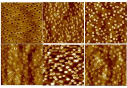
We analyzed the surface morphology of the nano-rings with different growth conditions as shown in Figure 1. We found that there are at least three significant features exhibited in the surface morphology. Above all, crater-like nanoholes were formed even though the capped QDs were cooled down immediately without annealing. However, there is no depression in the center for the uncapped QDs. Based on the significant features exhibited on the surface morphologic changes, we can give a simple conclusion: nano-rings formation is a two-step process. The initial process for depression in the center is originated from an unbalanced outward force caused by wetting droplet instability. However, the temperature and the time of annealing, as well as the alloying effect during capped GaAs strongly influence the migration behavior of out-diffusive In atoms, leading to a variety of surface morphology.
Magneto-Optical Properties of Nano-Rings
A further consequence of the unusual topology is that the center hole enables trapping of a single magnetic flux and offers the exciting possibility to observe electronic wave-function phases in magneto-optical experiments. This leads to a new so-called ''optical'' Aharonov-Bohm (AB) effect, which can occur only in semiconductor nano-rings. Apart from the thorough theoretical analysis in, no studies are known about the direct optical observation of the AB effect, involving interband transitions. To reveal the full strength of a direct optical investigation, e.g. by
means of near infrared ellipsometry, a more detailed theoretical description of the optical response of nano-ring systems is necessary. Such study can make the precision and versatility of this technique applicable to the study of nano-rings. In our study we show that the interband magneto-optical response of a layer of InAs/GaAs nano-rings (reflectance, transmittance) demonstrates AB oscillations. We develop the theory of optical AB effects beyond the single nano-ring picture and show that these AB effects are within the range of a modern ellipsometric setup
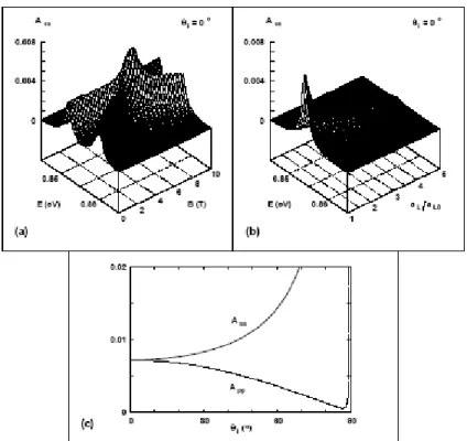
We analyzed the dependency of the calculated polarizability tensor on magnetic field and frequencies near the quantum ring absorption edge for a lattice of InAs/GaAs nano-rings as shown in Figure 1. Interesting behavior of the polarization tensor of a quantum ring in a magnetic field can be observed clearly in Figure 2. The crossing of the transition energies results in oscillations in the real and imaginary part of the polarizability. The polarizability reflects directly the optical AB effect. This effect is directly related to the magnetic field dependence of the energy levels belonging to the ground state Hamiltonian of the quantum rings. It dominates in the magnetic field dependence of the optical response and has to be distinguished from the weaker Faraday/Kerr and Cotton/Mouton effects. Figure 3 shows the absorbance of the layer of rings. The absorbance inherits the oscillatory behavior of the polarization tensor and reflection coefficients. We stress that the magnitude depends strongly on the average concentration of the rings. Hence to demonstrate unambiguously the optical AB effect ellipsometrically, the highest possible lattice density should be used. The most dramatic feature of the absorbance is the large difference in the dependence As (s-polarized light) and Ap (p-polarized light) on the angle of
incidence (Figure 3). It is definitely not a Brewster minimum related feature. The calculated results suggest a large polarization anisotropy for absorbance at large angles of incidence. This can be measured and should display the new optical AB effects for low temperature and moderate magnetic field regimes.
Publications:
1. B. C. Lee, O. Voskoboynikov and C. P. Lee, III-V semiconductor nano-rings, Physica E, accepted, to appear in 2004.
2. O. Voskoboynikov, C.M.J. Wijers, J.L. Liu, and C. P. Lee, Interband Magneto-Optical Transitions in a Layer of Semiconductor Nano-Rings, submitted to Phys. Rev. Lett.
3. O. Voskoboynikov, O. Bauga, C. P. Lee, and O. Tretyak, Magnetic properties of parabolic quantum dots in the presence of the spin-orbit interaction, Journal of Applied Physics, 94, 5891 (2003).
4. B. C. Lee, O. Voskoboynikov and C. P. Lee, III-V semiconductor nano-rings, Abstracts of the
International Symposium on Functional Semiconductor NanoSystems, November 12-14, 2003,
NTT Atsugi R&D Center (Japan).
5. O. Voskoboynikov, C.M.J. Wijers, J.L. Liu, and C. P. Lee, Magneto-optical response by a layer of semiconductor nano-rings, accepted for presentation in The 20th General Conference of the
Condensed Matter Division of the European Physical Society, July 19-23, 2004, Prague (The
Figures:
Figure 1. The surface morphology of quantum rings with different growth conditions
Figure 2. Schematic diagram of magneto-optical phenomena in a layer of nano-rings. (a) Schematic InAs/GaAs ''eye'' shaped nano-ring (after TEM picture). (b) Transition energy as a function of magnetic field for electron angular momentum quantum number me=0 and hole angular momentum quantum number mh=0, and me= mh=-1 optical
Figure 3. Polarizability tensor elements (normalized) for the InAs/GaAs nano-rings, shown in Fig. 1. (a) Real part of αxx=αyy. (b) Imaginary part of idem.
Figure 4. Optical absorbance by a layer of InAs/GaAs nano-rings. (a) ss-type of absorbance at
θi=0. (b) Peak value of ss-type absorbance as shown at (a) for varying lattice parameter
aL and energy ħω (B≈ 6 T ). (c) As (b) for both types of absorbance, but now for
varying θi only ħω≈0.584 eV and B≈ 6 T)