Growth and Field Emission of Reactive Sputtered Pd–PdO
Core–Shell Nanoflakes on Platinum
Chien-Jung Huang,aFu-Ming Pan,a,zTai-Cheng Tzeng,aLi-Chang,aand Jeng-Tzong Sheub
a
Department of Materials Science and Engineering andbInstitute of Nanotechnology, National Chiao-Tung University, Hsinchu, 30010 Taiwan
Palladium oxide共PdO兲 was deposited on platinum by reactive sputter deposition, and the PdO thin film grown on the Pt substrate had a flakelike morphology. The nanosized flake had a core–shell structure with a single Pd grain encapsulated by a crystalline PdO surface layer. The formation of the PdO capped nanoflakes was ascribed to a large interfacial stress due to a lattice mismatch between PdO and Pt. Field emission characteristics of the nanoflakes were studied and a field-enhancement factor of 791 was obtained.
© 2008 The Electrochemical Society. 关DOI: 10.1149/1.3035822兴 All rights reserved.
Manuscript submitted September 30, 2008; revised manuscript received October 24, 2008. Published December 4, 2008.
Palladium oxide共PdO兲 is a p-type semiconductor with a bandgap of 0.8–2.2 eV.1-3It is thermally stable up to⬃800°C, at which the oxide decomposes into the metallic Pd state.2 Because of various particular chemical, optical, and electrical properties, PdO is of great importance in many technological applications, such as catalysis,4,5 photoelectrolysis,6and electron field emission.7Nanomaterials usu-ally exhibit distinct material properties from bulks due to a large surface-to-volume ratio and the quantum-confined electronic struc-ture. PdO nanostructures have recently been prepared and investi-gated for their intriguing properties. For instance, PdO nanofibers have been synthesized by electrospinning using palladium acetate/ polycarbonate solutions,8and nanotips were produced by relaxing large compressive stresses during thermal oxidation of Pd films.9In this study, we used reactive sputter deposition to deposit PdO thin film on the Pt substrate, and found that nanosized flakes with a core–shell structure, in which a Pd grain was encapsulated by a crystalline PdO layer, were produced. Many two-dimensional共2D兲 nanomaterials, such as nanowalls,10nanosheets,11and nanoflakes,12 have been widely studied, such the 2D core–shell nanostructure. The possible growth mechanism of the core–shell nanoflake and field-emission properties of the nanoflakes are discussed in this paper.
Experimental
Deposition of PdO nanoflakes was carried out in a radio-frequency共rf兲 magnetron sputter deposition system. The palladium target was 2 in. in diameter with a purity of 99.99%. Reactive sput-ter deposition was performed with a gas mixture of Ar共20 sccm兲 and O2共20 sccm兲 at the working pressure of 9 ⫻ 10−3Torr and the
rf power of 50 W. The sample preparation was started with the thermal growth of a SiO2layer 100 nm thick on a 6 in. p-type共100兲 silicon wafer. A Ti layer 10 nm thick was then deposited by electron-beam evaporation共E-beam兲 on the oxide as an adhesion layer for the subsequently E-beam deposited Pt thin film with a thickness of 30 nm. The nanoflake film was then deposited on the Pt film at various temperatures. The surface morphology of the PdO nanoflake thin film was examined by scanning electron microscopy 共SEM, JEOL JSM-6500F兲, and the chemical composition was char-acterized by X-ray photoelectron spectroscopy 共XPS兲 and Auger electron spectroscopy 共Thermo VG 350兲. X-ray diffractometry 共XRD, PANalytical X’Pert Pro兲 and transmission electron micros-copy共TEM, JEOL JEM-3000F兲 were used to study the microstruc-ture of the nanoflakes. Field-emission measurements of the nanoflakes were carried out under a vacuum condition of 5.0 ⫻ 10−6Torr with a high-voltage measurement source 共Keithley
237兲, using the planar capacitor measurement configuration. The separation between the nanoflake cathode and the indium tin oxide coated anode plate was 100m.
Results and Discussion
Figures1aandbshow the plane-view SEM images of PdO thin films reactive sputter deposited on the Pt substrate for 15 min at 25 and 200°C, respectively. For both the deposition temperatures, the PdO thin films had a flakelike morphology. The 60°-tilted SEM image of the PdO deposited at 200°C shown in Fig.1cindicates that the PdO thin film was composed of many individual fish scalelike flakes vertically standing on the substrate. While the length of the nanoflakes increased with the deposition temperature, the heights of the nanoflakes deposited at 25 and 200°C were the same. PdO nanoflakes deposited at 200°C had a width of ⬃15 to 20 nm, a length of⬃250 to 280 nm, and a height of ⬃200 nm.
The glancing-angle X-ray diffraction spectra of as-deposited nanoflake thin films are shown in Fig.2. For the nanoflakes grown at 25°C, four reflection peaks, corresponding to the共111兲, 共200兲, 共220兲, and共311兲 planes of the Pd face-centered cubic 共fcc兲 structure, were clearly observed, and a small peak situated at 33.8° was identified as the PdO共101兲 plane. As the growth temperature was raised to 200°C, while the four diffraction peaks for metallic Pd were still
z
E-mail: [email protected]
Figure 1. SEM images of Pd–PdO nanoflakes deposited on the Pt substrate at共a兲 25 and 共b兲 200°C. 共c兲 60°-tilted SEM image for nanoflakes deposited at 200°C.
Journal of The Electrochemical Society, 156共2兲 J28-J31 共2009兲
0013-4651/2008/156共2兲/J28/4/$23.00 © The Electrochemical Society
J28
) unless CC License in place (see abstract). ecsdl.org/site/terms_use
address. Redistribution subject to ECS terms of use (see 140.113.38.11
detected with similar intensity ratios, the peak intensity of the PdO共101兲 plane significantly increased and two more peaks due to the PdO共112兲 and 共103兲 planes became obvious. This result indi-cated that the deposited nanoflakes were composed of crystalline Pd and PdO, and the PdO phase deposited at 200°C had a better crys-tallinity than that at 25°C. Also shown in Fig.2are two Pd共3d兲 XPS spectra of nanoflakes deposited separately at 25 and 200°C共inset兲. For both the two deposition temperatures, the Pd共3d5/2兲 peak
situ-ated at⬃336.9 eV corresponds to the chemical state of PdO. No signal at 335.0 eV was detected, indicating that metallic Pd was absent on the surface of the nanoflakes. Combined with the XRD results, the XPS analysis suggested that the nanoflake was capped by a PdO surface layer with a thickness probably larger than five times the inelastic mean-free path of the Pd 共3d兲 photoelectrons 共⬃5 nm兲, and the PdO layer had a strong 共101兲 texturing. A TEM study further showed that a single-crystalline Pd grain was encapsu-lated by the PdO layer.
The TEM images of a nanoflake deposited at 200°C is shown in Fig.3. The nanoflake was separated from the thin film by ultrasonic agitation in ethanol. The observation of Moiré fringes in the TEM image of Fig. 3a indicated that different crystalline phases were present in the thin nanoflake. The inset shows the selected area electron diffraction共SAED兲 pattern of the nanoflake. Two sets of diffraction spots, marked separately by the solid and dashed lines, can be clearly identified from the SAED pattern, revealing that the nanoflake was composed of two single crystalline phases. Because the two diffraction sets have a symmetrical arrangement with respect to each other, the two corresponding-crystals should be epitaxially aligned with each other in the nanoflake. The diffraction set with orientation labels of共02¯2兲, 共11¯1兲, and 共200兲 corresponded to the Pd fcc structure with the zone axis of关011兴, and the other set with labels of 共11¯2兲, 共101兲, and 共110兲 was due to the PdO tetragonal structure with the zone axis of 关1¯11兴. The high-resolution TEM 共HRTEM兲 image of an edge area of the nanoflake 共highlighted by the circle in Fig.3a兲 is shown in Fig.3b. The fringe spacings of 0.269 and 0.218 nm corresponded to the lattice spacings of PdO共101兲 and 共110兲, respectively. The fast-Fourier transform dif-fraction共FFTD兲 pattern 共inset of Fig.3b兲 of the area marked by the
square in the HRTEM image indicated a single-crystalline phase in the edge area of the nanoflake. The TEM analysis clearly demon-strated that the nanoflake had an epitaxial core–shell structure with a Pd single-crystalline grain surrounded by the PdO surface layer.
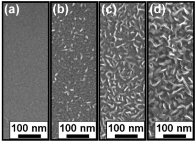
To explore the growth mechanism of the Pd–PdO nanoflakes, we have grown nanoflakes for various deposition times. The SEM
im-ages of Fig. 4 show variation in surface morphology of the nanoflake thin film deposited at 25°C as a function of the deposition time. The thin film deposited for 2 min had a very smooth surface 共Fig.4a兲. Islands began to emerge on the film surface after 3 min
deposition, and a few islands already exhibited a flakelike feature 共Fig. 4b兲. The flakes grew larger both in length and height with
increasing the deposition time, as shown by Fig. 4c and d. The observation implied that the nanoflakes were not directly formed on the substrate via the Volmer–Weber growth mode, but rather evolved due to a certain driving force developing in the early stage of the film deposition. The XPS spectrum of the smooth thin film deposited for 2 min is shown in Fig.5. A close examination of the Pd共3d兲 peaks indicated that, within the probe depth of the XPS measure-ment, PdO was the only chemical state of Pd. Because Pt共4f兲 pho-toelectrons from the substrate were also detected, the presence of metallic Pd in the thin film could be ruled out. Thus, the XPS analy-sis suggested that PdO was the primitive product at the beginning of the reactive sputter deposition, and very likely the precursor for the formation of the crystalline Pd grain in the nanoflake.
Figure 2. 共Color online兲 XRD spectra of Pd–PdO nanoflakes deposited on the Pt substrate at共a兲 25 and 共b兲 200°C. The inset shows the Pd 共3d兲 XPS spectra of nanoflakes deposited at共a兲 25 and 共b兲 200°C.
Figure 3. 共a兲 TEM image of a Pd–PdO nanoflake separated from the nanoflake thin film deposited at 200°C for 15 min. The inset is the SAED pattern of the nanoflake. Two diffraction sets are identified to correspond to the Pd fcc structure共solid line兲 and the PdO tetragonal structure 共dashed line兲. 共b兲 The HRTEM image of the edge area marked by circle in 共a兲. The inset shows the FFTD pattern of the area marked by square in共b兲.
J29
Journal of The Electrochemical Society, 156共2兲 J28-J31 共2009兲 J29
) unless CC License in place (see abstract). ecsdl.org/site/terms_use
address. Redistribution subject to ECS terms of use (see 140.113.38.11
To study the role of the Pt substrate in the growth of the Pd–PdO core–shell nanoflakes, we have also reactive sputter deposited PdO at 200°C on a sputter-deposited Ti and a thermally grown SiO2thin
film for comparison. Nanoflakes with a geometric shape like that shown in Fig.1were also produced on both the thin-film substrates. According to XRD and XPS analyses, PdO was the only chemical composition of the nanoflakes deposited on the Ti and SiO2
sub-strates. In addition, TEM analysis showed that the PdO nanoflake was a single-crystalline grain共not shown兲. Based on simple surface energy consideration, formation of the crystalline PdO nanoflake rather than a spherical structure suggested that the growth of the PdO nanoflake was via an anisotropic process. The anisotropic growth process might be related to the planar coordination arrange-ment of Pd and oxygen atoms in the PdO crystal lattice, in which each Pd atom is coordinated with four oxygen atoms. Because the nanoflake grown on the SiO2and Ti surfaces was composed of only
the crystalline PdO phase, the Pt surface must play a critical role in the formation of Pd–PdO core–shell nanoflakes on the Pt substrate. The observation that the core–shell nanoflake grown on the Pt sub-strate has the same geometric shape as the crystalline PdO nanoflake grown on the SiO2and Ti substrates seemed to suggest that PdO was first deposited on the Pt substrate, followed by formation of the crystalline Pd core sheet with a shape compliant with that of the PdO nanoflake. This suggestion is in agreement with the discussion about Fig.4and5.
PdO has a crystal structure of tetragonal cooperite structure with the lattice constants a = b = 3.0434 Å and c = 5.3363 Å.13The Pt fcc structure has lattice constants a = b = c = 3.924 Å, which are very close to the lattice constants of the Pd fcc structure 共a = b = c = 3.891 Å兲. As the PdO film grew thicker, the interfacial stress between the PdO deposit and the Pt substrate became so large, due to the large lattice mismatch, that decomposition of the PdO phase and lattice reconstruction could be initiated at the interface. Further-more, the negligible difference in the lattice parameters between the Pd and Pt lattices共0.8%兲 could facilitate nucleation of the Pd crystal on the Pt substrate during the initial stage of the phase transforma-tion. The lattice mismatch between the PdO and Pd lattices was very large as well; thereby, a large interfacial stress always existed at the PdO–Pd interface. Therefore, the phase transformation from PdO into Pd must progressively proceed at the interface between the growing Pd crystal and the PdO surface layer, which was continu-ously deposited on the nanoflake during the reactive sputter deposi-tion. The continuous stress building up between the Pd core sheet and the PdO surface layer would limit the thickness of the PdO layer deposited on the nanoflake. According to the XPS and HRTEM analyses, the PdO surface layer was probably⬃4 to 6 nm in thick-ness. Because the thickness of the nanoflake was⬃15 to 20 nm as discussed above, the Pd core sheet in the nanoflake must be just a few nanometers in thickness. From the SAED diffraction pattern shown in Fig.3a, the PdO surface layer was epitaxially aligned with the Pd crystal. It has been previously reported that the PdO共110兲 plane was epitaxially aligned with the Pd共200兲 plane when Pd par-ticles supported on SiO2were oxidized in oxygen.14The same
epi-taxial arrangement was also observed in this study. The lattice spac-ing of the PdO共110兲 and the Pd共200兲 planes are 2.11 and 1.95 Å, respectively. Compared with other lattice planes of the two crystal structures, these two planes have the smallest difference in the lat-tice spacing, and are more likely to be epitaxially arranged with each other. Within this thickness range of the PdO surface layer, the ep-itaxial arrangement of the Pd–PdO core–shell structure seemed to be relatively stable.
PdO is a semiconductor and, therefore, not an ideal field-emission material in respect to its relatively high electrical resistiv-ity. However, the metallic Pd core sheet can increase the conductiv-ity of the Pd–PdO core–shell nanoflake as a whole, and thereby may improve the field-emission efficiency. Moreover, because the nanoflakes vertically standing on the substrate had a sharp top edge and a high aspect ratio in terms of the thickness and height, they are expected to have good field-emission properties. Figure6shows the field-emission current density–applied field共J-E兲 curves of the PdO Figure 4. SEM images of Pd–PdO nanoflakes deposited on the Pt substrate
at 25°C for共a兲 2, 共b兲 3, 共c兲 4, and 共d兲 5 min.
Figure 5. XPS survey spectra for 2 min deposition at a substrate temperature of 25°C.
Figure 6. 共Color online兲 Field-emission J-E curves of Pd–PdO nanoflakes deposited on the Pt substrate at共a兲 25 and 共b兲 200°C. The corresponding FN plots of the J-E curves共a兲 and 共b兲 are shown in the inset.
J30 Journal of The Electrochemical Society, 156共2兲 J28-J31 共2009兲
J30
) unless CC License in place (see abstract). ecsdl.org/site/terms_use
address. Redistribution subject to ECS terms of use (see 140.113.38.11
nanoflakes deposited for 15 min at 25 and 200°C. According to the J-E curve, nanoflakes deposited at 200°C had a much better field-emission performance than that deposited at 25°C. At the applied field of 11 Vm−1, nanoflakes deposited at 200 and 25°C had a
field-emission current density of 30.7A cm−2and 4 nA cm−2,
re-spectively. The linear Fowler–Nordheim 共FN兲 plots shown in the inset of Fig. 6 indicated that the field emission followed the FN field-emission mechanism. The turn-on field of the nanoflakes de-posited at 25 and 200°C was determined to be 10 and 6 Vm−1,
respectively. The turn-on field was herein defined as the field at the intersection of the two straight lines extrapolated separately from the linear rising segment and the background of the FN plot. The better field-emission characteristics of the nanoflake deposited at 200°C may be attributed to that the PdO surface layer on the nanoflake deposited at 200°C had a well-textured and better crystalline struc-ture than that deposited at 25°C. According to the FN theory,15the field enhancement factor共兲, which is strongly dependent on the geometric structure of the field emitter, can be approximated by
 = − B3/2
S 关1兴
where B = 6.83⫻ 103共V eV−3/2m−1兲, is the work function of
the emitter, and S is the slope of the FN plot. The FN plot slope of the nanoflake deposited at 200°C was −108.3. The values of the nanoflake were thus determined to be 791, assuming a work func-tion of 5.4 eV for PdO.16 The  value of Pd–PdO nanoflakes is comparable to that of Co3O4nanowalls17and some previously re-ported one-dimensional nanoemitters, such as carbon nanotubes and Si nanotips.18,19Due to the desirable field-emission characteristics, combined with an easy preparation method and chemical and ther-mal stabilities, the Pd–PdO nanoflakes can be considered as a po-tential emitter for field-emission applications.
Conclusion
In summary, we have deposited PdO on the Pt substrate by re-active sputter deposition. At temperatures 200°C and below, the PdO thin film grown on the Pt substrate had a flakelike morphology. TEM, XRD, and XPS studies revealed that the nanoflake had a core–shell structure with a single Pd grain encapsulated by a crys-talline PdO surface layer. The PdO layer was about 4–6 nm in thick-ness and epitaxially aligned with the Pd lattice. Formation of the Pd–PdO nanoflakes resulted from the large interfacial stress due to
the large lattice mismatch between the PdO surface layer and the Pt substrate. The Pd grain growth in the nanoflake was facilitated by the close similarity in the lattice parameters of the Pt and Pd fcc crystal structures. Because of the sharp top edge and a high aspect ratio, the Pd–PdO nanoflake exhibited a field emission efficiency comparable to many one-dimensional nanoemitters. A value of 791 was obtained for the nanoflake deposited at 200°C.
Acknowledgments
This work was supported by the National Science Council of Taiwan under contract no. NSC96-2221-E009-109-MY3. Technical support from National Nano Device Laboratories is gratefully ac-knowledged.
National Chiao Tung University assisted in meeting the publication costs of this article.
References
1. E. A. Sales, G. Bugli, A. Ensuque, M. J. Mendes, and F. Bozon-Verduraz, Phys.
Chem. Chem. Phys., 1, 491共1999兲.
2. T. Arai, T. Shima, T. Nakano, and J. Tominaga, Thin Solid Films, 515, 4774 共2007兲.
3. J. R. McBride, K. C. Hass, and W. H. Weber, Phys. Rev. B, 44, 5016共1991兲. 4. P. Gélin and M. Primet, Appl. Catal., B, 39, 1共2002兲.
5. L. V. Nosova, M. V. Stenin, Y. N. Nogin, and Y. A. Ryndin, Appl. Surf. Sci., 55, 43 共1992兲.
6. M. P. Dare-Edwards, J. B. Goodenough, A. Hamnett, and A. Katty, Mater. Res.
Bull., 19, 435共1984兲.
7. E. Yamaguchi, K. Sakai, I. Nomura, T. Ono, M. Yamanobe, N. Abe, and T. Hara, J.
Soc. Inf. Disp., 5, 345共1997兲.
8. P. Viswanathamurthia, N. Bhattarai, H. Y. Kim, D. I. Cha, and D. R. Lee, Mater.
Lett., 58, 3368共2004兲.
9. S. Aggarwal, A. P. Monga, S. R. Perusse, R. Ramesh, V. Ballarotto, E. D. Williams, B. R. Chalamala, Y. Wei, and R. H. Reuss, Science, 287, 2235共2000兲. 10. S. W. Kim, S. Fujita, M. S. Yi, and D. H. Yoon, Appl. Phys. Lett., 88, 253114
共2006兲.
11. Y. C. Yhu and Y. Bando, Chem. Phys. Lett., 372, 640共2003兲.
12. N. G. Shang, F. C. K. Au, X. M. Meng, C. S. Lee, I. Bello, and S. T. Lee, Chem.
Phys. Lett., 358, 187共2002兲.
13. D. B. Rogers, R. D. Shannon, and J. L. Gillson, J. Solid State Chem., 3, 314 共1971兲.
14. S. Penner, B. Jenewein, H. Gabasch, B. Klötzer, D. Wang, A. Knop-Gericke, R. Schlögl, and K. Hayek, J. Chem. Phys., 125, 094703共2006兲.
15. R. H. Fowler, L. W. Nordheim, Proc. R. Soc. London, Ser. A, 119, 173共1928兲. 16. J. Rogal, K. Reuter, and M. Scheffler, Phys. Rev. B, 69, 075421共2004兲. 17. T. Yu, Y. Zhu, X. Xu, Z. Shen, P. Chen, C. T. Lim, J. T. Thong, and C. H. Sow, Adv.
Mater. (Weinheim, Ger.), 17, 1595共2005兲.
18. R. C. Smith, D. C. Cox, and S. R. P. Silva, Appl. Phys. Lett., 87, 103112共2005兲. 19. T. M. Chen, F. M. Pan, J. Y. Hung, S. C. Wu, C. F. Chen, and L. Chang, J.
Electrochem. Soc., 154, D215共2007兲.
J31
Journal of The Electrochemical Society, 156共2兲 J28-J31 共2009兲 J31
) unless CC License in place (see abstract). ecsdl.org/site/terms_use
address. Redistribution subject to ECS terms of use (see 140.113.38.11