Received 11th April 2013, Accepted 24th April 2013 DOI: 10.1039/c3ra41744a www.rsc.org/advances
inexpensive techniques at room temperature; properties usually associated with polymer films. In this study, we demonstrate a simple, low-cost and environmentally friendly method for the high-yield production of two dimensional nanosheets of semiconducting transition metal disulfides, integrated with the route towards the solution-processed deposition of MoS2and WS2thin films. The resulting materials with high purity and no contamination or distortion in their structural and electronic properties were confirmed with different microscopic and macroscopic methods. As a proof of concept, we utilize these layered transition metal disulphide films as electron extraction layers in an inverted structure organic solar cell, prepared at relatively low annealing temperatures (¡150 uC). A promising power conversion efficiency with high stability is achieved, which makes these proposed buffer layers quite attractive for next-generation flexible devices requiring high conductivity and transparency, as well as wide range of other potential applications.
1. Introduction
Because of its desirable combination of excellent thermal, electronic, optical and mechanical properties, graphene has become the most widely studied two-dimensional (2D) material; nevertheless, the absence of an energy gap has retarded its application in logic electronics.1,2Accordingly, it has become necessary to synthesize graphene analogues of layered inorganic materials that have a finite band gap, such as the dichalcogenides of molybdenum and tungsten. Transition metal dichalcogenides (TMDs) are extremely promising building blocks for the development of next-generation nanoelectronics. There are more than 40 different types of TMDs having the stoichiometry MX2, depending on the combination of transition metals (M; e.g. W, Mo, Ti, Nb and Ta) and chalcogen (X; S, Se and Te);3–5they form stacked 2D trilayered X–M–X (e.g. S–W–S) sheets that are stabilized through weak interactions. Each sheet is trilayered with an M atom in the middle covalently bonded to six X atoms located at the top and bottom of the sheet (Scheme 1a). Although the bonding within these trilayer sheets is covalent, adjacent
sheets stack through van der Waals interactions.6–8Depending on the combination of metal and chalcogen, the material can be metallic, semimetallic or semiconducting; for example, tungsten sulfide (WS2) and molybdenum sulfide (MoS2) are semiconductors, whereas niobium selenide (NbSe2) is a metal.3,9 Unlike the poor mobilities of organic semiconduc-tors, semiconducting TMD compounds can have high mobi-lities.10In addition, the electronic properties strongly depend on the number of layers; for instance, single-layer MoS2 and WS2are direct gap semiconductors having gap energies (Eg) of 1.9 and 2.1 eV, respectively, whereas bulk MoS2and WS2are indirect gap semiconductors having values of Eg of 1.2–1.3
eV.4,11–13Nanomaterials based on transition metal disulfides
(MoS2, WS2) have several applications as, for example, super-lubricants,14materials for batteries,15tips for scanning probe microscopes,16 thin film transistors (TFTs),17 field effect transistors (FET),18enhancement and depletion-mode transis-tors,19 light emitting diodes (LEDs), gas sensors,20 hydrogen evaluation catalyst,21–24 Schotky-barrier solar cells,25 bulk heterojunction solar cells26 and UV range photodetectors.27 Several methods have been employed to fabricate TMD thin layers, including scotch tape-assisted micromechanical exfo-liation,28,29 solution exfoliation,3,30,31 intercalation-assisted exfoliation,32,33 atomic layer deposition,34 physical vapor deposition,35 sputtering,36 atomic layer with chemical vapor deposition37 and electrochemical synthesis.38 Although most of these methods can be used to produce good-quality TMD layers, there are several drawbacks: the lateral dimensions are typically small; the processes require high vacuum, high
aDepartment of Physics, National Taiwan University, Taipei 106, Taiwan bNanoscience and Technology Program, Taiwan International Graduate Program,
Academia Sinica, Taipei 115, Taiwan
cResearch Center of Applied Science, Academia Sinica, Taipei 115, Taiwan dInstitute of Atomic and Molecular Sciences, Academia Sinica, Taipei 10617, Taiwan e
Institute of Physics, Academia Sinica, Taipei 115, Taiwan
f
Department of Photonics, National Chiao Tung University, HsinChu, 300, Taiwan. E-mail: gchu@gate.sinica.edu.twa
reaction temperatures, or long reaction times; and the semiconducting properties can be variable.7,33,39 Furthermore, most TMD semiconductors exhibit low solubility and only in solvents that are highly toxic and have high boiling points (e.g. octadecylamine),40making it difficult to achieve a large scalable production and limiting the utility of deposition through solution-processing. Herein, we describe a wet grinding method that is a simple but effective approach for producing few-layer nanosheets in high yields. By employing a spin-casting technique we have assembled exfoliated WS2and MoS2 to form high-quality, continuous thin films at low temperatures (150 uC); these films can be used as electron extraction layers in inverted-structure bulk heterojunction organic solar cells (OSCs). Many 2D materials, in particular graphene, have been used for the fabrication of solar cell,41–45 but to the best of our knowledge, this paper is the first to report OSCs featuring WS2 and MoS2 nanosheets as the electron extraction layer that have a promising power conver-sion efficiency (PCE) and high stability. Unlike previously reported approaches, our solution-based method is relatively simple and cheap. It does not require a third-phase dispersant (i.e. surfactant) and can potentially be scaled up to give large quantities (gram) of exfoliated material.
2. Experimental
2.1 Materials and chemicalsMoS2 (powder, 99%; Sigma–Aldrich), WS2 (powder, 99%; Sigma–Aldrich), MoSe2 (99.9%; Alfa Aesar), NbSe2 (99.9%; Alfa Aesar), BN (hexagonal; 99.5% Alfa Aesar), V2O5 (99.6% min.; Alfa Aesar), aluminium (Al, 99.999%; Admat Midas), ITO (,10 V sq21; RiTdisplay), poly(3-hexylthiophene) (P3HT, Rieke Specialty Polymer), PCBM (.99%; Solenne), holey carbon-coated copper grid (Lacey Carbon Type-A 300 mesh copper grids; TED Pella), EG (J.T. Baker), 1,2-dichlorobenzene (DCB; Aldrich), and methanol (Aldrich) were used as received without further purification. Deionized water was purified using a Milli-Q System (Millipore, Billerica, MA, USA); the detergent
(TFD4) water (Franklab SA, Taiwan) was diluted with deionized water.
2.2 Exfoliation process
The wet grinding mechanism used to prepare the 2D nanosheets is presented in Scheme 1b. First, WS2 and MoS2 powders were mixed with pure ethyleneglycol (EG) at a concentration of 1 wt%. The dark black solution was placed with zirconia beds (size = 100 mm and density . 5.95 g cm23) in a grind container. Mechanical commuting through bead-milling in a wet-grinding instrument was performed for 480 min, with the peripheral speed of the rotor fixed at 2000 rpm. Further, imposing the materials for longer time does not effect the thickness of the resultant nanosheets as observed by microscopic instruments. The impact and friction of the beds on the large aggregated TMDs peeled away a single or a few-layers smaller in size, at which the fractional force breaks the large sized chunk into smaller and thinner pieces, whereas the shear force chips the single or few-layers from the surface. The resultant dark green colour dispersion was purified without any contamination from the zirconia beds, since these beds are highly dense they will precipitate very quickly after grinding to the bottom of the container.
2.3 Solar cell devices
Prior to spin-coating a thin WS2or MoS2film, ITO substrates were cleaned through sonication in detergent-containing water and twice with deionized water (15 min each), dried in an oven over night, and then treated with UV/ozone for 15 min. A stable EG solution of WS2 (MoS2) was spun onto the ITO substrate at 2000 (1500) rpm for 60 s and then the sample was thermally annealed at 150uC for 60 min in air on a hot plate. The thickness of the film was controlled by the volume of the solution and the speed of the spin coater during the spin-coating process. Devices featuring a WS2 (MoS2) interfacial layer were prepared in an inverted ITO–WS2 (MoS2)– P3HT:PCBM–V2O5–Al structure (inset to Fig. 5b). The active layer of the device was spin-coated from a solution containing P3HT : PCBM (1 : 1, w/w) in DCB on top of the WS2 (MoS2) film and dried for 30 min in a covered Petri glass dish (solvent evaporation); the films were then annealed at 130 uC for 30 Scheme 1 (a) Atomic structure of a layered TMD (M, transition metal; S, sulfur). Each layer of MS2comprises covalently bonded one transition metal with two sulfur
atoms, S–M–S. Layers are held together by weak interlayer forces. (b) TMD nanosheets produced through wet grinding of the layered bulk material in EG.
Raman spectroscopy (NT-MDT confocal Raman microscopic system; exciting laser wavelength: 473 nm; laser spot-size: 0.5 mm). Thin films of WS2 and MoS2, processed through spin coating onto ITO surfaces, and the TMD powder before and after grinding were characterized using XRD (PANalytical). Absorption and transmittance spectra of the thin films were recorded using a Jasco V-670 UV-vis-NIR spectrophotometer. The physical thicknesses of WS2 and MoS2 thin films were measured by the step profile of AFM; while the active layer thickness was measured using a Veeco Dektak 150 alpha step surface profiler. Solar cell devices were tested inside a glove box under simulated AM 1.5G irradiation conditions (100 mW cm22) using a Xenon (Xe) lamp-based solar simulator (Thermal Oriel 1000W).
3. Results and discussion
Thermodynamically, the free energy of mixing non-electrolytic systems predominates over the solvent and solute mixing process.46 Favourable mixing occurs when the free energy is negative.30,47 Furthermore, the Hildebrand parameter is related to the total cohesive energy density of the solvent (or solute) and, therefore, represents the entire set of solute– solvent interactions. The Hansen solubility parameter theory classifies these interactions into dispersion, polar and hydro-gen bonding interactions. Thus, the dispersion process requires balancing of the solvent–solvent, solvent–solute and solute–solute binding energies.48 The Hildebrand–Scatchard eqn (1) suggests that the enthalpy of mixing is dependent on the balance of the nanosheet and solvent surface energies:
DHMix/VMixy 2/Tflake(di2dsur)w (1) where DHMixis the enthalpy of mixing, VMixis the total volume of mixture, di~
ffiffiffiffiffiffiffiffi Eisur q
is the square root of the surface energy of phase (i), Tflakeis the thickness of a nanosheet (flake), and Q is the nanosheet volume fraction. Eqn (1) implies that the energy per unit area required to overcome the van der Waals forces so that the nanosheets become dispersed is minimized when the surface energies of the nanosheets and solvent are matched.35,47 For a wide range of TMDs, graphene, hexagonal boron nitride and carbon nanotubes, a good dispersing solvent is one having a surface tension between 40 and 50 mJ m22(surface energy close to 70 mJ m22).3,49Although the strong attraction between the solvent
tures.7,33In this present study, therefore, we used an attrition mill (Scheme 1b) to facilitate the exfoliation and isolation of individual nanosheets through the friction and sheer forces of the beads on the layered materials, obtaining clear dispersions of TMDs in EG (surface tension: 47.7 mJ m22at 25uC) that were stable for relatively long periods of time (three months). To determine the chipping state of the materials dispersed after grinding, we first used scanning electron microscopy (SEM) to examine the initial states of the TMD powders. SEM analysis (Fig. 1a and e) revealed very thick (.100 nm) and disordered network arrangements of 2D sheets (.15 mm) for both WS2and MoS2; in comparison, the ground materials were very thin, separate nanosheets. SEM and atomic force microscopy (AFM) images (Fig. 1c and g) of individual nanosheets revealed a typical average thickness of 2.5 nm. Next, we examined the electronic structures of the WS2 and MoS2 nanosheets using Raman spectroscopy (Fig. 2). The Raman spectrum (excitation = 473 nm) of MoS2featured two main bands at 381.2 and 405.76 cm21 with modes related to E12g and A1g, respectively. The energy difference between these two peaks isy24–25 cm21, corresponding to the Raman signature for MoS2 with 4–5 layers.44 For WS2, these signals appeared at 353.5 and 418.4 cm21, respectively, with an energy difference of y64–65 cm21, corresponding to the Raman signature for WS2 with 3–4 layers.8 In each case, these positions match reasonably well with the observed peaks for stacked crystals; shifts of a few wavenumbers can occur upon exfoliation, leading to a slight disagreement between mea-sured and predicted peak positions. These results are consistent with observations reported in the literature.30,50In addition, the stoichiometry of the resultant nanosheets was confirmed by X-ray photoelectron spectroscopy (XPS) and the energy dispersion spectroscopy (EDS) spectrum. XPS revealed strong Wf7/2,Wf5/2and S2p3/2bands at 31.98, 34.38 and 37.3 eV, respectively, for WS2(Fig. 3a); S2s, Mo3d5/2, and Mo3d3/2 bands at 225.55, 228,47 and 231.5 eV, respectively, for MoS2 (Fig. 3b); and S2P3/2and S2P1/2at 162 and 169.5 eV for both WS2 and MoS2(Fig. 3c). The binding energy positions of the Mo3d, Wf and S2P peaks were assigned to the W+4 and S22 oxidation states in WS2and Mo+4and S22oxidation states in
MoS2.32,51From EDS (Fig. 3d) it can be estimated that the atom
ratio of WS21and MoS21of an individual nanosheet is close to 1 : 2, giving the samples a composition of WS2and MoS2.
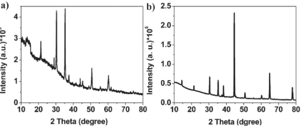
Moreover, X-ray diffraction (XRD) patterns (Fig. 4) revealed the crystal structure of the TMD powders prepared with and without grinding. The nearly identical diffraction angles (2h) of the XRD peaks imply the same degree of crystallinity, with the decreased intensity and broadening of the peaks after grinding being consistent with decreased lateral sizes. All the recorded diffraction peaks of the powders prepared with and without grinding can be mainly indexed to the WS2and MoS2 phase.
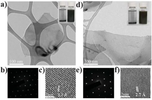
We used transmission electron microscopy (TEM) to further analyse the dispersed materials. Fig. 5a and 5b present TEM images of typical WS2and MoS2nanosheets, respectively; the selected area electron diffraction (SAED) patterns (Fig. 5b and 5e) of the flat areas of the nanosheets and the corresponding high-resolution TEM (HRTEM) images (Fig. 5c and 5f) reveal hexagonal lattice structures having a hexagon width of 2.735 Å and 2.74 Å, assigned to the WS2 and MoS2 (100) planes, respectively, which give a lattice constant of 3.158 Å and
3.164 Å for WS2 and MoS2, respectively, confirming that no distortion occurred upon exfoliation of these 2D materials.32 The few-layers nanosheets were typically a few hundred nanometers in length, in agreement with previous reports.3,30 We attribute the lack of monolayers to the aggregation that occurred during deposition and drying. Furthermore, we performed sedimentation tests of stored dispersions in EG, before and after grinding. The dispersion prepared without grinding precipitated completely within several minutes, but the dispersion prepared with grinding retained its high quality for at least three months after preparation (inset of Fig. 5a and 5d).
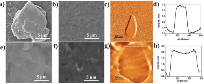
Most methods for the fabrication of thin films of transition metal disulfides require high vacuum, high temperature and complicated chemical syntheses;34,50,52 very little has been reported regarding solution-based deposition. The challenge remains to develop simple methods for the preparation of high-quality 2D nanosheets and solution-processable at low Fig. 1 (a, b, e, f) SEM images, (c, g) AFM images and (d, h) height profiles of the corresponding AFM topographies (average thicknesses: 2–2.5 nm) of typical nanosheets of (c) WS2and (g) MoS2. SEM images of films formed through spray dispersion on Si/SiO2and annealing (70uC, 10 min) of (a, e) non-ground powders of
WS2and MoS2and (b, f) ground (for 480 min) WS2and MoS2dispersions.
Fig. 2 Raman spectra (l excitation = 473 nm) of 2D nanosheets of transition metal disulfides (a) WS2and (b) MoS2. The samples were prepared by dropping the
dispersion (diluted tenfold with methanol) on a Si/SiO2surface and drying under ambient atmosphere at 70uC for 10 min.
temperature thin film materials that should have a broad range of applications (e.g. in solar cells). Fig. 6 displays a few-layer spin-coated transition metal disulfide thin film that we prepared over large areas. The surface roughness (root-mean-square values) of films prepared from WS2and MoS2solutions were 2.7 nm and 3.2 nm, respectively, indicating the high smoothness of the film compared to the bare ITO surface (rms = 4.22 nm). Therefore, these TMD materials can improve the contact between the active material and the ITO surface and
thereby enhance the device performance. We obtained the values of Eg of the as-deposited thin films on ITO-coated glass substrates by extrapolating the straight line portion of the curve to zero absorption coefficients (Fig. 6c and f), as determined from the equation53
lg~
hc Eg~
1240
Eg (2)
Fig. 3 XPS data of the binding energies of (a) W, (b) Mo and (c) S atoms in WS2and MoS2multilayers prepared by placing drops of dispersions onto Si/SiO2wafers
and drying under an ambient atmosphere at 70uC for 10 min. (d) A representative EDS spectrum collected from an individual nanosheet indicating that the material is WS2and MoS2, respectively. Cu peaks came from the holey carbon-coated copper grid.
Fig. 4 XRD patterns of the TMD powders of (a) WS2and (b) MoS2prepared with and without grinding for 420 min. Periodicity in the c-axis is evident for the bulk
materials, with a strong (002) peak observed at a value of 2h of 14u. Diffraction peaks are indexed from the WS2phases (reference code. 008-0237) and MoS2
(reference code. 024-0513).
The values of Egfor the thin films of WS2and MoS2are 1.75 and 1.72 eV, respectively, which match well with the experimentally determined indirect band gaps for their few-layer films.12,54It has been shown that when periodicity in the c-axis is present in bulk materials, a strong (002) peak is usually observed at a value of 2h around 14u (Fig. 4),3,7,32 in contrast, this signal of the (002) plane was barely detectable in
our thin films (see Fig. 7), which suggests the successful fabrication of ultrathin films (few-layers).
Next, as proof of principle we used the uniform continuous films (without pinholes or cracks), which we formed from the grinding of WS2and MoS2solutions, spin-coating and thermal annealing at relatively low temperatures (¡150uC), as electron extraction layers in the fabrication of highly stable
inverted-Fig. 6 SEM and tapping-mode AFM images of transition metal disulfide thin films formed through the spin-coating of dispersions onto ITO surfaces and annealing (150uC, 60 min): (a, b) WS2spin-coated at 2000 rpm; (d, e) MoS2spin-coated at 1500 rpm. UV absorption spectrum of (c) a WS2thin film and (f) a MoS2thin film.
Fig. 5 (a, d) TEM images, (b, e) SAED patterns and (c, f) HRTEM images of (a–c) a typical single-layer WS2nanosheet and (d–f) a typical single-layer MoS2nanosheet.
Inset of (a) and (d) are the sedimentation tests of dispersions before and after grinding for 480 min in EG: (a) WS2(starting concentration: 1 wt%), (d) MoS2(starting
concentration: 1 wt%).
structure OSCs. The current density–voltage (J–V) character-istics of the devices are shown in Fig. 8a; Table 1 summarizes their extracted device parameters. A comparable PCE with the control device prepared with other metal oxides electron extraction layer as reported in our previous work55,56have been achieved. The variations in device performance were not
significant in terms of open-circuit voltages (VOC), possibly because of same potential barrier alignment (same band gap) with the same thickness (around 10 nm) with the active layer materials. In contrast, the device incorporating the MoS2 buffer layer (PCE = 3.23%) had a higher short-current density (Jsc= 11.19 mA cm22) than that of the device featuring a WS2 buffer layer (PCE = 2.93%; Jsc = 9.31 mA cm22), presumably because MoS2 materials have higher conductivities (approxi-mately tenfold),57 lower series resistances (Rs = 0.96 V) measured from the dark current (inset to Fig. 8a) and lower absorption coefficients relative to those of WS2(Fig. 6c and f). The mechanism behind our device may be related to the deposition of high electron affinity materials, namely the electron extraction layer at the anode that increased the photocurrent extraction by reducing the extraction barrier heights and reducing the recombination at the electrodes. Decreasing the energy barrier that the carriers must overcome Fig. 7 XRD patterns of TMD thin films deposited from ground dispersions onto ITO glass: (a) a WS2solution spin-coated at 2000 rpm and then thermally annealed at
150uC for 60 min; (b) a MoS2solution spin-coated at 1500 rpm and then thermally annealed at 150uC for 60 min. For each thin film, it was more difficult to
distinguish the signal for the (002) plane, near a value of 2h of 14u, relative to that for its bulk powder, which further confirms the fabrication of ultrathin films (few-layers).
Fig. 8 (a) Illuminated J–V curves for inverted device structures featuring WS2and MoS2as the buffer layer. Inset: Dark J–V curves. (b) Stability of solar cell devices
featuring WS2and MoS2as electron extraction layers, measured in terms of the PCE over time. Inset: inverted device structure.
Table 1 Device performance parameters of inverted P3HT:PCBM solar cells fabricated with WS2/MoS2thin films as the electron extraction layer
Buffer layer VOC(V) JSC(mA cm22) FF (%) PCE (%) Rs(V)a
WS2 0.58 9.31 55.28 2.98 2.85
MoS2 0.58 11.19 51.6 3.35 0.96
aDevice series resistance (Rs) of the OSC obtained from the inverse slope of the dark J–V curve.
or tunnel through at the electrode emissive layer interface will lead to a high injection efficiency.58 We therefore further investigated the effect of the inserted WS2and MoS2interlayer thicknesses on the device performance. Small variations in thickness of the films correlated with clear variations in the series resistance of the device, which in turn affects its performance. Meanwhile, devices with a very thick electron extraction layer (y50 nm) give a very poor PCE, which may be correlated with an increase in the resistance and high absorbance of the film, and a control device without the electron extraction layer exhibited a tremendous decreases in VOC, FF and performance, revealing the important role that the these interlayers played in the device performance.
Fig. 8b displays the results of the stability measurements of the as-prepared inverted-structure OSCs prepared with WS2 and MoS2as the electron extraction layers. We observed a very minor decrease in the device efficiency over time (40 days). The average decrease in PCE for the device featuring the WS2 buffer layer was approximately 16%, while the major loss arose from the fill factor, which is related to the change in the active layer and not to the buffer layer. The same could be said for the device incorporating the MoS2buffer layer. The improved stability of the devices featuring transition metal disulfides as cathode buffer layers, relative to those of previously reported highly stable devices incorporating metal oxide buffer layers,59 can be explained in two ways: (i) these transition metal disulfides prevent degradation by providing a larger extraction interface and good electron conduction to the ITO electrode for a longer period of time; (ii) the transition metal disulfides are very stable in ambient environments (in particular, they are barely affected by moisture or oxidation, indeed, both materials are used widely as superlubricants14,60) and thus, a significant decrease in the degradation of the blend polymer is likely.
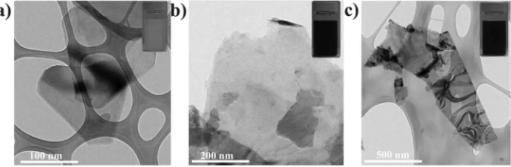
Most importantly, our production method can be applied also to other types of TMD layered materials, including molybdenum(IV) selenide (WSe2, semiconductor) and niobium(IV) selenide (NbSe2, conductor), as well as boron nitride (BN, insulator). Fig. 9 shows typical TEM images of few-layer nanosheets of these materials, which are several hundred nanometers in size. We propose that this technique is a general one that can be applied to other TMDs and BN.
4. Conclusions
In summary, we have developed a novel, simple, efficient and low-cost method for the high-yield production of 2D nanosheets of semiconducting transition metal disulfides, as well as a route towards the solution-processed deposition (through spin-coating) of MoS2 and WS2 thin films from the dispersion. This fabrication approach requires no vacuum processing and was carried out at a relatively low annealing temperature (150uC). We measured the physical and electro-nic characteristics of these TMD layered materials using various spectroscopic (Raman, XRD, XPS) and microscopic (TEM, SEM, AFM) methods. Solar cell devices incorporating WS2 or MoS2 buffer layers in ambient condition exhibited promising PCEs and a high stability. Thus, this new method for preparing TMDs is a very promising one that might enhance the stability and decrease the cost of photovoltaic technologies and other electronic applications.
Acknowledgements
We thank Dr Chun-Wei Pao for helpful discussions and the National Science Council (NSC) Taiwan (NSC 101-2221-E-001-010 and NSC 101-3113-P-009-005) and the Thematic Project of Academia Sinica Taiwan (AS-100-TP-A05) for financial support.
References
1 A. K. Geim and K. S. Novoselov, Nat. Mater., 2007, 6, 183–191.
2 A. K. Geim, Science, 2009, 324, 1530–1534.
3 J. N. Coleman, M. Lotya, A. O’Neill, S. D. Bergin, P. J. King, U. Khan, K. Young, A. Gaucher, S. De, R. J. Smith, I. V. Shvets, S. K. Arora, G. Stanton, H. Y. Kim, K. Lee, G. T. Kim, G. S. Duesberg, T. Hallam, J. J. Boland, J. J. Wang, J. F. Donegan, J. C. Grunlan, G. Moriarty, A. Shmeliov, R. J. Nicholls, J. M. Perkins, E. M. Grieveson, K. Theuwissen, D. W. McComb, P. D. Nellist and V. Nicolosi, Science, 2011, 331, 568–571.
4 W. S. Yun, S. Han, S. C. Hong, I. G. Kim and J. Lee, Phys. Rev. B: Condens. Matter Mater. Phys., 2012, 85.
Fig. 9 TEM images of typical nanosheets of (a) BN ground in IPA at a concentration of 0.75 wt% for 360 min, (b) NbSe2ground in EG at a concentration of 0.5 wt%
for 240 min and (c) WSe2ground in EG at a concentration of 0.5 wt% for 420 min. Insets: images of the ground dispersions (BN in IPA; NbSe2and WSe2in EG).
11 Y. Zhang, J. Ye, Y. Matsuhashi and Y. Iwasa, Nano Lett., 2012, 12, 1136–1140.
12 A. Kuc, N. Zibouche and T. Heine, Phys. Rev. B: Condens. Matter Mater. Phys., 2011, 83.
13 Y. Cheng, Z. Zhu and U. Schwingenschlogl, RSC Adv., 2012, 2, 7798–7802.
14 L. Rapoport, A. Moshkovich, V. Perfilyev, A. Laikhtman, I. Lapsker, L. Yadgarov, R. Rosentsveig and R. Tenne, Tribol. Lett., 2011, 45, 257–264.
15 H. Liu, D. Su, R. Zhou, B. Sun, G. Wang and S. Z. Qiao, Adv. Energy Mater., 2012, 2, 970–975.
16 A. Rothschild, S. R. Cohen and R. Tenne, Appl. Phys. Lett., 1999, 75, 4025.
17 H. Li, Z. Yin, Q. He, X. Huang, G. Lu, D. W. Fam, A. I. Tok, Q. Zhang and H. Zhang, Small, 2012, 8, 63–67.
18 D. J. Late, B. Liu, H. S. S. R. Matte, V. P. Dravid and C. N. R. Rao, ACS Nano, 2012, 6, 5635–5641.
19 H. Wang, L. Yu, Y.-H. Lee, Y. Shi, A. Hsu, M. L. Chin, L.-J. Li, M. Dubey, L.-J. Kong and T. Palacios, Nano Lett., 2012, 12, 4674–4680.
20 Q. He, Z. Zeng, Z. Yin, H. Li, S. Wu, X. Huang and H. Zhang, Small, 2012, 8, 2994–2999.
21 D. Merki and X. Hu, Energy Environ. Sci., 2011, 4, 3878–3888.
22 A. B. Laursen, S. Kegnaes, S. Dahl and I. Chorkendorff, Energy Environ. Sci., 2012, 5, 5577–5591.
23 P. D. Tran, M. Nguyen, S. S. Pramana, A. Bhattacharjee, S. Y. Chiam, J. Fize, M. J. Field, V. Artero, L. H. Wong, J. Loo and J. Barber, Energy Environ. Sci., 2012, 5, 8912–8916. 24 Z. Li, W. Luo, M. Zhang, J. Feng and Z. Zou, Energy Environ.
Sci., 2013, 6, 347–370.
25 M. Shanmugam, C. A. Durcan and B. Yu, Nanoscale, 2012, 4, 7399–7405.
26 M. Shanmugam, T. Bansal, C. A. Durcan and B. Yu, Appl. Phys. Lett., 2012, 100, 153901.
27 S. Alkis, T. O¨zta, L. E. Aygu¨n, F. Bozkurt, A. K. Okyay and B. Ortaç, Opt. Express, 2012, 20, 21815–21820.
28 A. Splendiani, L. Sun, Y. Zhang, T. Li, J. Kim, C. Y. Chim, G. Galli and F. Wang, Nano Lett., 2010, 10, 1271–1275. 29 B. Radisavljevic, M. B. Whitwick and A. Kis, ACS Nano,
2011, 5, 9934–9938.
30 G. Cunningham, M. Lotya, C. S. Cucinotta, S. Sanvito, S. D. Bergin, R. Menzel, M. S. P. Shaffer and J. N. Coleman, ACS Nano, 2012, 6, 3468–3480.
31 K. Zhou, S. Jiang, C. Bao, L. Song, B. Wang, G. Tang, Y. Hu and Z. Gui, RSC Adv., 2012, 2, 11695–11703.
32 Z. Zeng, Z. Yin, X. Huang, H. Li, Q. He, G. Lu, F. Boey and H. Zhang, Angew. Chem., Int. Ed., 2011, 50, 11093–11097.
38 Q. Li, J. T. Newberg, E. C. Walter, J. C. Hemminger and R. M. Penner, Nano Lett., 2004, 4, 277–281.
39 X. Rocquefelte, F. Boucher, P. Gressier, G. Ouvrard, P. Blaha and K. Schwarz, Phys. Rev. B: Condens. Matter, 2000, 62, 2397–2400.
40 G. Gao, W. Gao, E. Cannuccia, J. Taha-Tijerina, L. Balicas, A. Mathkar, T. N. Narayanan, Z. Liu, B. K. Gupta, J. Peng, Y. Yin, A. Rubio and P. M. Ajayan, Nano Lett., 2012, 12, 3518–3525.
41 Z. Yin, S. Wu, X. Zhou, X. Huang, Q. Zhang, F. Boey and H. Zhang, Small, 2010, 6, 307–312.
42 Y. Wang, S. W. Tong, X. F. Xu, B. O¨zyilmaz and K. P. Loh, Adv. Mater., 2011, 23, 1514–1518.
43 Y. Zhou, C. Fuentes-Hernandez, J. Shim, J. Meyer, A. J. Giordano, H. Li, P. Winget, T. Papadopoulos, H. Cheun, J. Kim, M. Fenoll, A. Dindar, W. Haske, E. Najafabadi, T. M. Khan, H. Sojoudi, S. Barlow, S. Graham, J.-L. Bre´das, S. R. Marder, A. Kahn and B. Kippelen, Science, 2012, 336, 327–332.
44 J.-H. Huang, J.-H. Fang, C.-C. Liu and C.-W. Chu, ACS Nano, 2011, 5, 6262–6271.
45 Y. Bi, Y. Yuan, C. L. Exstrom, S. A. Darveau and J. Huang, Nano Lett., 2011, 11, 4953–4957.
46 L. I. Stiel, AIChE J., 1971, 17, iv–iv.
47 Y. Hernandez, V. Nicolosi, M. Lotya, F. M. Blighe, Z. Sun, S. De, I. T. McGovern, B. Holland, M. Byrne, Y. K. Gun’Ko, J. J. Boland, P. Niraj, G. Duesberg, S. Krishnamurthy, R. Goodhue, J. Hutchison, V. Scardaci, A. C. Ferrari and J. N. Coleman, Nat. Nanotechnol., 2008, 3, 563–568.
48 S. D. Bergin, Z. Sun, D. Rickard, P. V. Streich, J. P. Hamilton and J. N. Coleman, ACS Nano, 2009, 3, 2340–2350. 49 S. Stankovich, D. A. Dikin, R. D. Piner, K. A. Kohlhaas,
A. Kleinhammes, Y. Jia, Y. Wu, S. T. Nguyen and R. S. Ruoff, Carbon, 2007, 45, 1558–1565.
50 K.-K. Liu, W. Zhang, Y.-H. Lee, Y.-C. Lin, M.-T. Chang, C.-Y. Su, C.-S. Chang, H. Li, C.-Y. Shi, H. Zhang, C.-S. Lai and L.-J. Li, Nano Lett., 2012, 12, 1538–1544.
51 M. A. Baker, R. Gilmore, C. Lenardi and W. Gissler, Appl. Surf. Sci., 1999, 150, 255–262.
52 J. Pu, Y. Yomogida, K. K. Liu, L. J. Li, Y. Iwasa and T. Takenobu, Nano Lett., 2012, 12, 4013–4017.
53 W. G. J. H. M. van Sark, A. Meijerink, R. E. I. Schropp, J. A. M. van Roosmalen and E. H. Lysen, Sol. Energy Mater. Sol. Cells, 2005, 87, 395–409.
54 K. K. Kam and B. A. Parkinson, J. Phys. Chem., 1982, 86, 463–467.
55 M. A. Ibrahem, H.-Y. Wei, M.-H. Tsai, K.-C. Ho, J.-J. Shyue and C. W. Chu, Sol. Energy Mater. Sol. Cells, 2013, 108, 156–163.
56 J.-H. Huang, T.-Y. Huang, H.-Y. Wei, K.-C. Ho and C.-W. Chu, RSC Adv., 2012, 2, 7487–7491.
57 W. Ki, X. Huang, J. Li, D. L. Young and Y. Zhang, J. Mater. Res., 2011, 22, 1390–1395.
58 R. H. Friend, R. W. Gymer, A. B. Holmes, J. H. Burroughes, R. N. Marks, C. Taliani, D. D. C. Bradley, D. A. D. Santos, J. L. Bredas, M. Logdlund and W. R. Salaneck, Nature, 1999, 397, 121–128.
59 S. Sanchez, S. Berson, S. Guillerez, C. Le´vy-Cle´ment and V. Ivanova, Adv. Energy Mater., 2012, 2, 541–545.
60 M. Praveena, C. D. Bain, V. Jayaram and S. K. Biswas, RSC Adv., 2013, 3, 5401–5411.