Oxidation of Ta diffusion barrier layer for Cu metallization in
thermal annealing
Kai-Min Yin
a, Li Chang
b,U, Fu-Rong Chen
a, Ji-Jung Kai
a, Cheng-Cheng Chiang
a,
Graham Chuang
a, Peijun Ding
c, Barry Chin
c, Hong Zhang
c, Fusen Chen
ca
Department of Engineering and System Science, National Tsing Hua Uni¨ersity, Hsinchu, Taiwan 300, ROC
b
Department of Materials Science and Engineering, National Chiao Tung Uni¨ersity, Hsinchu, Taiwan 300, ROC
c
Metal Deposition Products Group, Applied Materials, Santa Clara, CA 95054, USA
Received 28 January 2000; received in revised form 15 June 2000; accepted 12 December 2000
Abstract
This work examines the thermal stability of Ta barrier layer for Cu metallization with the effect of oxygen. The CurTarSiO rSi2
films were annealed at temperatures ranging from 400 to 600⬚C under various vacuum conditions. Transmission electron microscopy has been performed to characterize the microstructure of the films after annealing. The results show that an amorphous interlayer of oxide between Cu and Ta can be formed at 400⬚C in a vacuum of 10y2 mbar. X-Ray energy dispersive spectroscopy and electron energy loss spectroscopy confirm that this interlayer is tantalum oxide. This interlayer transformed into a crystalline phase of Ta᎐Cu oxide at 600⬚C. In addition, formation of tantalum oxide interlayer is more thermodynamically favorable than that of copper oxide layer at the CurTa interface. Growth of the amorphous interlayer is atmosphere-dependent, as evidenced by the thickness of tantalum oxide being decreased with better vacuum or argon gas. This observation suggests that the oxidation source may arise from the annealing atmosphere rather than from interior SiO . Furthermore, it has been observed2
that oxygen diffuses along grain boundaries in copper films to cause tantalum oxidation.䊚 2001 Elsevier Science B.V. All rights reserved.
Keywords: Cu metallization; Diffusion barrier; Oxidation; Transmission electron microscopy
1. Introduction
Ž .
With a lower bulk electrical resistivity 1.68⍀ cm and better resistance to electromigration than
w x
aluminum and aluminum alloys 1,2 , Cu is highly at-tractive for interconnections in sub-0.25m ultra-large
Ž .
scale integration ULSI device applications. Despite the increasing application of Cu metallization in commercial ULSI device fabrication, several issues re-lated to processing with Cu for future devices of smaller
UCorresponding author. Tel.:q886-3-573-1615; fax: q886-3-572-4727.
Ž .
E-mail address: [email protected] L. Chang .
sizes have not been clarified. According to previous investigations, Cu is a fast diffusion species in silicon
w x
oxide and silicon 3,4 and causes deep-level trapping which seriously degrades the electronic properties of
w x
silicon devices 5 . Other drawbacks include susceptibil-ity to oxidation, corrosion and high chemical reactivsusceptibil-ity w x6 . Among these drawbacks, a diffusion barrier against copper plays a major role in Cu metallization. Recent investigations have conferred that Ta is a promising material as a diffusion barrier layer for Cu
metalliza-w x
tion because Ta and Cu are mutually insoluble 7᎐16 . In addition, Ta has a relatively low resistivity of ;100 ⍀ cm. Although the thermal stability of CurTarSiO rSi structure has received considerable2
w x
attention 17,18 , interfacial structures between the
lay-0040-6090r01r$ - see front matter 䊚 2001 Elsevier Science B.V. All rights reserved. Ž .
ers in nanometer scale which may affect the barrier properties have seldom been studied in detail.
In this investigation, we study the microstructures of barriers and Cu after thermal annealing in various environments to elucidate the oxygen effect on barri-ers. The high affinity of Ta for oxygen enhances the oxide formation, resulting in structural changes of Ta. The microstructural and compositional evolutions at the CurTarSiO interfaces are also investigated by2 cross-sectional transmission electron microscopy ŽTEM . In addition, Cu. rTarSiO rSi films were an-2 nealed at temperatures ranging from 400 to 900⬚C in different atmosphere andror pressures.
2. Experimental details
CurTarSiO rSi structure in blanket films was used2 in this study. The Cu and Ta films were deposited on 8-inch silicon wafers in an Applied Materials ElectraTM
Ž .
system which utilized ion metal plasma IMP process-w x
ing technology 19 . The base pressure of the IMP chambers was typically ;10y8 mbar. The stacking sequences and thickness of the deposited films were Cu Ž150 nm.rTa 25᎐30 nm rSiO 1000 nm on Si wafers.Ž . 2Ž . To investigate the relation between thermal stability and temperature, samples were annealed at various temperatures from 400 to 900⬚C in a vacuum furnace at a pressure of 10y2 torr. A couple of samples were
Ž .
treated at 500 and 600⬚C in pure argon 4 N atmo-sphere at a pressure of 3 mtorr. Before feeding with Ar gas, the furnace was purged several times with Ar and evacuated to 10y2 torr range. All samples were sliced into 1=1 cm2, before annealing. Annealing time for all treatments was 30 min.
Wedge method with grinding and polishing has been w x used to prepare cross-sectional TEM specimens 20 . The final step is ion milling to perforation. A JEOL 2010F field-emission TEM, equipped with an X-ray
Ž .
energy dispersive spectrometer EDS and a Gatan
Ž .
imaging filter GIF was used to investigate the mi-crostructures with chemical compositions. Electron
en-Ž .
ergy loss spectroscopy EELS was performed with the GIF system. All EDS and EELS spectra were obtained by using a 0.5-nm diameter electron beam. Mo or Ni grids were used to mount TEM specimens to prevent the EDX signal from Cu films in the samples from being interfered with that from the Cu grid.
3. Results
3.1. Room-temperature aging effect on TEM specimens
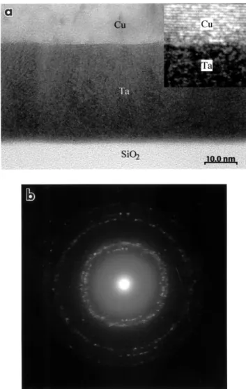
Fig. 1a displays a typical cross-sectional
high-resolu-Ž . Ž
tion TEM HRTEM image enlargement section shown .
in the inset from an as-deposited CurTarSiO rSi2 sample, taken immediately after TEM specimen
prepa-ration. No reaction or formation of any interlayer between stacking layers can be observed, implying that the as-deposited film is clean and has no contamination or oxidation from the environment. The TEM image
Ž .
with selective area diffraction pattern SADP in Fig. Ž
1b shows that Ta is a beta-phase bct, body-center-te-.
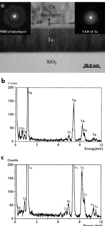
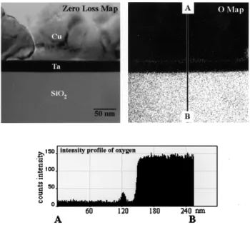
tragonal structure in the form of nanocrystallinity. This TEM sample was re-examined after being stored in air at room temperature for 1 week. Fig. 2a reveals an interlayer of thickness from 2 to 4 nm between Cu and Ta. Nanobeam diffraction pattern from this region shows a diffused ring, indicating that it is amorphous. The thickness of Ta reduced from 30 nm in the as-de-posited condition to 28 nm, as a result of formation of a 2-nm thick interlayer. Fig. 2b,c are the EDS spectra from the interlayer and the Ta film, respectively. Ap-parently, the interlayer contains a significant amount of oxygen, while the oxygen content in the Ta film is negligible. EELS maps in Fig. 3, obtained from another area, display the zero loss map and distribution of Cu, Ta and O. The elemental maps were taken at Cu L
Ž .
Fig. 1. a Cross-sectional TEM image from an as-deposited Ž .
edge of 931 eV, Ta O edge of 36 eV and O K edge of 532 eV with a width of energy window from 5᎐40 eV. An intensity profile across the interface clearly reveals strong oxygen signals at the interlayer that corresponds to the white contrast in Fig. 3c. Notably, the Cu and Ta maps confirm that interdiffusion of Cu and Ta has not occurred yet at room temperature. The results clearly demonstrate the interlayer of amorphous tantalum
ox-Ž .
Fig. 2. a Cross-sectional TEM image of the same TEM sample as used in Fig. 1 which was re-examined after it was kept in air at room temperature for 1 week. A nanobeam diffraction pattern from the
Ž . Ž .
interlayer in insets. b and c EDS spectra obtained from the interlayer and Ta film, respectively.
Fig. 3. EELS maps from different regions in the same CurTarSiO rSi sample as used in Fig. 2.2
ide between Cu and Ta layers can form at room tem-perature for 1 week. The oxidation occurred at the interface between Cu and Ta layers rather than between Ta and SiO . To avoid the aging effect of oxygen, the2 following TEM observations were made immediately after TEM specimen preparation.
3.2. Vacuum annealing
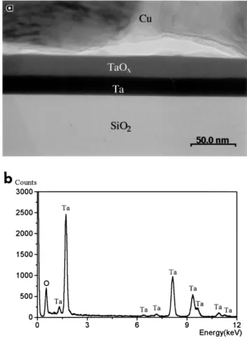
After thermal annealing of the as-deposited samples at 400⬚C for 30 min in a vacuum of 10y2 torr, the microstructure in Fig. 4a reveals a thick amorphous layer of approximately 20 nm between the Cu and Ta films. The high-temperature treatment enhances the interlayer growth. EDS in Fig. 4b indicates that the amorphous layer is also composed of Ta and O with little Cu. The Ta layer remains to be beta phase. After heat treatment at 500⬚C for 30 min, all metallic Ta transformed into amorphous tantalum oxide with the thickness of tantalum oxide increased to approximately 70 nm, as shown in Fig. 5.
Further annealing at 600⬚C resulted in an 83-nm thick interlayer between Cu and SiO , as shown in Fig.2 6a. Diffraction pattern and lattice image in the insets of Fig. 6a indicate that it is of crystalline structure.
˚
Interplanar spacings of 3.09 and 11.0 A have been identified from this phase. Diffraction patterns from several different zone axes reveal that it has no cubic symmetry. EDS in Fig. 6b indicates that it consists of Ta, Cu and O. Quantitative analysis shows that the atomic ratio of Ta to Cu is approximately 3. Therefore,
Ž .
Fig. 4. a Cross-sectional TEM image after thermal annealing at
y2 Ž .
400⬚C for 30 min in a vacuum of 10 mbar. b EDS spectrum obtained from Ta oxide layer.
the interlayer is a tantalum᎐copper oxide. No known structure of tantalum oxides and tantalum᎐copper ox-ides could be identified with the diffraction patterns
w x after an extensive search of JCPDS files 21 . This Ta᎐Cu oxide can persist up to 900⬚C.
3.3. Annealing in argon atmosphere
Samples were treated in Ar atmosphere at a pressure of 3=10᎐ 3torr to understand whether oxidation of Ta could be avoided. The TEM image in Fig. 7 zero loss map, obtained from a sample annealed at 500⬚C, shows that an oxide layer of 5᎐7-nm thick exists between copper and Ta. For samples treated in Ar atmosphere at 600⬚C, the TEM image in Fig. 8 displays that Ta oxide is in contact with underneath SiO , as well as2 along a Cu grain boundary that are perpendicular to the surface and interfaces. A thin oxide layer parallel to the interface is also found between Cu and Ta. Most of the metallic Ta layer remains between Cu and SiO .2 Also, it is noticed that the interface between Ta and SiO is still very sharp and Ta oxide has no reaction2 with SiO . The results strongly suggest that oxygen2 from outside source diffuses along grain boundaries of
Fig. 5. Cross-sectional TEM image after thermal annealing at 500⬚C for 30 min in a vacuum of 10y2 mbar.
Cu to CurTa interface and Ta is then gradually
oxi-Ž .
dized. The SADPs with EDS not shown indicate that the interlayer is an amorphous Ta oxide and Ta re-mains to be bct phase.
Ž .
Fig. 6. a Cross-sectional TEM image after thermal annealing at 600⬚C for 30 min in a vacuum of 10y2 mbar. SAD patterns and lattice images from the tantalum᎐copper oxide layer are shown in Ž . the insets on the right-hand side and left-hand side, respectively. b EDS spectrum obtained from the tantalum᎐copper oxide layer.
Fig. 7. EELS maps after thermal annealing at 500⬚C for 30 min in argon atmosphere.
3.4. Annealing in air atmosphere
Annealing of the as-deposited samples in ambient air resulted in oxidation of both Ta and Cu. Fig. 9 displays that the Cu film has been oxidized into Cu O at 4002 ⬚C. Notably, there are two layers between Cu and SiO :2 the dark layer in 21-nm thick is bct Ta; and above which is an amorphous Ta oxide in gray contrast with 17-nm thickness.
4. Discussion
The results show that Ta would be oxidized both in vacuum and air annealing. The vacuum annealing re-sults in oxidation of Ta barrier. From room tempera-ture to 500⬚C, an amorphous Ta oxide formed after annealing. The oxide thickness increased with
anneal-Fig. 8. Cross-sectional TEM image after thermal annealing at 600⬚C for 30 min in argon atmosphere.
Fig. 9. Cross-sectional TEM image after thermal annealing at 400⬚C for 30 min in air atmosphere.
ing temperature, to 83 nm after annealing at 500⬚C. Annealing above 600⬚C, the Ta barrier was completely replaced by a crystalline Ta᎐Cu oxide. With addition of Ar gas in low vacuum annealing, the oxide thickness can be significantly reduced to approximately 5᎐7 nm between the Cu and Ta layers. Thus, Ar gas can effectively protect the Ta from oxidation. Also, air annealing can oxidize the Ta layer at 400⬚C. The thick-ness of the oxide layer formed in air and low vacuum is comparable, 20 and 17 nm, respectively. This can be explained as follows. During air annealing, the amount of oxygen supplied is sufficient to oxidize the copper while Ta is partially oxidized. Oxidation rate of copper is significantly higher in air than in vacuum, so that the copper oxide layer formed is thick enough to slow down oxygen diffusion to Ta. Consequently, the tantalum oxidation in air annealing might be retarded to a simi-lar level as in low vacuum annealing. The fact that Ta has a higher oxygen affinity than Cu accounts for why Ta oxidation happens at low temperatures in vacuum annealing conditions. In vacuum annealing, oxygen in residual gas is not enough to oxidize the Cu film but sufficient to oxidize Ta. Also, oxygen may have a fast diffusion rate along Cu grain boundaries, compared with low oxidation rate of Cu in vacuum. Though vacuum ambient can reduce the extent of oxidation of Cu, it can not inhibit oxidation of Ta. Even with Ar protection, Ta can not be completely immune from oxidation at 500⬚C. The fact that Ta is highly suscepti-ble to the residual oxygen content in vacuum is due to its strong oxygen affinity.
Tantalum oxide forms at the interface between Cu and Ta rather than between Ta and SiO simply be-2 w x cause Si has a stronger oxygen affinity than Ta 22 . According to thermodynamic calculations, all the reac-tions of Ta with SiO2 in which the products can be TaSi , Ta Si, Ta Si or Ta O have positive free ener-2 2 5 3 2 5 gies. Hence, it can explain why no reaction occurs
between Ta and SiO even after annealing at tempera-2 tures up to 600⬚C.
Partial oxidation of Ta films starting from the posi-tion where Cu grain boundaries terminated at the Ta films as shown in Fig. 8 obtained from a sample an-nealed at 600⬚C for 30 min in Ar, provides strong evidence that Cu grain boundaries perpendicular to the surface and or interface are a fast path for oxygen diffusion. It is possible that further oxidation takes place along the CurTa interface instead of the TarSiO2 interface. This is due to strong bonding of Ta with oxygen in SiO . Eventually, Ta oxide completely re-2 places the whole Ta layer. Formation of Ta oxide also occurs at Cu grain boundaries, which might result in the rupture of Cu film, i.e. the loss of continuity of Cu film. In addition, the amorphous characteristic of Ta oxide could retard the Cu diffusion into SiO and Si,2 which usually brings about formation of Cu silicide.
Therefore, the failure m echanism for the
CurTarSiO rSi structure is probably caused by Ta2 oxidation in vacuum annealing and Cu oxidation in air annealing.
It is well known that bcc Ta has lower resistivity than bct Ta. The bcc Ta is beneficial for Cu metallization with lower effective resistivity. It has been shown that the residual stress strongly affects the bct-to-bcc
trans-w x
formation behavior 23,24 . The transformation temper-ature ranges from 600 to 800⬚C. In the present work, the bct Ta film can persist up to 600⬚C. At higher temperatures, bct Ta could transform into bcc Ta if annealed in low vacuum annealing with Ar ambient, but will be replaced by Ta oxide without Ar or in air. The above results have significant implications for device fabrication in thermal processing. Undoubtedly, the annealing environment strongly affects the barrier properties of Ta films as thin oxide can form even in low vacuum with Ar atmosphere at 500⬚C. It has been reported that in situ oxygen dosing during depositing Ta and Cu increases the failure temperature by 30᎐250⬚C after annealing, in comparison with those of
w x
without dosing 23,24 . Although the present work did not investigate the capabilities of amorphous tantalum
Ž oxide against copper diffusion, the thin oxide layer due
.
to its amorphous structure would likely, slow down the diffusion of copper. The oxide formation obviously increases the apparent resistance of copper. On the other hand, whether or not oxide formation can raise the failure temperature of the device remains to be a question. Thick oxide as insulator, formed after anneal-ing in air and low vacuum conditions, would degrade the performance of interconnects.
5. Conclusion
TEM characterization with composition analyses has been used to examine microstructures of the interfacial
regions in CurTarSiO rSi structure after annealing2 under various environments. Based on the above re-sults, we conclude the following.
1. The oxidation of Ta starts at room temperature when the TEM specimen is stored in ambient at-mosphere. An interlayer of amorphous tantalum oxide is found between Cu and Ta.
2. In a low vacuum condition, heat treatments at higher temperatures enhance growth of the oxide. At 500⬚C, the metallic Ta films transform com-pletely into amorphous tantalum oxide. After fur-ther annealing at 600⬚C, a new crystalline tanta-lum᎐copper oxide replaces the Ta films.
3. Argon atmosphere in a base vacuum of 10y2 mbar can significantly reduce the extent of oxidation of Ta.
4. Oxidation occurs mainly at the interface between Cu and Ta, implying that oxygen originates from outside sources rather than from SiO .2
Acknowledgements
The authors wish to thank the financial support from Applied Materials, Inc., USA and National Science
Ž .
Council, Taiwan, R.O.C. NSC88-2215-E-009-027 .
References
w x1 H. Takasago, K. Adachi, M. Takada, J. Electron. Mater. 18 Ž1989 319..
w x2 J.R. Lloyd, J.J. Clement, Thin Solid Films 262 1995 135.Ž . w x3 E.R. Weber, Properties of Silicon, The Institution of Electrical
Engineers, London, 1985.
w x4 J.D. McBrayer, R.M. Swanson, T.W. Sigmon, J. Electrochem. Ž .
Soc. 133 1986 1242.
w x5 S.M. Sze, Semiconductor Devices, Physics and Technology, Wiley, New York, 1985.
w x6 B.P. Bardes, in: B.P. Bardes Ed. , Metal Handbook 9th Edi-Ž . tion, ASM, Ohio, 1990.
w x7 S.-Y. Jang, S.-M. Lee, H.-K. Baik, J. Mater. Sci. 7 1996 271.Ž . w x8 M.T. Wang, Y.C. Lin, M.C. Chen, J. Electrochem. Soc. 145
Ž1998 2538..
w x9 K. Holloway, P.M. Fryer, Appl. Phys. Lett. 57 1990 1736.Ž . w x10 E. Kolawa, J.S. Chen, J.S. Reid, P.J. Pokela, M.-A. Nicolet, J.
Ž . Appl. Phys. 70 1991 1369.
w x11 K. Holloway, P.M. Fryer, C. Cabral Jr., J.M.E. Harper, P.J. Ž .
Bailey, K.H. Kelleher, J. Appl. Phys. 71 1992 5433.
w x12 P. Catania, J.P. Doyle, J.J. Cuomo, J. Vac. Sci. Technol. A 10 Ž1992 3318..
w x13 H. Ono, T. Nakano, T. Ohta, Appl. Phys. Lett. 64 1994 151.Ž . w x14 M. Stavrev, C. Wenzel, A. Moller, K. Drescher, Appl. Surf. Sci.¨
Ž . 91 1995 257.
w x15 B. Chin, P. Ding, B. Sun, T. Chiang, D. Angelo, I. Hashim, Z. Ž . Ž . Xu, S. Edelstein, F. Chen, Solid State Technol. 41 7 1998 141.
w x16 D.T. Price, R.J. Gutmann, S.P. Murarka, Thin Solid Films 308 Ž1997 523..
w x17 J.O. Olowolafe, C.J. Mogab, R.B. Gregory, Thin Solid Films Ž .
w x18 M. Vogt, K. Drescher, Appl. Surf. Sci. 91 1995 303.Ž .
w x19 G.A. Dixit, W.Y. Hsu, A.J. Konecni, S. Kirshnan, J.D. Luttrner, R.H. Havemann, J. Forster, G.D. Yao, M. Narasimhan, Z. Xu, S. Ramaswami, F.S. Chen, J. Nulman, IEEE International
Ž . Electron Devices Meeting, Tech. Dig. 1996 357. w x20 H. Zhang, Thin Solid Films 320 1998 77.Ž .
w x21 1997 JCPDS Joint Committee on Powder Diffraction Stan-Ž .
dards ᎏ International Center for Diffraction Data.
w x22 R. Beyers, R. Sinclair, M.E. Thomas, J. Vac. Sci. Technol. B2 Ž1984 781..
w x23 L.A. Clevenger, A. Mutscheller, J.M.E. Harper, C. Cabral Jr., Ž .
K. Barmak, J. Appl. Phys. 72 1992 4918.
w x24 L.A. Clevenger, N.A. Bojarczuk, K. Holloway, J.M.E. Harper, C. Cabral Jr., R.G. Schad, F. Cardone, L. Stolt, J. Appl. Phys.
Ž . 73 1993 300.