The Significant Role of Solid Oxide Interphase in Enhancement
of Cycling Performance of Sn Thin-Film Anodes
K.-F. Chiu,a,zH. C. Lin,aK. M. Lin,bT. Y. Lin,aand D. T. Shiehc a
Department of Materials Science and Engineering, Feng Chia University, 407 Taichung, Taiwan b
Department of Materials Science and Engineering, National Taiwan University, Taipei, Taiwan c
Materials Research Laboratory, Industrial Technology Research Institute, Hsinchu, Taiwan
Sn thin-film anodes have been prepared by radio-frequency magnetron sputtering with additional anode shielding on the sputter gun. The anode shielding effectively reduced kinetic energy of the adatoms during deposition, and the deposited thin films were X-ray amorphous and exhibited fine and smooth morphology with nanoparticles共5–10 nm兲 uniformly dispersed on the surface. By changing the charge–discharge scheme and deliberately depositing a SnO2surface coating, the properties of the solid electro-lyte interphase of these anodes can be modulated. The cycling properties of the Sn thin films with deliberate SnO2surface coating are significantly improved.
© 2006 The Electrochemical Society. 关DOI: 10.1149/1.2189246兴 All rights reserved.
Manuscript submitted September 30, 2005; revised manuscript received February 6, 2006. Available electronically April 11, 2006.
Lithium-ion secondary batteries are thus far the most promising power sources for portable electronic products. Recently, a new class of anode materials, lithium alloys, has been considered for alternative anode materials1-3 because of high-capacity storage, which is twice as high as commercial carbonaceous anodes for lithium-ion batteries. Among the lithium alloy anode materials, metal Sn has been reviewed and investigated in detail.4-6
However, there are still some drawbacks for the lithium alloy anodes which hinder their application. For Sn anodes, the high de-gree of volume expansion/contraction during lithium insertion/ removal into/from the host matrix during charge–discharge cycles of batteries often induces huge mechanical stress, resulting in the loss of reversible capacity. It has been reported that reducing the particle size2 or the thickness of anode layers7 can decrease the simulta-neously induced stress and thus enhance the cycle life. From this point of view, nanocrystalline or amorphous materials are most suit-able for alloy-type anodes. Mao et al.8reported the development of Sn-based nanocomposite anodes by mechanical grinding and alloy-ing, which showed low initial capacity loss and good cycling prop-erties. In 2005, Sony Corporation announced a newly developed Sn-based amorphous anode9consisting of multiple elements such as Sn, Co, C, which effectively reduced the shape changes during charge–discharge cycles. In addition, it is well known that the solid electrolyte interphase10,11共SEI兲 plays a key role. The properties of the SEI layer, capping on the surface of the anodes, significantly influence the electrochemical properties such as capacity loss, re-versibility, and energy efficiency. Different Sn-related composite or intermetallic compounds result in different SEI and interface reactions12,13and have been viewed as potential candidates for an-odes of lithium-ion batteries.12-14In these material systems, the dras-tic volume changes could be buffered by inactive elements such as Li2O. The flexible inactive elements stabilized the films of the an-odes during charge–discharge cycles and therefore the cycling per-formance could be improved. In addition, a recent study by Kim et al.15has revealed the capping effect of oxide coatings on Sn-based anodes, which effectively reduced the surface cracks and improved the stability of the anodes.
In this study, Sn thin films were deposited by an anode-shielding-assisted magnetron-sputtering technique. Thin-film Sn anodes with nanosized surface features 共particles兲 were obtained. The electro-chemical properties of the deposited films were evaluated by half-cell charge–discharge cycling and cyclic voltammetry 共CV兲 tests. The properties of SEI were modified by using a suitable charge– discharge scheme and a deliberately deposited ultrathin surface
cap-ping layer共SnO2兲. The electrochemical properties of the thin-film
Sn anodes have been significantly improved by the surface SEI and oxide coatings.
Experimental
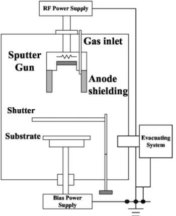
The Sn thin films were prepared by radio frequency共rf兲 magne-tron sputtering and deposited on p-type Si共100兲 wafers or stainless steel substrates using a 2-in.-diam pure Sn共99.99%兲 target. Figure 1 shows the setup of our sputter system. The dimensions of the addi-tional anode shielding have been shown in a previous paper.16The rf gun power was 40 W. The distance between target and substrate was 8.5 cm. The working gas for deposition was Ar共99.99% purity兲, and total gas flow was set at 15 sccm during sputtering. The working pressure was maintained at 1.33 Pa during deposition. By control-ling the deposition time, all Sn films described here have the same thickness of⬃120 nm, measured by an ␣-step profilometer 共Veeco Instruments, Inc., Dektak 3030ST兲. The mass of the Sn films was obtained by multiplying the mass deposition rate共mg/s cm2兲 with
deposition time. Bulk density共Sn 7.31 g/cm3兲 was assumed for the
measurement of mass deposition rates. However, because the actual film density varies with deposition conditions, the capacities 共mAh/g兲 are therefore subject to an uncertainty of ±5%.
The film crystallography was characterized by grazing-angle X-ray diffraction共XRD兲 using a Rigaku D/MAX2500 X-ray diffrac-tometer with Cu K␣ radiation 共wavelength 1.5405 Å兲. The surface morphology was observed by a JEOL JSM-6700 field emission scanning electron microscope共FESEM兲. The electrochemical tests, including charge-discharge, CV, and cycle life tests, were performed using Autolab PGSTAT30 and Jeihan 5000 potentiostat/galvanostat systems. Half-cells based on films prepared under different condi-tions were tested. Lithium metal was used as counter and reference electrodes, and the electrolyte was 1 M LiPF6and ethylene carbon-ate共EC兲 ethylmethyl carbonate 共EMC兲 共volume ratio 1:2兲 solution. The half-cells were charged共lithiated兲 and discharged 共delithiated兲 using a current of 50 and 10A cm−2共current per unit surface of
stainless steel substrate兲, respectively, with different voltage cutoff ranges, 0.05–1.00 and 0.05–2.50 V, at a constant temperature of 25°C. The larger charge current density 共50 A cm−2兲 at initial lithiated state prevents the occurrence of anomalous irreversible capacity and avoids the decomposition of electrolyte.5Typically for 120-nm-thick Sn films, the first charge took⬃2 h. The charging current of 50A cm−2corresponded to 429 mA g−1. All cells were
assembled and tested in an Ar-filled glove box. A layer of ultrathin SnO2共20 nm兲 was also deposited on top of Sn thin films using a
pure SnO2共99.99%兲 target to modulate the SEIs. The
electrochemi-cal properties of the SnO2-coated and uncoated Sn thin-film elec-trodes were studied and compared. The cells were labeled as AS
z
E-mail: kfchiu@fcu.edu.tw
Journal of The Electrochemical Society, 153共6兲 A1038-A1042 共2006兲
0013-4651/2006/153共6兲/A1038/5/$20.00 © The Electrochemical Society
共Sn thin films cycled within 0.05–2.50 V兲, AS-1 共Sn thin films cycled within 0.05–1.0 V兲, and SnO2/AS-1 共SnO2-coated Sn thin
films cycled within 0.05–1.0 V兲.
Results and Discussion
It has been reported in other literature6,17that Sn particles diffuse easily on the surface of the substrate and therefore have a strong tendency to form large clusters during deposition. However, the ad-ditional anode shielding has been shown to be an effective way to reduce the particle sizes of Sn thin films as reported in our previous work.13Figure 2 shows the surface morphology of Sn thin films deposited with the anode shielding 共labeled AS兲 sputtering tech-nique. The surface morphology of thin films are smooth and com-posed of nanosized primary particles共5–10 nm兲. The anode
shield-ing confined the plasma, resultshield-ing in lower ion flux on the substrate holder. As a consequence, Sn particles during deposition cannot gain enough energy to agglomerate and thus result in ultrasmall particle size. The AS films with SnO2surface coating also display similar morphology, as shown in Fig. 3a and b. The thickness of SnO2layer
was about 20 nm thick and the total thickness of the SnO2/AS bi-layer was about 140 nm.
Figure 4 shows the XRD patterns of AS and SnO2/AS thin films.
Both types of films exhibit low-intensity diffraction peaks and show near-amorphous features, corresponding to the nanosized surface morphologies shown in Fig. 3 and 4. The grain size共AS film in Fig. 4兲 estimated by Scherrer’s equation is around 3 nm.
Half-cells made of the Sn thin films deposited with anode shield-ing were cycled between different cutoff voltage ranges, 2.50–0.05 and 1.00–0.05 V 共labeled as AS and AS-1, respectively兲, and the composite anodes, SnO2/AS thin films, were also tested. The elec-trochemical properties and cycle life performances of these thin films are detailed in Table I and shown in Fig. 5.
As shown in Table I, the initial capacity共1248 mAh/g兲 for the cell with SnO2/AS-1 bilayers thin film is higher than the pure metal
AS-1 cell 共997 mAh/g兲 and lower than the pure SnO2 cell 共1746 mAh/g兲, as expected for a composite electrode. This means that the SnO2surface coating layer of 20 nm also contributes to the
cell capacity. Comparison of the AS, AS-1, and SnO2/AS-1 cells
Figure 1. Schematic diagram of anode-shielding-assisted magnetron sputter
system.
Figure 2. Surface morphology of deposited Sn thin films.
Figure 3. SEM images of composite SnO2/AS cells:共a兲 surface morphology and共b兲 cross section.
shows that the SnO2/AS-1 film exhibits higher irreversible capacity loss because additional lithium is consumed by the SnO2layer and
forms Li2O on the surface during the first cycle.
A relatively lower initial capacity loss of 13.11% can be obtained for the AS cells. As the cycle number increases, the capacity of the AS samples decreases. The reversible capacity decreases quickly to 522 mAh/g up to 20 cycles and then decays to 398 mAh/g after 80 cycles. Changing the cutoff voltage to 1.0 V, the AS-1 cell with the same surface morphology and the same particle size does not show the same results in cycling ability compared to AS cell. As shown in Fig. 5, the AS-1 cell shows lower capacity initially and retains higher reversible capacity than AS cell in early cycles 共569 mAh/g at cycle 20兲. However, as the cycle number exceeds 30, the reversible capacity of the AS-1 cell rapidly decays again and is as low as 257 mAh/g after 80 cycles.
The AS and AS-1 cells were prepared in the same sputtering run and assembled in the same conditions and time. However, these cells show obviously different cycling performances, as seen in Fig. 5. In the initial stage of the cycle test, the capacity retained well for the AS-1 cell compared to the AS cell. It is supposed for the AS-1 cell that variation in volume due to lithiation/delithiation processes are relatively small compared to the AS cell. However, the AS cell is cycled in a large potential range共2.50–1.00 V兲 and may undergo more severe volume changes, which can result in cracks and the loss of electric contact between Sn particles and film/substrate interfaces. Therefore, the reversible capacity of the AS cell共522 mAh/g兲 fades quickly and is lower than that of the AS-1 cell共569 mAh/g兲 in the first 20 cycles. Surprisingly, as both samples are cycled beyond 20 cycles, the capacity of the AS-1 cell decreases dramatically. It is possible that the SEI is responsible for this different performance. Figure 6a and b shows the CV curves of both cells scanned at 0.2 mV/s. We can observe the reduction peak above 1.00 V and the differences between the first sweep and subsequent sweeps in AS
and AS-1 cells. It is well known that there is no formation of LixSn
phases above 0.8 V for Sn electrodes.1,3 Hence, we suppose that there is SEI formation at around 1.37–1.50 V and that this is the critical point which affects the stability of the AS-1 cells in the cycling test. In Fig. 6a, low intensities of reduction peaks at approxi-mately 1.27 V can be still found for AS cells at the second sweep. It is the typical phenomenon for the lithium alloy anodes. The lithium alloy anodes suffer from severe volume changes and cracks at the first charge–discharge and subsequent cycles. The completion of SEI formation takes several charge–discharge cycles.18In the cracked electrode, the new electrochemically active Sn particles are exposed to the electrolyte. Consequently, more and thicker SEI layers are formed after several cycles and then help to fully cover the surface of the Sn thin film. This thick SEI serves as a flexible capping layer, which increases the integrity of the films and thus enhances the endurance of following volume changes. As a result, the AS cell shows better cycling performance and good capacity retention in long cycling tests. For the AS-1 cell, there are only mild volume changes initially. Therefore, the SEI layers are thinner and do not cover the film surface as well. As the stress accumulates after more than 20 cycles, the film severely cracks. Because the thin SEI layer is not able to hold the cracked films, film peel-off may readily occur. Figure 7a and b shows the XRD patterns of AS and AS-1 cells after 80 cycles共at 0.05 V兲. The XRD samples are prepared in an argon-filled glove box and then rinsed with electrolyte to clean the precipitates of the lithium compound formed after cycling. We can observe the near-amorphous Sn peak centred near 31° with wide full width at half-maximum 共fwhm兲 for both AS and AS-1 films as shown in Fig. 7, which corresponds to the Sn peak shown in Fig. 4. For the AS-1 film, this characteristic peak is sharper than the AS film, by comparing the fwhm values, possibly indicating that the Sn particles agglomerate after 80 cycles. For the AS cell with a well-capped SEI layer, the Sn peak shows a much lower intensity,
Table I. Electrochemical performances of the Sn thin films deposited under different conditions.a
Samples Cutoff voltage 共V兲 Initial charge capacity 共mAh/g ± 5%兲 Initial efficiency 共%兲 Discharge capacity at cycle 1 共mAh/g ± 5%兲 Discharge capacity at cycle 20 共mAh/g ± 5%兲 Discharge capacity at cycle 50 共mAh/g ± 5%兲 AS 2.50–0.05 963 86 828 522 432 AS-1 1.00–0.05 997 65 624 569 335 SnO2/AS-1 1.00–0.05 1248 46 589 570 528 SnO2a 1.00–0.05 1746 38 663 — —
aThis cell is for comparison, and no cycling test was performed.
Figure 4. XRD patterns of AS and composite SnO2/AS thin films.
Figure 5. Cycling tests of AS, AS-1, SnO2/AS-1 cells.
A1040 Journal of The Electrochemical Society, 153共6兲 A1038-A1042 共2006兲
indicating that the thicker SEI layer of the AS film may buffer the Sn particles and therefore prevent the agglomeration on the film surface.
Both films show characteristic peaks of LixSn alloys, as seen in Fig. 7a and b. For the AS film, the diffraction peaks corresponding to Li2.6Sn, Li3.5Sn, and Li4.4Sn are detected. However, for AS-1 film,
only highly lithiated peaks, Li3.5Sn and Li4.4Sn, are detected. This
indicates that the lithiation degree of the AS film is lower than the AS-1 film, because low lithium content phase Li2.6Sn is detected only in the AS film. These results may be attributed to the well-capped SEI layer for the AS film, which hinders the transportation of Li ions and reduces the degree of lithiation.
However, it is difficult to identify the structure and electrochemi-cal properties of a SEI layer. Therefore, the deliberately deposited ultrathin SnO2layer may serve as an artificial SEI layer. Interest-ingly, the SnO2/AS-1 cell shows the best cycling ability among the
three cells. Despite the fact that it is also cycled in the cutoff voltage range of 0.05–1.00 V, the SnO2/AS-1 cell shows the highest
revers-ible capacity. After the initial capacity loss reversrevers-ible capacity of ⬃589 mAh/g with near 100% capacity retention can be achieved for up to 20 cycles, and it still has a capacity of over 450 mAh/g after 80 cycles.
As reported in the literature,13,14the amorphous Li2O 共a-Li2O兲
can be well-formed and held under 1.3 V for the SnO2films. It is possible that this a-Li2O SEI and the remaining SnO2 serve as a
protection layer, stabilizing the AS-1 cell. As a result, the cell can endure or prevent cracking and crumbling. It also stops the active Sn thin films from reacting with the electrolyte. The well-capped SnO2/AS-1 cells show much better capacity retention than AS-1
cells, and in fact, the highest capacity retention up to 80 cycles among the tested cells. Hence, we can conclude that the cycling
performance of Sn thin-film electrodes may be improved effectively by using a suitable charge–discharge scheme or by coating a suitable capping layer共i.e., passivation layer兲.
Conclusions
Nanosized Sn thin films were deposited using rf sputter deposi-tion with addideposi-tional anode shielding equipped on the sputter gun. It has been demonstrated that producing an appropriate SEI protection layer, by cycling in the 2.50–0.05 V range, or depositing a surface capping layer can effectively improve the cycling properties. For Sn films with a smooth and fine surface under a well-capped SnO2
layer, reversible capacity can be significantly improved.
Acknowledgments
This research work was sponsored by Taiwan R.O.C. National Science Council under contract no. NSC 92-2216-E-035-024 and NSC 93-2216-E-035-024.
Feng Chia University assisted in meeting the publication costs of this article.
References
1. M. Winter and J. O. Besenhard, Electrochim. Acta, 45, 31共1999兲. 2. J. Yang, M. Winter, and J. O. Besenhard, Solid State Ionics, 90, 281共1996兲. 3. R. A. Huggins, J. Power Sources, 81/82, 13共1999兲.
4. L. Y. Beaulieu, S. D. Beattie, T. D. Hatchard, and J. R. Dahn, J. Electrochem. Soc.,
150, A419共2003兲.
5. S. D. Beattie, T. D. Hatchard, A. Bonakdarpour, K. C. Hewitt, and J. R. Dahn, J.
Electrochem. Soc., 150, A701共2003兲.
6. L. Y. Beaulieu, T. D. Hatchard, A. Bonakdarpour, M. D. Fleischauer, and J. R. Dahn, J. Electrochem. Soc., 150, A1457共2003兲.
7. J. O. Besenhard, J. Yang, and M. Winter, Abstracts of the 8th International Meeting
on Li Batteries, Nagoya, Japan, p. 96共1996兲.
8. O. Mao, R. L. Turner, I. A. Courtney, B. D. Fredericksen, M. I. Buckett, L. J.
Figure 6. CVs of the sputtered Sn thin films swept between共a兲 2.50–0.05
and共b兲 1.00–0.05 V 共scan rate 0.20 mV s−1兲.
Figure 7. XRD patterns of Sn thin films after 80 cycles between 共a兲
2.50–0.05 V共AS兲 and 共b兲 1.00–0.05 V 共AS-1兲. The films were fully charged 共lithiated兲 to 0.05 V.
Krause, and R. J. Dahn, Electrochem. Solid-State Lett., 2, 3共1999兲. 9. K. Ogisu, Portable Power 2005 Conference, San Francisco, CA共2005兲. 10. E. Peled, J. Electrochem. Soc., 126, 2047共1979兲.
11. E. Peled, in Lithium Batteries, J.-P. Gabano, Editor, p. 43, Academic Press, New York共1983兲.
12. I. A. Courtney and J. R. Dahn, J. Electrochem. Soc., 144, 2045共1997兲. 13. I. A. Courtney and J. R. Dahn, J. Electrochem. Soc., 144, 2943共1997兲. 14. Y. Idota, T. Kubota, A. Matsufuji, Y. Maekawa, and T. Miyasaka, Science, 276,
1395共1997兲.
15. T. J. Kim, D. Son, J. Cho, B. Park, and H. Yang, Electrochim. Acta, 49, 4405
共2004兲.
16. K.-F. Chiu, H. C. Lin, K. M. Lin, T. Y. Lin, and D. T. Shieh, J. Electrochem. Soc., Submitted共2005兲.
17. L. Y. Beaulieu, K. C. Hewitt, R. L. Turner, A. Bonakdarpour, A. A. Abdo, L. Christensen, K. W. Eberman, L. J. Krause, and J. R. Dahn, J. Electrochem. Soc.,
150, A149共2003兲.
18. K. Zaghib, K. Tatsumi, H. Abe, H. Sakaebi, S. Higuchi, T. Ohsaki, and Y. Sawada, Abstract 581, The Electrochemical Society Meeting Abstracts, Vol. 94-1, San Fran-sisco, CA, May 22–27, 1994.
A1042 Journal of The Electrochemical Society, 153共6兲 A1038-A1042 共2006兲