Oxadiazole Derivatives Used as the Host of the Metal Doped Electron
Transport Layer Material
Hsu-Tun Teng
a, Meng-Hsiu Wu
a, Jiun-Haw Lee
*a, Chun-Chieh Chao
b, Hung-Lin Chen
b, and
Man-Kit Leung
ba
Graduate Institute of Electro-Optical Engineering and Department of Electrical Engineering,
National Taiwan University, No. 1, Sec. 4, Roosevelt Road, Taipei, Taiwan, R.O.C.;
b
Department of Chemistry, National Taiwan University, Taipei, Taiwan, R.O.C
ABSTRACT
In this paper, we demonstrate device performances with cesium (Cs) doped in oxadiazole (OXD) derivatives as a metal-doped electron transport layer (MD-ETL). Cs is a heavy alkali atom and difficult to diffuse in an organic matrix. The metal quenching effect is therefore reduced in a long-term operation. Three different kinds of OXD-based organic materials were used. However, only one kind of OXDs can effectively improve the device performances. Such a host material exhibits advantages of high glass transition temperature (Tg) of 147 oC. The average roughness of the thin film is small hence the leakage current of the corresponding OLED devices is low. By using a highly reflective and conductive silver cathode, an OLED with a 2.59 V reduction in driving voltage, a 47.3% increase in current efficiency, and a 3.14 times enhancement in operation lifetime was demonstrated.
Keywords: OLED, conductivity, ETL.
1. INTRODUCTION
Organic light-emitting displays (OLED) have recently attracted much attention because of the advantages of low-power consumption, high brightness, high contrast, and low cost [1],[2]. However, high driving voltage and short operation lifetime are major limitations for the current OLED devices in applications as compared to other competitive display technologies such as semiconductor light-emitting diodes (LEDs) and liquid crystal displays (LCDs).
In order to break through these limitations, organic materials having high conductivity and good electrical contact with electrodes are desired. Recently, doping techniques, which have been widely used in forming inorganic semiconductors, have been applied for forming organic p- and n-type materials [3]. Although efficient p-type doping is possible for a variety of organic materials, examples based on the n-type doping with high stability are rare [4]. A typical
n-type doping electron transport layer (ETL) consists of a low work-function metal doped in an organic material.
Co-evaporation of the materials, which is called the metal-doped (MD) technique, is commonly employed for preparing
H3E
BCP
this ETL [5]. Although lithium was found to be one of the most efficient dopants, it would easily diffuse into the light-emitting layer (EML) and hence induce the metal ion quenching effect. In a long-term operation, the current efficiency and the lifetime of the devices significantly decrease. 2,9-Dimethyl-4,7-diphenyl-1,10-phenanthrolin (BCP) and 4,7-diphenyl-1,10-phenanthroline (BPhen) are common materials for the host organic materials in MD-ETL. Their molecular structures are shown in Fig. 1. Nevertheless, their low glass-transition temperatures (Tg) of 83 and 62 oC limit the operation lifetime of the devices [6]. Co-evaporating high Tg materials such as Balq (Tg:92 oC) with Li:BPhen to form a mixed ETL does increase the operation lifetime. Unfortunately, in the case, the driving voltage increased. There seems to be a tradeoff between operation lifetime and driving voltage in this system.
OXD-1 OXD-2
OXD-3
Fig. 1 Molecular structures of different OXDs and BCP.
the ETL matrix.
The family of oxadiazole (OXD) compounds has been extensively used as electron transporting materials [7]. We are interested in developing OLED devices based on this family for several reasons: (1) The coordination-ability of 1,3,4-oxadiazoles, including the oxygen and nitrogen atoms, with Cs should be reasonably good, allowing the Cs atoms to be dispersed evenly into the organic matrix. [8] (2) The electron mobility in OXD matrix is high. [7] (3) The lowest unoccupied molecular orbital level of OXD is close to the host of our EML, tris-(8-hydroxyquinoline) aluminum (Alq3) [9] This makes the electron drifting from ETL to EML easier. This may also lead to a decrease in the driving voltage and an increase in the current efficiency.
The host material OXD-1 is a newly designed organic material with good thermal stability and high Tg of 147oC. Careful study revealed that OXD-1 and OXD-3 could form an ultra flat thin-film with a mean roughness less than 1 nm through thermal evaporation and deposition in high vacuum. On the other hand, the average roughness of OXD-2 is over 100 nm. The high mean roughness value results in high leakage current, low current efficiency, and short operation lifetime in an OLED. Due to the formation of the flat surface, the glassy OXD-1 MD-ETL can form ohmic contact with the cathode materials, including Ag and Al, regardless of the work function.
2. EXPERIMENTS
In all of the following experiments, we used ITO glass substrates with low sheet resistivity (10 Ohm/sqr) and flat surface roughness (Ra < 1 nm). The size of the active region in our test pixel is 0.5 cm x 0.5 cm. In our devices, we used
N,N’-diphenyl-N,N’-bis(1-napthyl)-1,1’-biphenyl-4,4’-diamine (NPB) as the hole-transport layer (HTL) material, and
tris-(8-hydroxyquinoline)aluminum (Alq3) as the EML. In our control device, Alq3 was used as the ETL and LiF of 1.2 nm in thickness was used as the electron injection layer between the ETL and the Al cathode. In our MD-OLEDs, we used Cs as the dopant and BCP, OXD-1, and OXD-2 as the host materials of the ETL. As mentioned above, OXD-3 exhibits a high mean roughness level and is not suitable for thin-film device. The metal dopant concentration, which is optimized as shown in ref. [10], is 10%, 20% 50% and 50 % respectively in molar ratio for BCP, OXD-1, OXD-2 and OXD-3. The thickness of the Al and Ag cathode were 100 nm. Figure 2 illustrates the layer structures. After organic and metal deposition, we encapsulated in the glove box with O2 and H2O concentrations below 1 ppm. Prior to the lifetime
test, devices were characterized with a Keithley 2400 source meter for current-voltage measurement and with a PR-705 photometer for the brightness measurement. In our lifetime test, we fixed the initial luminance at 10000 cd/m2 and supplied a constant current to our devices. The brightness and voltage were recorded with a PR-705 photometer and a Keithley 2400 source-meter at different durations.
Fig. 2 Device structures of the OLEDs.
3. RESULTS AND DISCUSSIONS
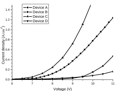
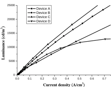
Current density versus voltage (J-V) and current efficiency versus current density (η-J) comparison among the four devices are shown in Fig. 3 and Fig. 4, respectively. Device A is the conventional device with the current density and the current efficiency of 0.1 A/cm2 and 3.35 cd/A at 9.72 V which is a typical value in such a device. Since Ag has a lower optical absorption and higher electrical conductivity than Al, such a replacement could effectively improve device performance. When we change the ETL from Alq3 to Cs:BCP and replace the Al cathode by an Ag cathode (device B), the driving voltage is reduced by 1.86 V and the current efficiency was increased by 29 % at a current density of 0.1 A/cm2. In an NPB/Alq3 device, holes in NPB exhibit higher mobility than electrons in Alq3 [11]. That means the electric field in ETL is higher than that in HTL. Such a carrier unbalance results in a lower recombination rate and lower current efficiency [12]. Introducing the MD technology in the device design does not only decrease the driving voltage but also improves the electron-hole balance. This explains the higher current efficiency in our MD-OLED. When we changed the host material of the EML from BCP to bis-OXD with an Ag cathode, the driving voltage and the current efficiency reach 4.93 cd/A and 7.32 V, respectively at the same current density. We can see that, the driving voltage was lower in device C than device B. The LUMO energy levels of 1.8, 2.17, and 3.7 eV for BCP, OXD-1, and Alq3 were measured
Device HTL EML ETL Cathode
55 nm 27.5 nm 27.5 nm 100 nm A Alq3 LiF/Al B Cs:BCP Ag C Cs:OXD-1 Ag D NPB Alq3 Cs:OXD-3 Ag
However, when using OXD-2 as the host of the EML, the driving voltage is 10 V at 0.1 A/cm2 with a current efficiency of 3.3 cd/A. The voltage is higher and the current efficiency is lower in such a device. That means not all OXD derivatives can be used as the host materials of the MD-ETL. A suitable material design is necessary for this purpose. More experiments will be done to study the reaction mechanisms between the Cs and the OXDs.
6 7 8 9 10 11 0.0 0.2 0.4 0.6 0.8 1.0 1.2 1.4 C u rr e n t de nsi ty ( A/ cm 2 ) Voltage (V) Device A Device B Device C Device D
0.0 0.1 0.2 0.3 0.4 0.5 0.6 0.7 0 5000 10000 15000 20000 25000 Lu m in a n c e ( cd /m 2 )
Current density (A/cm2)
Device A Device B Device C Device D
Fig. 4 Comparison of brightness versus current curves.
Figure 5 shows the results of the accelerated operation-lifetime tests of devices A, B and C. Ones can see that our control device, device A, has the shortest lifetime. The extrapolated half lifetime under the brightness of 10000 cd/m2 is 13.6 hours. Device B exhibits a half lifetime of 24 hours, despite the lower Tg of the metal-dopant/host matrix. Two possible reasons may explain this phenomenon. The first is the higher power efficiency of the MD devices which generate less heat during operation. The second is the lower diffusion rate of Cs, which is used as the dopant in the OLED devices. This leads to less quench effect. For device C containing Cs:OXD as the MD-ETL layer, the operation lifetime is as high as 42.5 hours. This is 146% and 213% longer than those for the Cs:BCP and control devices respectively. Although the reasons behind this are unconfirmed, the high Tg characteristics of OXD may play an important role in the high efficiency and the long operation lifetime.
Fig. 5 Accelerated lifetime test of devices.
4. SUMMARY
In summary, we have shown novel high performance OLED devices based on MD-ETL and cathode materials. These could effectively decrease the driving voltage of the device and increase the current efficiency and operation lifetime. A suitable molecule design is needed for the host of the MD-ETL. Ag was used as the cathode electrode to lower the ohmic loss and reduce the optical absorption. We chose Cs as the dopant material in the ETL to decrease the effects of metal ion diffusion, and inhibit the quenching effects in a long-term operation. For devices with MD-ETL, not only the driving voltage was decreased, higher current efficiency was also achieved due to better charge balance. Perhaps due to the high thermal stability and good energy alignment with EML, the lifetime of the devices based on Cs doped OXD ETL increased.
REFERENCES
1. C. W. Tang and S. A. Vanslyke, Appl. Phys. Lett. 51, 913 (1987). 2. C. W. Tang and S. A. Vanslyke, J. Appl. Phys. 65, 3610 (1989).
3. J. Huang, M. Pfeiffer, A. Werner, J. Blochwitz, S. Liu, and K. Leo, Appl. Phys. Lett. 80, 139 (2002). 4. S. T. Lee and Z. Q. Gao, and L. S. Hung, Appl. Phys. Lett. 75, 1404 (1999).
5. J. Kido and T. Matsumoto, Appl. Phys. Lett. 73, 2866 (1998).
6. B. W. D'Andrade, S. R. Forrest, and A. B. Chwang, Appl. Phys. Lett. 83, 3858 (2003).
7. S. Oyston, C. Wang, G. Hughes, A. S. Batsanov, I. F. Perepichka, M. R. Bryce, J. H. Ahn, C. Pearson, and M. C. Petty, J. Mater. Chem. 15, 194 (2005).
0 10 20 30 40 5000 6000 7000 8000 9000 10000 Lu mi n a nce ( cd/m 2 ) Time (hours) Device C Device B Device A
8. J. F. Wang, G. E. Jabbour, E. A. Mash, J. Anderson, Y. Zhang, P. A. Lee, N. R. Armstrong, N. Peyghambarian, and B. Kippelen, Adv. Mater. 11, 1266 (1999).
9. Y. Kawabe and J. Abe, Appl. Phys. Lett. 81, 493, (2002)
10. J. H. Lee, M. H. Wu, and C. C. Shiau, Taiwan Display Conferences, Taipei, Taiwan, 10-11 June (2004). 11. W. Brütting, S. Berleb and A. G. Mückl, Org. Electron. 2, 1 (2001).