Optical properties of self-assembled ZnTe quantum dots grown by molecular-beam
epitaxy
C. S. Yang, Y. J. Lai, W. C. Chou, W. K. Chen, M. C. Lee, M. C. Kuo, J. Lee, J. L. Shen, D. J. Jang, and Y. C. Cheng
Citation: Journal of Applied Physics 97, 033514 (2005); doi: 10.1063/1.1834985 View online: http://dx.doi.org/10.1063/1.1834985
View Table of Contents: http://scitation.aip.org/content/aip/journal/jap/97/3?ver=pdfcov
Published by the AIP Publishing
Articles you may be interested in
Self-assembled ZnO quantum dots with tunable optical properties
Appl. Phys. Lett. 89, 023122 (2006); 10.1063/1.2221892
Enhanced photoluminescence of InAs self-assembled quantum dots grown by molecular-beam epitaxy using a “nucleation-augmented” method
Appl. Phys. Lett. 85, 567 (2004); 10.1063/1.1773914
Formation mechanism of CdTe self-assembled quantum dots embedded into ZnTe barriers
Appl. Phys. Lett. 81, 993 (2002); 10.1063/1.1477280
Optical properties of ZnMgSeTe quaternary alloys grown on ZnTe substrates by molecular-beam epitaxy
J. Vac. Sci. Technol. B 18, 1530 (2000); 10.1116/1.591420
Photoluminescence study of CdTe/ZnTe self-assembled quantum dots
Appl. Phys. Lett. 74, 3011 (1999); 10.1063/1.123996
Optical properties of self-assembled ZnTe quantum dots grown
by molecular-beam epitaxy
C. S. Yang, Y. J. Lai, W. C. Chou,a) W. K. Chen, and M. C. Lee
Department of Electrophysics, National Chiao Tung University, Hsin-Chu, Taiwan 30010, Republic of China
M. C. Kuo, J. Lee, and J. L. Shen
Department of Physics, Chung Yuan Christian University, Chung-Li, Taiwan 32023, Republic of China
D. J. Jang
Department of Physics, National Sun Yat-sen University, Kaohsiung, Taiwan 804, Republic of China
Y. C. Cheng
Material and Electro-Optics Division, Chung-Shan Institute of Science and Technology, Lung-Tan, Taoyuan, Taiwan 325, Republic of China
(Received 21 May 2004; accepted 25 October 2004; published online 6 January 2005)
The morphology and the size-dependent photoluminescence (PL) spectra of the type-II ZnTe quantum dots(QDs) grown in a ZnSe matrix were obtained. The coverage of ZnTe varied from 2.5 to 3.5 monolayers(MLs). The PL peak energy decreased as the dot size increased. Excitation power and temperature-dependent PL spectra are used to characterize the optical properties of the ZnTe quantum dots. For 2.5- and 3.0-ML samples, the PL peak energy decreased monotonically as the temperature increased. However, for the 3.5-ML sample, the PL peak energy was initially blueshifted and then redshifted as the temperature increased above 40 K. Carrier thermalization and carrier transfer between QDs are used to explain the experimental data. A model of temperature-dependent linewidth broadening is employed to fit the high-temperature data. The activation energy, which was found by the simple PL intensity quenching model, of the 2.5, 3.0, and 3.5 MLs were determined to be 6.35, 9.40, and 18.87 meV, respectively. © 2005 American Institute of Physics.[DOI: 10.1063/1.1834985]
INTRODUCTION
The fabrication of quantum-dot (QD)-based light-emitting devices encounter several problems. Reducing the threshold current and voltage, increasing the quantum effi-ciency, and prolonging the lifetime of the devices remain challenges.1–3 Photoluminescence (PL) spectroscopy is a powerful method for characterizing the optical properties of the QD system, which is essential to solve some of the above problems. The temperature-dependent PL spectra for both III-V and II-VI compound semiconductor QDs were studied in detail to examine the temperature stability and the funda-mental light-emission mechanisms. The temperature-dependent PL spectra of QD systems have several pro-nounced signatures. (i) For a single QD, the temperature-dependent PL linewidth broadening follows the theoretical linewidth broadening model. However, for an ensemble QD, the line narrows initially at low temperatures and then fol-lows the theoretical model and broadens at higher temperatures.4(ii) A strong redshift in energy with increasing temperature was observed.4,5(iii) The PL intensity increased with temperature first at low temperatures and then declined as the temperature was increased further.5–7The above phe-nomena could be explained by a steady-state model for the carrier dynamics which takes into account the distribution of
the quantum dot size and random population effects, and carrier capture, relaxation, and retrapping.8 In the current study, excitation power and temperature-dependent photolu-minescence spectra are used to characterize the optical prop-erties of the ZnTe quantum dots, which were grown in a ZnSe matrix for possible application in optoelectronic de-vices. The band alignment of the ZnTe/ ZnSe QD system is type II.9 The emission mechanism differs from that of the well-known InAs/ GaAs type-I QD system.
EXPERIMENTS
Self-assembled ZnTe QDs were grown in a ZnSe matrix on the epiready semi-insulated GaAs substrate using a Riber 32P molecular-beam epitaxy (MBE) system. Initially, the GaAs substrate was desorbed at 580 ° C in the III-V chamber and then the GaAs buffer layer of 0.2m was deposited. The desorption and growth processes were monitored via the reflection high-energy electron diffraction(RHEED) pattern. After the GaAs buffer was grown, the substrate was trans-ferred to the II-VI chamber to grow the ZnTe QD structure. The substrate temperature 共TS兲 was raised to 400 °C, at
which it remained for about 10 min. Then, TSwas reduced to
280 ° C to grow the ZnSe buffer layer. The ZnSe buffer layer included several monolayers (MLs) grown by migration-enhanced epitaxy10 and a thickness of 50 nm grown by con-ventional MBE. The average roughness of the ZnSe buffer layer was approximately 0.5 nm, indicating that the surface a)Author to whom correspondence should be addressed; electronic mail:
JOURNAL OF APPLIED PHYSICS 97, 033514(2005)
0021-8979/2005/97(3)/033514/7/$22.50 97, 033514-1 © 2005 American Institute of Physics
of the ZnSe buffer layer is flat. After the flat ZnSe buffer layer was deposited, the growth of the self-assembled ZnTe QDs was begun. The growth rate of the ZnTe dots was about 5.2 MLs/ min. The average coverage of ZnTe for samples one to five was 2.0, 2.5, 3.0, 3.5, and 4.0 MLs, respectively. Two sets of samples were grown. The first set was grown for PL measurement. A ZnSe capping layer of about 50 nm was grown following the growth of the ZnTe dots. The other set of samples grown without a ZnSe capping layer was used for atomic force microscopy(AFM) study. The NT-MDT Solver P47 AFM was used to examine the morphology. Measure-ments were made in the semicontact mode. The scan steps in the x and y directions were both 4.8 nm. The resolution was 0.01 nm in the z direction. The 325-nm line of a He–Cd laser
共55 mW兲 was used to excite the PL spectra. While a GaN
diode laser共396 nm兲 was used to be the pumping source for the power-dependent PL measurement. The samples were mounted on the cold finger of a closed-cycle refrigerator, whose temperature was controlled between 10 and 300 K. A Spex 1403 double-grating spectrometer equipped with a ther-mal electric cooled photomultiplier tube was used to analyze the PL spectra. Slit widths were set to 100m to yield a spectral resolution better than 0.1 meV.
RESULTS AND DISCUSSION
Figure 1 shows the atomic force microscopic images of the ZnTe quantum dots with an average ZnTe coverage of 3.0 MLs. The average dot diameter and height are 40.5 and 7.86 nm, respectively. The estimated dot density is 1.5
⫻109cm−2. For ZnTe coverage below 2.0 MLs, no quantum dots were formed. Above 4.0 MLs, the dots were too dense and the ripening growth mode occurred. The optical proper-ties of the ZnTe QDs with a coverage of more than 4.0 MLs deteriorated. Hence, in this work, the optical spectra of ZnTe QDs were limited to those of samples with ZnTe coverage of between 2.5 and 3.5 MLs.
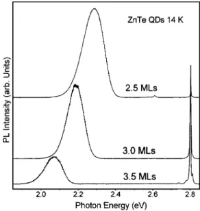
Figure 2 shows the photoluminescence spectra of the ZnTe QDs with coverage of 2.5, 3.0, and 3.5 MLs. The sharp peak near 2.8 eV is associated with the near band-edge emis-sion, free heavy- and light-hole excitons and the
impurity-bound excitons, of the ZnSe matrix.11The PL peak energies of the ZnTe QDs with coverage of 2.5, 3.0, and 3.5 MLs are at 2.282, 2.181, and 2.066 eV, respectively. The redshift in the energy with the increasing ZnTe coverage is attributed to the decrease in the quantum confinement energy as the QD size is increased, due to increased thicker ZnTe coverage. The emission energies are lower than that of the ZnTe epil-ayer(2.4 eV at 10 K), implying a type-II band alignment of the ZnTe QDs grown in the ZnSe matrix, as schematically depicted in Fig. 3 using the conduction-band and valence-band offsets of ⌬Ec= 0.6 eV and ⌬E= 1.0 eV,
respectively.12The energy from the valence-band edge to the conduction-band edge of the type-II emission is around 1.8 eV. The energy difference ⌬E between the PL peak en-ergy(2.282, 2.181, and 2.066 eV) and 1.8 eV is attributed to the confinement energy of the valence-band hole in the ZnTe QD potential well. Note that, in the CdSe/ ZnSe QD system, Xin et al.6 reported that a large energy difference 共⌬E
⬃0.5 eV兲 between the type-I CdSe QD peak energy FIG. 1. AFM plain view image of ZnTe QDs with 3.0 MLs.
FIG. 2. Photoluminescence spectra of ZnTe QDs with 2.5, 3.0, and 3.5 MLs.
FIG. 3. Schematic type-II band alignment for ZnTe QDs.
033514-2 Yanget al. J. Appl. Phys. 97, 033514(2005)
共2.3 eV兲 and the energy of the valence-band to
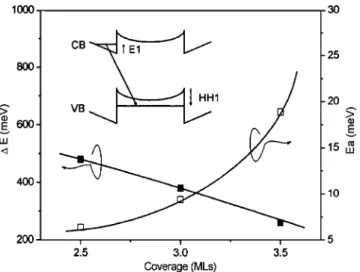
conduction-band edge(1.8 eV for cubic CdSe) is due to the interdiffu-sion of Zn and Cd atoms and the strain-induced valence-and/or conduction-band shifts. Figure 4 plots ⌬E versus ZnTe coverage: ⌬E decreases as the ZnTe coverage in-creases. The activation energy obtained from the temperature-dependent PL, which will be discussed later, is represented on the y axis on the right-hand side of the plot. The dotted and solid lines are guides to the eye.
Glaser et al.13 proposed a bent band structure, as sche-matically depicted in the insert of Fig. 4, to explain the strong PL of the InSb/ GaAs QD system. Band bending is most significant around the top of the ZnTe QD. It is caused by the electron–hole Coulomb interaction, which in turns generates the respective hole and electron potential well near the ZnTe QD and the ZnSe matrix interface. In Fig. 2, the decrease of the PL intensity as the dot size increases may be caused by the increase in the electron and hole separation with the increasing size of the ZnTe type-II QD, since the hole wave function become less confined.(The hole is fur-ther away from the top of the ZnTe QD.) However, the de-crease of the PL line integrated intensity could also be due to other effects. When the coverage increases from 2.5 to 3.5 MLs not only increase the dot size of ZnTe QDs but also induce some extended defects, which are caused by strain, relaxed or ripening growth mode occurs. Those extended de-fects usually occur on the interface between QD and matrix, and form the nonradiative center.14
Figure 5 shows the shift of the PL peak energy with the excitation power for the sample with 2.5 (square), 3.0 (tri-angle), and 3.5 MLs (circle) at 12 K. The excitation power is increased from 3 to 380W. A blueshift occurs as the exci-tation power is increased. This shift is characteristic of all type-II structures.15,16Consider the band structure in the inset in Fig. 4. A high excitation power promotes the generation of numerous electron–hole pairs, which are located in the sepa-rated region, increasing the degree of the bending band. Therefore, in the type-II structure, the electron–hole pair re-combination energy increases with the excitation power. The
energy shifts of the 2.5-, 3.0-, and 3.5-ML samples are 11, 12, and 6 meV, respectively. The dot sizes cause the varia-tion in energy shifts. The sample with 3.5 MLs has larger dots than the samples with 2.5 and 3.0 MLs, indicating the lower confinement energy of the hole. This result implies that band bending is suppressed and transition energy is de-creased.
Figures 6(a)–6(c) show the temperature-dependent PL spectra of the 2.5-, 3.0-, and 3.5-ML samples. Four important issues must be considered:(i) temperature-dependent energy shifts, (ii) the line broadening with temperature, (iii) temperature-dependent intensity, and (iv) activation energy, which characterizes the temperature stability of the material system. They are discussed below.
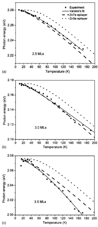
The PL peak energies of the 2.5- and 3.0-ML samples decrease monotonically as the temperature increases. The redshift in energy is attributed to the shrinkage of the band gap as the temperature increases. Figure 7 summarizes the peak energies. Varshni’s equation,17 as shown below, was employed to fit the experimental data.
Eg共T兲 = Eg共0兲 −
␣T2
共T +兲, 共1兲
where Eg共T兲 and Eg共0兲 are the band gap at temperatures T
and 0 K, and␣andare fitting parameters that are charac-teristic of a given material. For comparison, the dotted and dashed lines are Varshni’s fits of the temperature-dependent band gap for the ZnSe and ZnTe epilayers, respectively. The PL peak positions of the samples with 2.5 and 3.0 MLs fol-low the temperature-dependent band gap of the ZnTe epil-ayer rather than that of the ZnSe epilepil-ayer, since the temperature-dependent band-gap redshift is more pro-nounced for ZnTe. However, the PL peak energy for the
FIG. 4. Energy difference共⌬E兲 between the PL peak energy (2.282, 2.181, 2.066, and 1.958 eV) and 1.8 eV and activation energy共Ea兲 vs ZnTe
cov-erage. The insert depicts a bent band structure.
FIG. 5. The shift of PL peak energy with excitation power for the 2.5-, 3.0-, and 3.5-ML samples at 12 K. The excitation power is increased from 3 to 380W.
033514-3 Yanget al. J. Appl. Phys. 97, 033514(2005)
sample with 3.5 MLs is initially blueshifted as the tempera-ture increases to around 40 K, and then redshifted as the temperature increases further. A blueshift of about 10 meV is clearly observed for the 3.5-ML sample at low temperature. A strong redshift in energy, which is a signature of carrier transfer from the smaller QDs(higher energy states) to the larger QDs (lower energy states), is also observed at high temperature (above 100 K). The redshift is about 0.50 meV/ K for QD and is much larger than that of the ZnTe epilayer which is approximately 0.35 meV/ K. Funato
et al.7 proposed a potential fluctuation model, as shown in Fig. 8, to explain the initial energy blueshift of the MgS / CdSe QD system. In Fig. 8(a), the regions marked I
(I
⬘
) and II (II⬘
) are the CdSe islands (which correspond tothe ZnTe QDs in this work) while region III is either the CdSe wetting layer or the MgS barrier layer(corresponding to the ZnTe wetting layer or the ZnSe layer). At a low tem-perature of 10 K, holes are confined in the localized I states. The PL structure is dominated by the emission from the lo-calized I state. As temperature is increased slightly, the holes are thermalized to region-II states. A blueshift in energy is then obtained. As the temperature increases further, carriers
FIG. 6. Temperature-dependent PL spectra of the 2.5-, 3.0-, and 3.5-ML samples.
FIG. 7. PL peak energy as a function of temperature for the 2.5-, 3.0-, and 3.5-ML samples. The solid line, the dashed line and the dotted line represent the fitting of Varshni’s law for the ZnTe QD, the ZnTe epilayer, and the ZnSe epilayer, respectively.
033514-4 Yanget al. J. Appl. Phys. 97, 033514(2005)
(mainly holes) transfer to the nearby local potential
mini-mums, which are the I
⬘
and II⬘
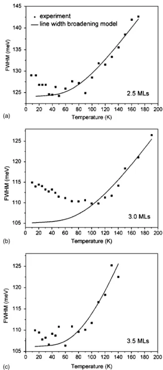
states. Therefore, the PL peak is strongly redshifted at a temperature of about 100 K. For the 2.5- and 3.0-ML samples, because the ZnTe coverage is less, the dot sizes are more uniform, as shown in Fig. 8(b). Only carrier transfer from the I state to the I’ state, the energy redshift, is observed. The II and II’ states do not exist, and the carrier thermalization, which is the blueshift at low tem-perature from state I to state II, does not occur.In Fig. 6, for the 2.5- and 3.0-ML samples, the line is initially narrowed at low temperature and then is broadened at a higher temperature. However, for the 3.5-ML sample, the narrowing of the linewidth at low temperature is less pronounced. The full width at half maximum (FWHM) is summarized in Fig. 9. For the 2.5- and 3.0-ML samples, line narrowing of about 5 meV is observed at low temperatures—from 10 to 50 K and from 10 to 100 K, re-spectively. While for the 3.5-ML sample, due to a weaker PL intensity, the data points fluctuated and linewidth narrowing was less clear to be observed. The narrowing of the PL line at low temperature can also be understood as involving the carrier transfer from the I state to the I’ state, as depicted in Fig. 8(b). At temperatures above 100 K, the line broadening is governed by(electron/hole)–phonon coupling and can be described by the temperature-dependent linewidth broaden-ing model,18 which is described by the following equation:
⌫共T兲 = ⌫0+⌫aT +
⌫LO1 exp共បLO1/kT兲 − 1
+⌫iexp共− 具Eb典/kT兲, 共2兲
where⌫共T兲 and ⌫0are the linewidths at temperatures T and 10 K, respectively; ⌫a is a coefficient of the exciton–
acoustic-phonon interaction, and ⌫LO is a fitting parameter which reflects the strength of the exciton–longitudinal-optical (LO)-phonon interaction. បLO1 represents the LO phonon energies for the ZnTe epilayers.19⌫iis a proportion-ality factor, which accounts for the density of the impurity center, and具Eb典 is the binding energy averaged over all
pos-sible impurities. The solid lines in Fig. 9 are obtained by using Eq.(2).
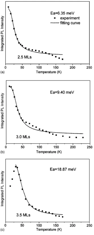
In Fig. 6, the PL intensity of the 2.5- and 3.0-ML samples monotonically decreases as the temperature in-creases. However, the PL intensity of the 3.5 ML sample first increases and decreases monotonically as the temperature rises above 40 K. Figure 10 summarizes the integrated PL intensity. The monotonic decrease with rising temperature can be described by the solid lines, which are fitted theoreti-cally using the PL intensity quenching model20 represented by the following equation:
I0共T兲 =
I0共0兲 1 + D exp共− Ea/kT兲
, 共3兲
where T is the temperature, k is the Boltzmann constant, D is a fitting constant, I0共T兲 and I0共0兲 are the integrated PL
inten-FIG. 8. Schematic potential fluctuation model(Ref. 7).
FIG. 9. FWHM of PL peak as a function of temperature for the 2.5-, 3.0-, and 3.5-ML samples. The solid lines are fitted using the line broadening model.
033514-5 Yanget al. J. Appl. Phys. 97, 033514(2005)
sities at temperatures T and 0 K, and Ea is the activation energy. The activation energies for the 2.5-, 3.0-, and 3.5-ML samples obtained by theoretical fitting are 6.35, 9.40, and 18.87 meV, respectively. The activation energy increases with the ZnTe coverage, as shown in Fig. 4. The obtained activation energies are much lower than that of the type-I QD system.21,22For the 3.5-ML sample, the integrated PL inten-sity increased then decreased maybe because the recombina-tion in the II state is quicker than that in the I state(Fig. 8). At low temperature, as the temperature is raised, the carriers
are thermalized from the localized I states into the II states. Therefore, the PL intensity increases with temperature. As the temperature is increased further, most carriers are trans-ferred into the I
⬘
and II⬘
states. The PL intensity decreases as temperature increases because the(electron/hole)–phonon interaction is gradually enhanced.CONCLUSION
In summary, the size-dependent PL spectra of type-II ZnTe QDs grown in a ZnSe matrix are obtained. The PL peak energy is found to decrease as the dot size becomes larger. A blueshift occurs as the excitation power is in-creased. The temperature-dependent PL spectra reveal a strong redshift in energy as the temperature is increased, the narrowing of the line at low temperature, and the increase in the PL intensity with (low) temperature. Carrier thermaliza-tion and carrier transfer between QDs are used to explain the experimental data. A temperature-dependent linewidth broadening model is employed to fit the high-temperature data. The decrease of the PL intensity as the temperature is increased is fitted by the simple PL intensity quenching model, to yield the activation energy, which increases with ZnTe coverage.
ACKNOWLEDGMENT
The authors would like to thank the National Science Council of the Republic of China, Taiwan for financially sup-porting this research under Contract Nos. NSC-92-2112-M-009-041 and NSC-92-2745-M-033-001.
1
Y. M. Park, Y. J. Park, K. M. Kim, J. C. Shin, E. K. Kim, M. H. Son, S. W. Hwang, and K. H. Yoo, Jpn. J. Appl. Phys., Part 1 41, 4375(2002). 2
J. X. Chen et al., J. Appl. Phys. 91, 6710(2002).
3
S. Ménard, J. Beerens, D. Morris, V. Aimez, J. Beauvais, and S. Fafard, J. Vac. Sci. Technol. B 20, 1501(2002).
4
J. Seufert, M. Rambach, G. Bacher, A. Forchel, M. Keim, S. Ivanov, A. Waag, and G. Landwehr, Phys. Rev. B 62, 12609(2000).
5
G. Karczewski, S. Mac’kowski, M. Kutrowski, T. Wojtowicz, and J. Kossut, Appl. Phys. Lett. 74, 3011(1999).
6
S. H. Xin, P. D. Wang, A. Yin, C. Kim, M. Dobrowolska, J. L. Merz, and J. K. Furdyna, Appl. Phys. Lett. 69, 3884(1996).
7
M. Funato, A. Balocchi, C. Bradford, K. A. Prior, and B. C. Cavenett, Appl. Phys. Lett. 80, 443(2002).
8
S. Sanguinetti, M. Henini, M. Grassi Alessi, and M. Capizzi, Phys. Rev. B
60, 8276(1999). 9
S. D. Baranovskii, U. Doerr, P. Thomas, A. Naumov, and W. Gebhardt, Phys. Rev. B 48, 17149(1993).
10
Y. Horikoshi, M. Kawashima, and H. Yamaguchi, Jpn. J. Appl. Phys., Part 2 25, L868(1986).
11
Y. Kim, S. L. Cooper, M. V. Klein, and B. T. Jonker, Appl. Phys. Lett. 62, 2387(1993).
12
Y. Rajakarunanayake et al., J. Vac. Sci. Technol. B 6, 1354(1988).
13
E. R. Glaser, B. R. Bennett, B. V. Shanabrook, and R. Magno, Appl. Phys. Lett. 68, 3614(1996).
14
M. V. Maksimov et al., Semiconductors 38, 1207(2004). 15
J. Böhrer, A. Krost, and D. Bimber, Appl. Phys. Lett. 64, 1992(1994).
16
F. Hatami et al., Appl. Phys. Lett. 67, 656(1995).
17
Y. P. Varshni, Physica(Amsterdam) 34, 149 (1967).
FIG. 10. Integrated PL intensity as a function of temperature for the 2.5-, 3.0-, and 3.5-ML samples. Solid lines are fitted using the PL intensity quenching model.
033514-6 Yanget al. J. Appl. Phys. 97, 033514(2005)
18
J. Lee, E. S. Koteles, and M. O. Vassell, Phys. Rev. B 33, 5512(1986). 19
R. K. Willardson, and A. C. Beer, Diluted Magnetic Semiconductors, Semiconductors and Semimetals Vol. 25, editors by J. K. Furdyna and J. Kossut(Academic, Boston, 1988).
20
Y. M. Yu, S. Nam, K. S. Lee, Y. D. Choi, and B. O., J. Appl. Phys. 90, 807
(2001). 21
C. M. A. Kapteyn et al., Appl. Phys. Lett. 76, 1573(2000).
22
J. S. Kim et al., J. Appl. Phys. 91, 5055(2002).
033514-7 Yanget al. J. Appl. Phys. 97, 033514(2005)