Abstract—A low-power tunable-band sub-harmonic
direct-con-version receiver covering the whole Unlicensed National Informa-tion Infrastructure band is demonstrated using 0.18- m CMOS technology. The RF band is selected by tuning varactors at the loads of the two-stage low-noise amplifier, while a wideband octet-phase generator is applied at the local oscillator (LO) port. The band tuning of both an LC tank and a transformer and the de-sign of an optimal transformer turn ratio are fully discussed in this paper. Vertical-NPN bipolar junction transistors in a standard CMOS process are used at the mixer switching core for excellent noise performance. As a result, the receiver achieves a 48/50 voltage gain and 4.5/4.8-dB noise figure with a noise corner of 70 kHz when the RF band is tuned to 5.2/5.8 GHz, respectively. The dc current consumption of the RF front-end (including the LO buffer) is 8.5 mA at a 1.8-V supply.
Index Terms—Direct-conversion receiver (DCR), low-noise
amplifier (LNA), octet phase, phase shifter, sub-harmonic mixer (SHM), vertical-NPN (V-NPN).
I. INTRODUCTION
T
HE low-noise amplifier (LNA) plays an important role in low-power, low-noise receiver design since the LNA must provide sufficient gain to suppress the noise figure (NF) of the whole receiver chain, but itself adds as little noise as possible. However, the design challenge increases dramatically under power constraints. In this paper, our application is focused on the Unlicensed National Information Infrastructure (U-NII) radio band, consisting of three frequency bands of 100 MHz each in the 5-GHz band: 5.15–5.25 GHz (for indoor use only), 5.25–5.35 GHz, and 5.725–5.825 GHz. Although the LNA has a low transconductance gain due to its low dc current, the high load resistance [high quality factor ( )] provides sufficient voltage gain for a better NF of the whole receiver at the cost of the RF bandwidth. In addition, a narrower RF bandwidth re-sults in little received noise and interference from other chan-nels or other communication systems. Thus, a tunable/switch-able narrowband LNA has better gain/noise performance thanManuscript received November 15, 2011; accepted December 03, 2011. Date of publication January 23, 2012; date of current version March 02, 2012. This work was supported by the National Science Council of Taiwan under Con-tract NSC 98-2221-E-009-033-MY3, ConCon-tract NSC 99-2221-E-009-049-MY3, and Contract NSC 98-2218-E-009-008-MY3, and by the Ministry of Education (MoE) Aim for the Top University (ATU) Program under Contract 95W803.
The authors are with the Department of Electrical Engineering, National Chiao Tung University, Hsinchu 300, Taiwan (e-mail: ccmeng@mail.nctu.edu. tw).
Digital Object Identifier 10.1109/TMTT.2011.2182657
a wideband LNA at a given power consumption. As a result, a two-stage LNA with tunable loads, including the first-stage LC tank and the second-stage transformer load, is employed in this study.
A direct-conversion receiver (DCR), i.e., zero-IF receiver, is well suited to low-power applications due to its simple circuit structure when compared to heterodyne or low-IF architectures. However, the dc offset, noise and problems are the primary issues for this system instead of the image and spu-rious problems of non-zero-IF architectures. A sub-harmonic mixer (SHM) is chosen for a low output dc offset due to the absence of local oscillator (LO) self-mixing [1]. In addition, MOS switching cores are directly replaced by vertical-NPN (V-NPN) bipolar-junction transistors (BJTs) available in a standard 0.18- m CMOS process. The BJT devices have a noise corner of below 1 kHz [2], [3]. Further, an LC filter is applied at the common emitter node to greatly improve the performance [4]. Moreover, by using both resonance inductors (at mixer LO port and the LC filter) and sub-harmonic mixing structure, the proposed SHM overcomes the low cutoff fre-quency of V-NPN BJTs and successfully operates at over three times the transistor . On the other hand, a wideband LO octet-phase signal generator is chosen to avoid tuning both RF and LO bands simultaneously.
Since the RF LNA is a tunable-band structure while the mixer and the LO generator have wideband topologies, a tunable nar-rowband sub-harmonic direct-conversion receiver (SH-DCR) is proposed to cover the whole U-NII bands for the RF band-width around 200 MHz. Fig. 1 shows the block diagram of the proposed SH-DCR, including a two-stage tunable-band LNA, in-phase/quadrature (I/Q) SHMs with V-NPN BJT switching core, I/Q variable-gain amplifiers (VGAs) and a wideband LO octet-phase generator. The design of a single-in-differential-out two-stage tunable-band LNA is fully described in Section II. Section III presents the details of the down-conversion circuits, while Section IV reports the measurement results. Conclusions are given in Section V.
II. TWO-STAGETUNABLE-BANDLNA
The impedance of a parallel LC tank with lossy inductor is
(1)
Fig. 1. Block diagram of the I/Q SH-DCR with a tunable narrowband LNA and a wideband LO generator using 0.18- m CMOS technology.
Fig. 2. Schematic of an LC tank with a lossy inductor.
Typically, the series resistance can be assumed as
, where is close to a constant, only relating to the geometrical shape (including width, spacing, and thick-ness). Thus,
(2) when , as proven in Appendix A. This is why an LC tank with a lossy inductor is commonly approximated as an RLC parallel tank, as shown in Fig. 2.
Further, in Appendix A, a more general case, stages of RLC tanks in cascade with the same , is considered for bandwidth. Thus, an -dB bandwidth can be calculated as , where , which is defined in Appendix A. If the target bandwidth boundaries are and , the required can be obtained by
(3) where the center frequency is , as also shown in Appendix A. Note that the 3-dB bandwidth of a single-stage
LC tank is by adopting .
By (3), to achieve a 3-dB bandwidth covering the whole U-NII band (5.15–5.825 GHz), the should be lower than 8.11. More strictly, if the gain flatness is required to be within 1 dB covering the whole band, the should be reduced to below 4.13. For a single-stage common-source (or cascode) LNA with RLC resonance load, the voltage gain can be simply
expressed as at the center frequency
. Generally speaking, the typical achievable value of an on-chip inductor is around 10. Thus, when compared to a wideband approach with . Over 2.4 times the (or extra 7.6-dB gain) is required to maintain the same voltage gain of the LNA or the IF VGA gain should be
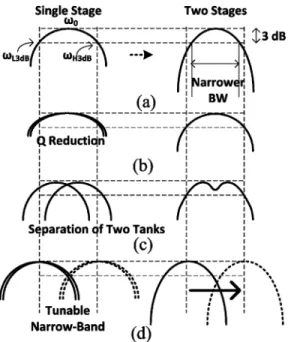
Fig. 3. (a) Frequency response of the single/two stage(s) of LC resonator(s). (b) reduction for each tank. (c) Wideband response with separation of tanks. (d) Tunable narrowband response.
increased if the NF of the RF front-end is acceptable. Either way, the power consumption is increased.
On the other hand, if multiple tanks are in cascade and located at the same frequency, the greater number of stages in cascade results in a smaller and thus a narrower bandwidth, as also de-scribed in Fig. 3(a). Either a value reduction or a separation of resonance frequencies can fulfill the original bandwidth require-ment, as illustrated in Figs. 3(b) and (c), respectively. However, gain degrades when using either method.
For the requirements of low-power, high-gain, low-noise, and RF bandwidth of 5.15–5.825 GHz in this study, a two-stage cascode LNA with a tunable RF band is chosen. A two-stage LNA is required for a sufficient gain to suppress the NF of the following SHMs at a low dc current consumption. The center frequencies of the two stages are set to be the same and vary together, as described in Fig. 3(d). Thus, a higher gain is obtained when compared with the wideband solutions, especially in a low-power condition. Since the IF bandwidth is much lower than the RF bandwidth, the frequency response of the narrow RF tank is still nearly constant within the IF bandwidth 50 MHz .
The schematic of a two-stage cascode LNA is shown in Fig. 4. An LC tank is used at the load of the first stage and a transformer at the second stage. A series inductor is sufficient for an input matching covering 5–6 GHz. Further, a gain tuning transistor is in parallel with the cascode transistor in the second stage to reduce the gain when a large RF signal is applied. Note that the gain tuning approach using tunable and fixed-bi-ased is a prototype. The cascode device can be broken into more branches with weighted sizes (not only and ), and thus a more gentle slope of the tuning curve can be achieved by digitally switching on/off the bias of each branch [5].
The frequency tuning capability of both an LC tank and a transformer load with a varactor are fully discussed as follows.
Fig. 4. Two-stage LNA with a tunable first-stage LC tank and a tunable second-stage transformer load, while a gain tuning transistor is applied in the second stage.
A. Frequency Tuning of an LC Tank
Assume the higher/lower RF bandwidth boundaries are 5.825/5.15 GHz, respectively. Thus, the first-stage
LC tank follows:
(4)
As a result,
(5)
However, where is a
con-stant capacitance including device and substrate capacitances, and is a capacitance of a varactor ranging from to . Typically, in the CMOS process, a MOS varactor
operating in an accumulation mode has a tuning ratio of 2.5. Moreover, if the varactor capacitance
ratio is defined as ,
(6) That is, should be set above 0.23 to cover the whole U-NII band. The can be changed by modifying the size of the cascode transistor, the following common-source transistor, and the dc blocking capacitance. Thus, in this study, is tuned to 0.4 pF and and are around 0.7/0.52 pF, respectively. Further,
(7) Thus, the calculated is around 1.44 nH. Finally, the used inductor in the first-stage LNA has an inductance of 1.42 nH, of 11, and of 13.5/30 GHz, respectively.
B. Frequency Tuning of a Transformer Load
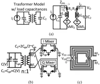
On the other hand, the second-stage LNA has a transformer load to generate differential output signals. An trans-former model is illustrated in Fig. 5(a) with the turn ratio , coupling coefficient , and
Fig. 5. (a) Transformer model with a capacitance load at the primary/ secondary coil, respectively. (b) Schematic of the LNA transformer with an input varactor and output pure capacitance load. (c) Layout construction of the 2:3 transformer.
mutual inductance . Similar to an inductor, the series resis-tance of each coil is assumed to be proportional to the series
inductance. That is, , , similar
to the inductor model.
Here, we focus on the situation of a pure capacitive load, which is especially suitable for an active mixer load. consists of the loading capacitance and the intrinsic parasitic capacitance of the transformer at each input/ output node. The transimpedance gain is considered be-cause the output current of the cascode LNA is fed to the former and then the differential output voltage is directly trans-ferred to the transconductance stage of the following ac-tive mixer, as indicated in Fig. 5(b).
Following the lumped model in Fig. 5(a), the can be ex-pressed as
(8) which is derived in Appendix B.
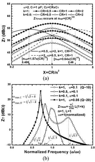
Fig. 6(a) shows the frequency response of in a nor-malized frequency condition. As shown in Fig. 6(a),
usually has two peak frequencies and
, where when of
the transformer is high. The mathematical derivation is also summarized in Appendix B. However, tends to be infinity for high coupling condition and is not suitable for real applications. Thus, is typically chosen. In addition,
the optimal turn ratio is obtained
after a thorough derivation in Appendix B if
(which is true for the two coils on the same layer with the same linewidth). Fig. 6(b) shows the at a target frequency with respect to for different input/output loading capacitance. The peak gain occurs at , as predicted.
Fig. 6. (a) Transimpedance gain of a transformer as a function of fre-quency. (b) at a target frequency with respect to for different input/output loading capacitance.
When , i.e., , the peak gain
can be simplified as
(9) The reason is also indicated in Appendix B. It is noteworthy that if , which is true especially for a stacked trans-former using two layers, shifts. Fig. 6(b) also shows that increases if , and vice versa. However, the case of
is suitable for our study.
Further, if varactors are employed at both nodes, and is still fulfilled, then
(10) which is the same as the result of a parallel LC tank because the peak frequency is proportional to tank resonance frequency
.
On the other hand, if only can be tuned, assuming , yields
(11) which is derived in Appendix C.
That is, the tuning capability of a transformer with only one varactor on either side is half of a parallel LC tank or a transformer with varactor loads at both sides. Thus, a higher should be applied to cover the desired frequency range. As shown in Fig. 5(b), mainly consists of the varactor and the of the cascode device in the second-stage LNA. Besides, at the output stage, the differential capacitances of the transcon-ductance stage of the mixers are in series, but I and Q mixers are in parallel. Therefore, the differential load capacitance is approximately equal to of a single transistor.
Similar to an LC tank, the decision of the varactor value can also be applied. Thus,
(12) Thus, should be larger than 0.417 and is set to 0.5 in this study. If is set to 0.3 pF,
pF, respectively.
pF, while pF. The
best transformer turn ratio is .
Thus, a 2:3 planar single-to-differential transformer is chosen. The layout construction of the 2:3 transformer load is shown in Fig. 5(c), while the linewidth is 9 m, line spacing is 2 m, and the outer diameter is 190 m.
III. I/Q SUB-HARMONICDOWNCONVERTER
A. SHM
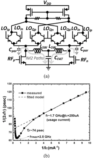
An SHM has better dc-offset output than a fundamental mixer inherently [1]. A top-LO SHM [6], [7] is applied because of a lower voltage headroom requirement and a better isolation when compared with a stacked-LO SHM at the cost of a larger LO power requirement. Additionally, parasitic V-NPN BJTs, obtained in a deep-n-well CMOS process without an extra mask [3], is applied at the mixer switching core to directly eliminate the noise problem, as shown in Fig. 7(a). Fig. 7(b) shows the as a function of of the measured data and simulated data using our fitted model with modified forward base transit time (TF) and the junction capacitance (CJC and CJE), while the dc model is provided by foundry. Besides, in this study, 0.25-mA dc current flows into one BJT transistor, and hence, the BJT only operates at around 1.7 GHz, as indi-cated in Fig. 7(b). That means a receiver covering U-NII bands (5.15–5.825 GHz) is rarely achievable originally. However, using both the sub-harmonic operation and differential reso-nance inductors, an SHM operated at three times the transistor is achieved in this study. Four differential inductors are in parallel with the base nodes of the switching core of the I/Q mixers and the output nodes of the LO generator to reduce both the conversion loss of the switching operation and the LO loss of the LO generator simultaneously. The details about the LO loss reduction will be discussed in Section III-B.
On the other hand, self-mixing, transconductor nonlinearity, switching pair nonlinearity, and mismatch in load resistors are the main reasons for the degradation in downconversion mixers [8]. Self-mixing of RF signals due to coupling into the LO port can be significantly reduced by means of layout con-cerns, e.g., metal lines carrying RF and LO signals should never
Fig. 7. (a) Top-LO sub-harmonic Gilbert mixer with V-NPN BJT in the switching core while an LC network is applied for an improvement. (b) Measured versus of the V-NPN BJT used in the mixer core emitter area m . The base transit time is around 74 ps.
cross each other, or should be kept orthogonal. Further, em-ploying highly linear polysilicon resistors makes the effect from load resistor nonlinearity negligible. Device nonlinearity of RF transconductor generates the second-order inter-modulation distortion components. A perfectly matched switching stage upconverts the input differential baseband spectrum at mixer output. However, the RF components leak into the IF output by the low-frequency gain of the switching pairs if mismatches in the switching stage devices are considered. In principle, low-frequency RF components can be filtered out by ac coupling the switching stage. However, additional power consumption resulting from biasing the input stage and mixer core separately is not desirable in our low-power application.
In this study, an LC filter is applied to filter out the current in RF transconductor [4], as shown in Fig. 7, since the shunt inductor has a relatively low impedance at low frequencies and the current can be di-rectly shorted to ground by the bypass capacitor ap-plied at the center-tapped node of the symmetric inductor. It is noteworthy that should be large enough for an im-provement. In this study, is 15 pF. When compared to the
Fig. 8. Block diagram of an LC octet-phase generator including a wideband 45 phase shifter, cross-coupled buffer amplifiers, and single-stage PPF with resonance inductors.
tens of megahertz RF applications, the value drops dramat-ically due to the parasitic capacitance at high frequencies [4]. The in the LC filter can also resonate out the parasitic . Thus, both the high-frequency gain and the perfor-mance of the Gilbert mixer can be improved.
For a chip area concern, a 3-D symmetric inductor realiza-tion is used [9]. The symmetrical 3-D inductors (effectively six turns from metal 6 to metal 1) with 8- m linewidth, 2- m line spacing, and 70- m outer diameter are applied at the LC filters in I/Q mixers and have the differential inductance of 2.4 nH and
at around 5–6 GHz.
B. Wideband LO Octet-Phase Generator
The proposed wideband octet-phase signal generator used at the LO port of the SHM, shown in Fig. 8, consists of a differen-tial-type wideband 45 phase shifter [1], [10], two differential buffer amplifiers, and two polyphase filters (PPFs) with sym-metrical inductor loads.
The LO amplitude/phase should be very accurate covering around 2.5–3 GHz (i.e., 2LO frequency of 5–6 GHz). A first-order RC phase shifter has perfect 45 phase shift only at a single frequency and a tunable version of the phase shifter using var-actors is needed. However, it is difficult to tune both RF and LO parts of the narrowband structures in a precise way for practical use. Thus, a second-order RC phase shifter is employed to cover a given bandwidth without tuning. The schematic of the phase shifter is shown in Fig. 9(a) and the RC relations are summa-rized as follows:
(13)
The output voltage of the phase shifter can be expressed as (14)
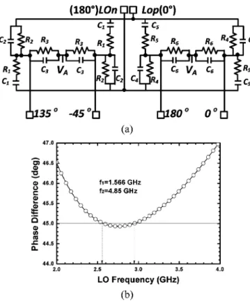
Fig. 9. (a) Schematic of a differential-type wideband 45 phase shifter. (b) Phase difference of the phase shifter with respect to frequency.
To obtain balanced amplitudes of all nodes at all frequencies, should be chosen and the voltage loss can also be expressed as
(15)
where , or .
As a result,
(16)
According to (16), the voltage loss only depends on the coef-ficient , and is independent of frequency. A smaller results in a lower loss; thus, is chosen in this study to achieve a voltage loss of 6 dB. Besides, the phase error varies as the two center frequencies and . Thus, are set at 1.566/4.85 GHz, respectively, for the perfect 45 LO phase dif-ference at 2.55 and 2.95 GHz, as shown in Fig. 9(b). Thus, ideal phase error below 0.1 is achieved covering the LO frequency from 2.5 to 3 GHz.
The amplitude/phase relationships derived above hold true when the load impedance is infinity. When a PPF is cascaded after the phase shifter for quadrature signal generation, the low input impedance of the PPF results in a significant phase error. Conversely, if the resistance is set high (e.g., over k ), i.e., the
Fig. 10. Cross-coupled differential voltage buffer applied in the LO generator.
capacitance of the PPF should be small because , the voltage loss due to the output capacitance loadings is un-acceptable [11]. As a result, an inter-stage buffer amplifier is inserted to provide a high load impedance for the phase shifter and a low source impedance for the following PPF. Parallel in-ductors resonate the capacitance including the loading mixer capacitances and PPF capacitance at to obtain a higher output impedance and reduce the PPF loss. Fig. 10 shows the schematic of the cross-coupled differential buffer amplifier [12]. The voltage gain is described as
(17) where is the transconductance of the , is the transconductance of , and is the load impedance of the following stage.
Ideally, the voltage gain is
if . When compared with a single
common-source amplifier with a diode-connected load or a common-drain amplifier, the cross-coupled amplifier has twice the voltage gain and can reduce the amplitude/phase error of the input signals. If input differential signals have amplitude imbalance and phase error, i.e., , where is a complex value near to unity. The ratio of the differential outputs is expressed as
if (18)
That is, the output voltages are perfectly differential if even though the input signals have certain amplitude/phase mismatches.
As mentioned, the capacitance loadings (mixers) of the PPF result in an incredible loss. The peaking inductors are in par-allel with the SHM cores. The 3-D inductor of 11 turns with 8- m linewidth, 2- m line spacing, and an outer diameter of only 100 m is used at the LO port. The differential inductance is 12 nH and at around 2.5–3 GHz. By simulation, the placement of the 3-D inductor reduces 3-dB LO power loss when compared with a pure capacitive mixer load, although the inductor is not high.
Fig. 11. VGA with a modified - attenuation method of both load and emitter attenuators while V-NPN BJTs are employed at the transconductance stage.
C. IF Variable-Gain Amplifier
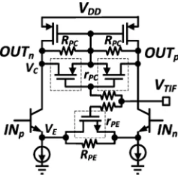
V-NPN BJTs are also used at the input stage of the IF am-plifier to eliminate the noise problem. Besides, the of a BJT transistor is much larger than that of a MOS transistor for the same bias current. Thus, the voltage gain of the VGA is im-proved using V-NPN BJTs. Conventionally, the quasi-exponen-tial function was realized by an - attenuation load with a com-bination of the constant resistance of the rigid resistance and the variable resistance implemented by a MOS transistor in the triode region, as shown in Fig. 11 [13], [14]. The impedance of the - attenuator can be expressed as , and has an approximate exponential characteristic in a certain region [13]. It is well known that is proportional to the gate overdrive voltage in the triode region. Thus, we can control the impedance of the attenuation load with the -exponential function. The - attenuation load is typically im-plemented at the load of the VGA. However, the output 1-dB compression point degrades in low-gain mode due to the limited input linear range, especially for a BJT input cell. Therefore, both loading and emitter - attenuators are ap-plied to maintain the of the VGA, especially in low-gain mode. The equivalent two-section - attenuation results in a wider linear-in-decibel tuning range 20 dB while typically a one-section - attenuator has a linear-in-decibel tuning re-gion of approximately 10 dB.
The schematic of the VGA with both loading/emitter -attenuators is shown in Fig. 11. A pMOS is employed at the drain node and an nMOS is chosen for the emitter degenera-tion. The drain–source resistance of the nMOS/ pMOS transistor in the triode region decreases/increases as the IF tuning voltage increases. Thus, the voltage gain has a positive gain slope with respect to the .
The differential voltage gain of the VGA can be easily for-mulated as
(19)
where and
while assuming , . is the rigid
resistor and is the nMOS/pMOS drain–source resistance in the triode region.
Fig. 12(a) shows the calculated numerator and the inverse of the denominator, , as a function
Fig. 12. (a) Numerator and inverse of the denominator of the voltage gain with different locations of transitions. (b) Corresponding as a function of .
of the IF tuning voltage . On the curve of , the transition occurs when becomes larger than
. The curve of has two transitions, and . transition occurs as becomes smaller than
, while occurs as becomes less than 1 (i.e., ). Typically, two tuning voltages should be used to control the two tuning operations. However, after proper design of bias points by transistor sizes, one tuning voltage can be adopted by properly overlapping the two constituent tuning curves. Since is the multiplication of both curves, different sequences of transitions result in different composite tuning curves. Fig. 12(b) shows the calculated for two sequences:
(1) and (2) ,
respectively. For the former sequence, there is a certain region with a constant voltage gain, which is not permissible for real applications, as shown in Fig. 12(b). On the contrary, a smooth tuning curve can be obtained by the latter sequence of
.
IV. MEASUREMENTRESULTS
A die photograph of the low-power low-noise tunable-band SH-DCR for U-NII bands is shown in Fig. 13, and the die size is 1.4 1.05 mm . On-wafer measurement facilitates the RF performance. The current consumption of the first/second-stage LNA is 2.5/0.8 mA, while the mixer and VGA consume 1
Fig. 13. Die photograph of the proposed SH-DCR with tunable narrowband LNA and wideband LO generator in a standard 0.18- m CMOS process.
Fig. 14. CG and NF with respect to RF frequency of the proposed SH-DCR.
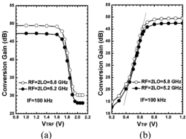
and 0.4 mA for each I/Q path, respectively. Besides, each LO buffer placed between 45 phase shifter and the PPF consumes 1.2 mA. Thus, the total current consumption is 8.5 mA at a 1.8-V supply. Fig. 14 shows the conversion gain (CG) and the NF as a function of RF frequency, while kHz. Due to the tunable RF band, two situations with maximum CG at 5.2/5.8 GHz are reported. The 5.2-GHz mode is tested for U-NII-1 band and U-NII-2 band, while the 5.8-GHz mode is tested for the U-NII-3 band. The peak CG at 5.2/5.8 GHz is 48/50 at its corresponding maximum condition, while the minimum NF is 4.5/4.8 dB. Fig. 15 shows the CG with
re-spect to the LO power when GHz
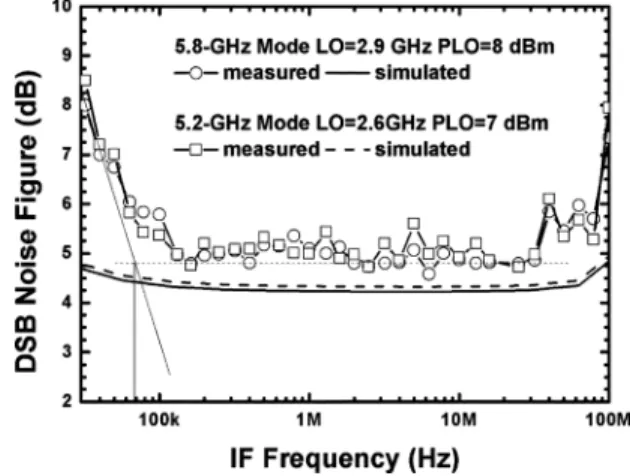
and GHz, respectively. 7/8-dBm LO power is applied for all the following measurements. Note that the effective LO voltage at the switching core is around 0.3 V by simulation. Fig. 16 shows the NF with respect to IF frequency when GHz, respectively, and the corner is around 70 kHz while the measured IF gain bandwidth is 50 MHz.
Fig. 17 shows the gain difference and I/Q phase error with respect to RF frequency. The phase/amplitude imbalance are extracted from the IF output waveforms measured by an os-cilloscope. The phase error has a bowl shape and is less than 1 within 4.5–6.4 GHz, while the amplitude imbalance is less
Fig. 15. CG with respect to LO power of the proposed SH-DCR.
Fig. 16. NF of the proposed SH-DCR.
than 0.6 dB. Fig. 18(a) shows the CG as a function of the
LNA RF tuning voltage at GHz,
re-spectively, while Fig. 18(b) indicates the CG with respect to the VGA IF tuning voltage . A tuning range exceeding 20 dB is achieved by each RF/IF tuning scheme. Fig. 19 shows the of the SH-DCR of ten samples. The minimum is 26/23 dBm at 5.2/5.8 GHz band, respectively. Note that using a differential LNA can further decrease the differential imbalance of the mixer inputs and thus increase the overall at the cost of extra dc current consumption.
The LO-to-RF isolation is over 75 dB, while the LO fre-quency ranging from 2.5 to 3.2 GHz, as shown in Fig. 20(a). As shown in Fig. 20(b), the dc offset due to self-mixing is strongly reduced because 63/70-dB LO rejection is obtained at
GHz, respectively. The worst case dc offset due to LO self-mixing can be calculated as [15]
(20) where represents the observed LO leakage at the RF port and stands for the CG of a mixer when the input signal is applied at LO frequency. Thus, the dc offset due to LO self-mixing is around 93 dBm (i.e., 5 V) at LO near both 2.6/2.9-GHz bands. In addition, the input return loss is greater than 10 dB covering 5–6 GHz, as shown in Fig. 21. Fi-nally, the circuit performance is summarized and compared with the state-of-the-art DCRs in Table I. A DCR with fundamental
Fig. 17. Gain difference and phase error of the IF I/Q outputs of the proposed SH-DCR.
Fig. 18. CG with respect to: (a) RF tuning voltage and (b) IF tuning voltage of the proposed SH-DCR.
Fig. 19. of the proposed SH-DCR.
mixers [16]–[18] has simpler downconversion circuit structures than that with SHMs [15], [19], [20], but has a worse output dc offset due to LO self-mixing. Both passive mixers [16], [17] and BJT active mixers (including using SiGe HBT technology [18]–[20] or V-NPN BJT in standard CMOS process in this study) have excellent noise corner when compared with the CMOS active mixers [15].
The proposed tunable-band LNA structure can save power consumption when compared to the wideband structure since the IF channel bandwidth is very narrow, as discussed in Section II. The BJT used as the IF stage also helps save
Fig. 20. (a) LO/2LO-to-RF isolation. (b) CG when and of the proposed SH-DCR.
Fig. 21. Input matching of the proposed SH-DCR.
current consumption because of its higher when compared with that of the nMOS device for the same dc current without degrading the noise property, as indicated in Section III-C. In addition, although the 45 phase shifter and the PPF are well-known building blocks, direct cascading two blocks for octet-phase generation may cause incredible loss due to the loading effect. After detailed analyses in Section III-B, the insertion of the inter-stage buffer amplifier not only keeps the phase accuracy of the phase shifter, but also solves the voltage
TABLE I
PERFORMANCECOMPARISONS OFSUB-HARMONICDIRECT-CONVERSIONRECEIVERS
loss of the PPF while the peaking inductors are placed after the PPF to further reduce the LO power loss. Through design optimizations above, the proposed tunable-band SH-DCR has less power consumption than these at similar bands in the references listed in Table I, but maintains excellent gain/noise performance.
V. CONCLUSION
A 0.18- m CMOS low-power SH-DCR has been demon-strated using a tunable narrowband RF LNA and wideband LO generator. A tunable narrowband structure has better perfor-mance than a wideband design at a given power consumption. In addition,V-NPNBJTshavebeenappliedtotheLOswitchingcore for noise improvement. With the resonance inductors and sub-harmonic mixing operation, the proposed downconversion mixer operates at three times the of the V-NPN BJTs. As a result, the demonstrated receiver achieves 48/50-dB voltage gain, 4.5/4.8-dB NF, and the noise corner is around 70 kHz when the RF band is tuned at 5.2/5.8 GHz, respectively. Besides, is 26/23 dBm, while the calculated dc offset is only around 5 V.
APPENDIXA
DERIVATION OF THEPEAKGAIN AND THECORRESPONDING
CRITERION OF THELC TANKWITHLOSSYINDUCTOR
As mentioned in Section II, the impedance of the LC tank with can be expressed as
(A1) Thus,
(A2) Take the differentiation by , occurs at
.
As a result,
(A3) Dividing (A2) by (A3), can be obtained as
(A4)
Further, substitute for simplicity and assume for a high- condition, can be rewritten as
The -dB bandwidth is calculated by letting . As a result,
(A7)
where . Thus,
(A8) , where and are the two solutions of (A8).
Besides, if and are the target bandwidth boundaries, the center frequency is because . The value for a target bandwidth from to can thus be obtained by
(A9)
APPENDIXB
DERIVATION OF THE TRANSIMPEDANCE GAIN OF ATRANSFORMER
The input impedance seen from the primary coil of the trans-former , shown in Fig. 5(a), can be expressed as
(B1)
The of the transformer can thus be calculated as follows:
(B2)
Here, and should be determined to find the at a certain operation frequency . For the equation above, is a constant at the target
frequency . occurs when , i.e.,
(B4)
where . Thus, can be rewritten as
(B5) where
and
To determine the optimal for , (or
) should be also achieved after complete calculation of
where is the sole “positive” solution. Thus, the optimal
turn ratio of a transformer by the
definition of .
Further, substituting into (B4) and (B5),
(B6) However, for a high-coupling condition
, and
. As a result, is not an applicable
so-lution and thus is typically chosen.
. Thus, the maximum can be rewritten as
(B7)
APPENDIXC
DERIVATION OF THETUNINGCAPABILITY OF ATRANSFORMER
WITHONLYONEVARACTOR INEITHERSIDE
A transformer with input/output capacitor loadings
is shown in Fig. 5(a). If only can be tuned, assume
and design ,
, where .
Since , (B4) can be rewritten as (C1)
where is nearly a constant
because is large. As a result,
(C2) and (C3) That is, (C4) REFERENCES
[1] L. Sheng, J. C. Jensen, and L. E. Larson, “A wide-bandwidth Si/SiGe HBT direct conversion sub-harmonic mixer/downconverter,” IEEE J.
Solid-State Circuits, vol. 35, no. 9, pp. 1329–1337, Sep. 2000.
[2] W. Kluge, F. Poegel, H. Roller, M. Lange, T. Ferchland, L. Dathe, and D. Eggert, “A fully integrated 2.4-GHz IEEE 802.15.4-compliant transceiver for ZigBee™ applications,” IEEE J. Solid-State Circuits, vol. 41, no. 12, pp. 2767–2775, Dec. 2006.
[3] I. Nam, K. Choi, J. Lee, H.-K. Cha, B.-I. Seo, K. Kwon, and K. Lee, “A 2.4 GHz low-power low-IF receiver and direct-conversion trans-mitter in 0.18- m CMOS for IEEE 802.15.4 WPAN applications,”
IEEE Trans. Microw. Theory Tech., vol. 55, no. 4, pp. 682–689, Apr.
2007.
[4] M. Brandolini, P. Rossi, D. Sanzogni, and F. Svelto, “ dBm CMOS direct downconversion mixer for fully integrated UMTS re-ceivers,” IEEE J. Solid-State Circuits, vol. 41, no. 3, pp. 552–559, Mar. 2006.
[5] M. Zargari, M. Terrovitis, S. H.-M. Jen, B. J. Kaczynski, M. Lee, M. P. Mack, S. S. Mehta, S. Mendis, K. Onodera, H. Samavati, W. W. Si, K. Singh, A. Tabatabaei, D. Weber, D. K. Su, and B. A. Wooley, “A single-chip dual-band tri-mode CMOS transceiver for IEEE 802. 11a/b/g wireless LAN,” IEEE J. Solid-State Circuits, vol. 39, no. 12, pp. 2239–2249, Dec. 2004.
[6] M. Goldfarb, E. Balboni, and J. Cavey, “Even harmonic double-bal-anced active mixer for use in direct conversion receivers,” IEEE J.
Solid-State Circuits, vol. 38, no. 10, pp. 1762–1766, Oct. 2003.
[7] K.-J. Koh, M.-Y. Park, C.-S. Kim, and H.-K. Yu, “Subharmonically pumped CMOS frequency conversion (up and down) circuits for 2-GHz WCDMA direct-conversion transceiver,” IEEE J. Solid-State
Circuits, vol. 39, no. 6, pp. 871–884, Jun. 2004.
[8] D. Manstretta, M. Brandolini, and F. Svelto, “Second-order inter-mod-ulation mechanisms in CMOS downconverters,” IEEE J. Solid-State
Circuits, vol. 38, no. 3, pp. 394–406, Mar. 2003.
[9] W.-Z. Chen and W.-H. Chen, “Symmetric 3-D passive components for RF ICs application,” in IEEE MTT-S Int. Microw. Symp. Dig., Jun. 2003, pp. 599–602.
[10] R. S. Carson, Radio Communications Concepts: Analog. New York: Wiley, 1990.
[11] J.-S. Syu, C. C. Meng, Y.-H. Teng, and H.-Y. Liao, “Large improve-ment in image rejection of double-quadrature dual-conversion low-IF architectures,” IEEE Trans. Microw. Theory Tech., vol. 58, no. 7, pp. 1703–1712, Jul. 2010.
[12] B. G. Perumana, R. Mukhopadhyay, S. Chakraborty, C.-H. Lee, and J. Laskar, “A low-power fully monolithic subthreshold CMOS receiver with integrated LO generation for 2.4 GHz wireless PAN applications,”
IEEE J. Solid-State Circuits, vol. 43, no. 10, pp. 2229–2238, Oct. 2008.
[13] Y.-S. Youn, J.-H. Choi, M.-H. Cho, S.-H. Han, and M.-Y. Park, “A CMOS IF transceiver with 90 dB linear control VGA for IMT-2000 ap-plication,” in VLSI Circuits Tech. Symp. Dig., Jun. 2003, pp. 131–134. [14] Y.-S. Youn, C.-S. Kim, N.-S. Kim, and H.-K. Yu, “A 1 GHz-band low distortion up-converter with a linear in dB control VGA for digital TV tuner,” in IEEE Radio Freq. Integr. Circuits Symp. Dig., May 2001, pp. 257–260.
[15] H.-C. Chen, T. Wang, and S.-S. Lu, “A 5–6 GHz 1-V CMOS direct-conversion receiver with an integrated quadrature coupler,” IEEE J.
Solid-State Circuits, vol. 42, no. 9, pp. 1963–1975, Sep. 2007.
[16] S. Zhou and M.-C. F. Chang, “A CMOS passive mixer with low flicker noise for low-power direct-conversion receiver,” IEEE J. Solid-State
Circuits, vol. 40, no. 5, pp. 1084–1093, May 2005.
[17] M. Valla, G. Montagna, R. Castello, R. Tonietto, and I. Bietti, “A 72-mW CMOS 802.11a direct conversion front-end with 3.5-dB NF and 200-kHz noise corner,” IEEE J. Solid-State Circuits, vol. 40, no. 4, pp. 970–977, Apr. 2005.
[18] S. Chakraborty, S. K. Reynolds, H. Ainspan, and J. Laskar, “Develop-ment of 5.8GHz SiGe BiCMOS direct conversion receivers,” in IEEE
MTT-S Int. Microw. Symp. Dig., Jun. 2003, pp. 1551–1553.
[19] B. G. Choi and C. S. Park, “A 5.8 GHz SiGe HBT direct-conversion I/Q-channel sub-harmonic mixer for low power and simplified receiver architecture,” in IEEE MTT-S Int. Microw. Symp. Dig., Jun. 2005, pp. 177–180.
[20] R. Svitek and S. Raman, “5–6 GHz SiGe active I/Q subharmonic mixers with power supply noise effect characterization,” IEEE
Mi-crow. Wireless Compon. Lett., vol. 14, no. 7, pp. 319–321, Jul. 2004.
Jin-Siang Syu (S’09) was born in Taoyuan, Taiwan,
in 1984. He received the B.S. degree in communi-cation engineering from National Chiao Tung Uni-versity, Hsinchu, Taiwan, in 2006, and is currently working toward the Ph.D. degree in electrical engi-neering at National Chiao Tung University.
His current research interests are in the areas of RF integrated circuits (RFICs).
Mr. Syu is a member of Phi Tau Phi.
Chinchun Meng (M’02) received the B.S. degree in
electrical engineering from National Taiwan Univer-sity, Taipei, Taiwan, in 1985, and the Ph.D. degree in electrical engineering from the University of Cal-ifornia, Los Angeles (UCLA), in 1992.
He is currently a Full Professor with the Depart-ment of Electrical Engineering, National Chiao Tung University, Hsinchu, Taiwan. His current research in-terests are in the areas of RFICs, microwave and mil-limeter-wave integrated circuits (ICs).