IEEE ELECTRON DEVICE LETTERS, VOL. 29, NO. 10, OCTOBER 2008 1105
Improvement of the Performance of TiHfO MIM
Capacitors by Using a Dual Plasma
Treatment of the Lower Electrode
C. H. Cheng, H. C. Pan, C. C. Huang, C. P. Chou, C. N. Hsiao, J. Hu, M. Hwang, T. Arikado,
S. P. McAlister, Senior Member, IEEE, and Albert Chin, Senior Member, IEEE
Abstract—We show that a conventional nitrogen plasma
treat-ment is insufficient to suppress the formation of an interfacial layer at the bottom electrode of TiHfO metal–insulator–metal (MIM) capacitors. However, the capacitance density and leakage current of TaN/TiHfO/TaN MIM capacitors monotonically im-prove by exposing the lower TaN electrode to an additional oxy-gen plasma treatment. By performing dual oxyoxy-gen and nitrooxy-gen plasma treatments on the lower electrode, the leakage current was 4.8× 10⁻⁶A/cm2(at−1 V) at a 28 fF/μm2capacitance density. Index Terms—High κ, metal–insulator–metal (MIM), plasma
treatment, TiHfO.
I. INTRODUCTION
T
HE TECHNOLOGY roadmap for metal–insulator–metal (MIM) capacitors [1]–[16], which are used for analog, RF, and DRAM functions in integrated circuits, specifies a continuing increase of the capacitance density ε0κ/tκ andlower leakage currents. To achieve this goal, higher κ TiO-based dielectrics—such as TiTaO, TiLaO, TiHfO [11]–[13], and SrTiO3(STO) [14]–[16]—are needed for the MIM devices.
Unfortunately, there is an interfacial reaction during device processing at the lower high-κ dielectric/metal interface [14]. This reduces the capacitance density and increases the leakage current, and this reaction increases in importance as the capaci-tance equivalent thickness decreases to 1 nm. To inhibit the re-action, a nitrogen plasma treatment can be applied to the TaN or TiN bottom electrodes [14]–[16]. Here, we report an improved surface treatment for TaN electrodes. Following a conventional nitrogen plasma treatment, exposing the bottom TaN to oxygen plasma monotonically increased the capacitance density from
Manuscript received March 5, 2008; revised May 22, 2008. Current version published September 24, 2008. The work at the National Chiao Tung University was supported by Tokyo Electron Ltd. The review of this letter was arranged by Editor A. Z. Wang.
C. H. Cheng and C. P. Chou are with the Department of Mechanical Engineering, National Chiao Tung University, Hsinchu 300, Taiwan, R.O.C.
H. C. Pan and C. N. Hsiao are with the Instrument Technology Research Center, National Applied Research Laboratories, Hsinchu 300, Taiwan, R.O.C. C. C. Huang is with the Department of Electronics Engineering, National Chiao Tung University, Hsinchu 300, Taiwan, R.O.C.
J. Hu, M. Hwang, and T. Arikado are with Tokyo Electron Ltd., Tokyo 107-8481, Japan.
S. P. McAlister is with the National Research Council of Canada, Ottawa, ON K1A 0R6, Canada.
A. Chin is with the Department of Electronics Engineering, National Chiao Tung University, Hsinchu 300, Taiwan, R.O.C., and also with the Nano-Electronics Consortium of Taiwan, Hsinchu 300, Taiwan, R.O.C. (e-mail: [email protected]).
Digital Object Identifier 10.1109/LED.2008.2000945
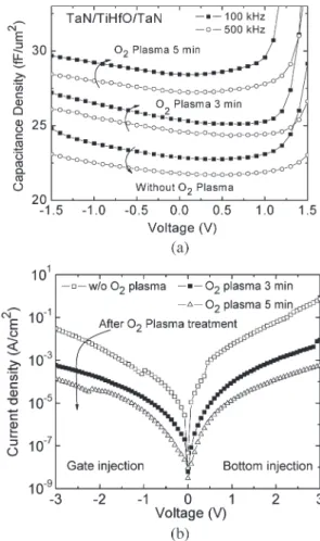
Fig. 1. (a) C–V and (b) J –V characteristics for TaN/TiHfO/TaN MIM capacitors measured after the indicated plasma treatments.
22 to 28 fF/μm2. This combined oxygen and nitrogen plasma
treatment also improved the leakage current by two orders of magnitude. Such an improvement occurs because the interfacial reaction is reduced during device processing. This was seen in cross-sectional transmission electron microscopy (TEM). We measured a leakage current of 4.8× 10⁻⁶ A/cm2 in our
28-fF/μm2 density TaN/TiHfO/TaN MIM capacitors. These
data compare well with other high-κ MIM capacitors [1]– [16], even when higher workfunction Ir [11]–[15] or Ni [16] electrodes are used.
II. EXPERIMENTALPROCEDURE
The high-κ TiHfO MIM capacitors were fabricated on stan-dard Si wafers. For VLSI backend integration, a 2-μm-thick
1106 IEEE ELECTRON DEVICE LETTERS, VOL. 29, NO. 10, OCTOBER 2008
TABLE I
COMPARISON OFMIM CAPACITORSHAVINGVARIOUSDIELECTRICS ANDMETALELECTRODES
SiO2isolation layer was deposited on the Si substrates. Then, a
TaN/Ta (50 nm/200 nm) bilayer was deposited and used as the bottom capacitor electrode. The nitrogen plasma was applied to the TaN surface [13]–[15]. This was followed by an O2plasma
treatment to increase the oxidation resistance before the high-κ dielectric deposition and postdeposition annealing (PDA). An
∼12-nm-thick TixHf1−xO (x∼ 0.67) film was deposited by
RF sputtering HfO2 and TiO2 targets in a gas mixture of
O2 (1 sccm) and Ar (10 sccm), followed by a 400 ◦C PDA
in an oxygen ambient, to reduce the defects and the leakage current [3]. Finally, a 50-nm layer of TaN was deposited and patterned to form the top electrode. The TiHfO thickness and the interfacial layer between TiHfO and bottom TaN were measured by cross-sectional TEM. A large capacitor size of 150 μm× 150 μm was used to ensure that any dimensional variations were unimportant. The fabricated MIM devices were characterized by C–V and J –V measurements.
III. RESULTS ANDDISCUSSION
In Fig. 1(a) and (b), we show the C–V and J –V character-istics of TiHfO capacitors with and without the second oxygen plasma treatment. The capacitance density increased from 22 to 28 fF/μm2, as the lower TaN electrode was exposed to oxygen plasma for longer times. Correspondingly, the leakage current at−1 V decreased from 2.5 × 10⁻⁴to 4.8× 10⁻⁶A/cm2with increasing oxygen exposure. Therefore, the increasing exposure time to oxygen plasma improves both the capacitance density and the leakage current. The comparison of our data with those for other MIM capacitors appears in Table I. The performance of our TaN/TiHfO/TaN capacitors is comparable with the best reported MIM devices, such as Ir/TiTaO/TaN (23 fF/μm2
den-sity) [11], [12] or Ni/STO/TaN (25-fF/μm2density) capacitors
[16], which used higher workfunction Ir (5.3 eV) and Ni (5.1 eV) top electrodes than this TaN (∼4.6 eV) case. The high workfunction electrode is particularly important for the leakage current at a low voltage due to the Schottky emission mechanism [15], [17]. Our result indicates the importance of an additional oxygen plasma treatment on the lower electrode.
We have also measured the variation of the capacitance (ΔC/C) as a function of voltage. In Fig. 2, we show such (ΔC/C)−V data. The voltage dependence of ΔC/C is ex-pressed as βV + αV2 [8]–[12], where β and α are the linear
Fig. 2. (ΔC/C)−V characteristics for TaN/TiHfO/TaN MIM capacitors following various plasma treatments.
and quadratic coefficients of (ΔC/C)−V , respectively. Here,
α is the important factor for capacitors since the effects of β
can be compensated in the circuit design [8]. Increasing the exposure time of the bottom TaN to oxygen plasma decreased
α from 17 858 to 3851 ppm/V2. Since α rapidly improves with decreasing capacitance density [14], further α reduction is possible at the lower capacitance density used for analog/RF applications.
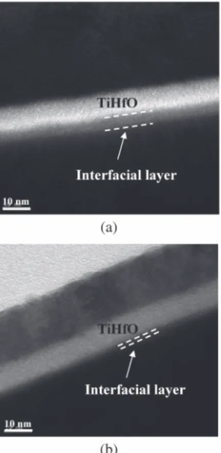
To understand these performance improvements, we exam-ined the devices using cross-sectional TEM. In Fig. 3(a) and (b), we compare the TEM images for the TiHfO structure without and with the oxygen plasma treatment. A clear in-terfacial region, which is ∼3-nm wide, can be seen in the conventional nitrogen-only plasma-treated TaN, giving a total thickness of ∼15 nm. In contrast, the combined oxygen and nitrogen plasma-treated TaN showed reduced interfacial reac-tions. A thickness of ∼12 nm was measured for the TiHfO dielectric—indicating a κ value of 38—at a capacitance density of 28 fF/μm2. The possible reason for the large improvement
given by the oxygen plasma treatment may be the larger bond enthalpy of TaO (799 kJ/mol) compared with that of TaN (611 kJ/mol) [18]. When applying only a nitrogen plasma treatment, the lower TaN will be oxidized to TaON during un-avoidable PDA, due to the thermodynamically favorable larger bond enthalpy—this would lower the capacitance density. The significantly smaller interfacial layer with the oxygen plasma
CHENG et al.: IMPROVEMENT OF THE PERFORMANCE OF TiHfO MIM CAPACITORS 1107
Fig. 3. Cross-sectional TEM images of the TiHfO structure (a) with only a nitrogen plasma treatment and (b) with both a nitrogen and a second oxygen plasma treatment.
treatment may be due to the formation of high-quality TaON by highly reactive oxygen plasma, which further decreases oxygen diffusion into underneath TaN to form poor-quality thermal TaON at a low temperature during PDA.
IV. CONCLUSION
We have shown that a nitrogen plasma treatment alone cannot suppress the interfacial layer formation that causes the degraded capacitance density and leakage current in TaN/TiHfO/TaN MIM capacitors. By using an additional oxygen plasma treat-ment, the interfacial reactions and growth were reduced, leading to a higher capacitance density and a lower leakage current.
REFERENCES
[1] C.-M. Hung, Y.-C. Ho, and I.-C. Wu, “High-Q capacitors implemented in a CMOS process for low-power wireless applications,” in Proc. IEEE MTT-S Int. Microw. Symp. Dig., 1998, pp. 505–511.
[2] J. A. Babcock, S. G. Balster, A. Pinto, C. Dirnecker, P. Steinmann, R. Jumpertz, and B. El-Kareh, “Analog characteristics of metal–insulator– metal capacitors using PECVD nitride dielectrics,” IEEE Electron Device Lett., vol. 22, no. 5, pp. 230–232, May 2001.
[3] C. H. Ng, K. W. Chew, and S. F. Chu, “Characterization and compari-son of PECVD silicon nitride and silicon oxynitride dielectric for MIM capacitors,” IEEE Electron Device Lett., vol. 24, no. 8, pp. 506–508, Aug. 2003.
[4] T. Ishikawa, D. Kodama, Y. Matsui, M. Hiratani, T. Furusawa, and D. Hisamoto, “High-capacitance Cu/Ta2O5/Cu MIM structure for SoC
applications featuring a single-mask add-on process,” in IEDM Tech. Dig., 2002, pp. 940–942.
[5] S. B. Chen, J. H. Lai, A. Chin, J. C. Hsieh, and J. Liu, “High density MIM capacitors using Al2O3and AlTiOxdielectrics,” IEEE Electron Device
Lett., vol. 23, no. 4, pp. 185–187, Apr. 2002.
[6] S. B. Chen, J. H. Lai, K. T. Chan, A. Chin, J. C. Hsieh, and J. Liu, “Frequency-dependent capacitance reduction in high-k AlTiOx
and Al2O3gate dielectrics from IF to RF frequency range,” IEEE
Elec-tron Device Lett., vol. 23, no. 4, pp. 203–205, Apr. 2002.
[7] X. Yu, C. Zhu, H. Hu, A. Chin, M. F. Li, B. J. Cho, D.-L. Kwong, P. D. Foo, and M. B. Yu, “A high-density MIM capacitor (13 fF/μm2) using ALD HfO2dielectrics,” IEEE Electron Device Lett., vol. 24, no. 2,
pp. 63–65, Feb. 2003.
[8] H. Hu, S. J. Ding, H. F. Lim, C. Zhu, M. F. Li, S. J. Kim, X. F. Yu, J. H. Chen, Y. F. Yong, B. J. Cho, D. S. H. Chan, S. C. Rustagi, M. B. Yu, C. H. Tung, A. Du, D. My, P. D. Fu, A. Chin, and D. L. Kwong, “High performance HfO2−Al2O3 laminate MIM capacitors by ALD
for RF and mixed signal IC applications,” in IEDM Tech. Dig., 2003, pp. 379–382.
[9] S. J. Kim, B. J. Cho, M.-F. Li, C. Zhu, A. Chin, and D. L. Kwong, “HfO2 and lanthanide-doped HfO2 MIM capacitors for RF/mixed IC
applications,” in VLSI Symp. Tech. Dig., 2003, pp. 77–78.
[10] S. J. Kim, B. J. Cho, M. B. Yu, M.-F. Li, Y.-Z. Xiong, C. Zhu, A. Chin, and D. L. Kwong, “High capacitance density (> 17 fF/μm2) Nb
2O5-based
MIM capacitors for future RF IC applications,” in VLSI Symp. Tech. Dig., 2005, pp. 56–57.
[11] K. C. Chiang, A. Chin, C. H. Lai, W. J. Chen, C. F. Cheng, B. F. Hung, and C. C. Liao, “Very high-κ and high density TiTaO MIM capacitors for analog and RF applications,” in VLSI Symp. Tech. Dig., 2005, pp. 62–63.
[12] K. C. Chiang, C. H. Lai, A. Chin, T. J. Wang, H. F. Chiu, J. R. Chen, S. P. McAlister, and C. C. Chi, “Very high density (23 fF/μm2) RF MIM
capacitors using high-κ TiTaO as the dielectric,” IEEE Electron Device Lett., vol. 26, no. 10, pp. 728–730, Oct. 2005.
[13] C. H. Cheng, H. C. Pan, H. J. Yang, C. N. Hsiao, C. P. Chou, S. P. McAlister, and A. Chin, “Improved high-temperature leakage in high-density MIM capacitors by using a TiLaO dielectric and an Ir electrode,” IEEE Electron Device Lett., vol. 28, no. 12, pp. 1095–1097, Dec. 2007.
[14] K. C. Chiang, C. C. Huang, A. Chin, W. J. Chen, H. L. Kao, M. Hong, and J. Kwo, “High performance micro-crystallized TaN/SrTiO3/TaN
capacitors for analog and RF applications,” in VLSI Symp. Tech. Dig., 2006, pp. 126–127.
[15] K. C. Chiang, C. C. Huang, A. Chin, G. L. Chen, W. J. Chen, Y. H. Wu, and S. P. McAlister, “High performance SrTiO3 metal–insulator–metal
capacitors for analog applications,” IEEE Trans. Electron Devices, vol. 53, no. 9, pp. 2312–2319, Sep. 2006.
[16] K. C. Chiang, C. H. Cheng, H. C. Pan, C. N. Hsiao, C. P. Chou, A. Chin, and H. L. Hwang, “High-temperature leakage improvement in metal–insulator–metal capacitors by work-function tuning,” IEEE Electron Device Lett., vol. 28, no. 3, pp. 235–237, Mar. 2007.
[17] H. J. Yang, A. Chin, W. J. Chen, C. F. Cheng, W. L. Huang, I. J. Hsieh, and S. P. McAlister, “A program-erasable high-κ Hf0.3N0.2O0.5MIS
ca-pacitor with good retention,” IEEE Electron Device Lett., vol. 28, no. 10, pp. 913–915, Oct. 2007.
[18] D. S. Yu, A. Chin, C. H. Wu, M.-F. Li, C. Zhu, S. J. Wang, W. J. Yoo, B. F. Hung, and S. P. McAlister, “Lanthanide and Ir-based dual metal-gate/HfAlON CMOS with large work-function difference,” in IEDM Tech. Dig., 2005, pp. 649–652.