國立交通大學
顯示科技研究所
碩士論文
高穿透效率之
立體顯示器液晶畫素設計
High Transmittance LC Pixel Design for
Multi-View 3D Mobile Display
研究生:吳其霖
指導教授:謝漢萍 教授
黃乙白 助理教授
高穿透效率之
立體顯示器液晶畫素設計
High Transmittance LC Pixel Design for
Multi-View 3D Mobile Display
研究生:吳其霖 Student : Chi-Lin Wu
指導教授:謝漢萍、黃乙白
Advisor : Dr. Han-Ping D. Shieh and Dr. Yi-Pai Huang
國立交通大學 電機學院
顯示科技研究所
碩士論文
A Thesis
Submitted to Display Institute
College of Electrical Engineering and Computer Engineering
National Chiao Tung University
in Partial Fulfillment of the Requirements
for the Degree of Master
in
Display Institute
July 2008
Hsinchu, Taiwan
Republic of China
中華民國 九十七 年 七 月
i
高穿透效率之
立體顯示器液晶畫素設計
碩士研究生:吳其霖 指導教授:謝漢萍教授
黃乙白助理教授
國立交通大學 顯示科技研究所
摘 要
為了得到更自然的立體影像,近年來已吸引許多專家及廠商投入立體顯示器 的發展。傳統立體顯示器中液晶面板未考慮立體顯示之應用,在配合視差遮罩製 作成立體顯示器時,其光使用效率與立體影像品質均因面板畫素特性與參數未能 配合。因此,立體液晶顯示系統仍面臨了許多的問題,諸如影像解析度不夠高、 亮度不夠亮、每個視點的影像亮度不均等。若影像解析度提升上,則影像亮度會 下降更多。因此,首要改善的問題是亮度,本論文針對亮度低等問題提出配合自 立體顯示器之液晶畫素與面板設計的方法。主要為各畫素具有不同之視角特性, 以及各畫素非有效區域或不透光部份置於不同之畫素相對位置。以配合視差遮罩 之佈局,進而提升立體顯示之影像品質與效率。 模擬中,考慮各液晶畫素具有不同之視角特性,及各畫素非有效區域或不透 光部份依視差遮罩置於適當的區域來提升影像亮度。因此,與傳統視差遮罩立體 顯示器相比,亮度可提升近一倍。實驗上,各液晶畫素依然具有相同之視角特性, 但畫素非有效區域或不透光部份依視差遮罩置於適當的區域來提升亮度,亮度上 升了約 60%.ii
High Transmittance LC Pixel Design for
Multi-View 3D Mobile Display
Student: Chi-Lin Wu Advisor: Dr. Han-Ping D. Shieh
Dr. Yi-Pai Huang
Display Institute
National Chiao Tung University
Abstract
In order to get more natural 3D sensation from displays, many researchers and manufacturers were attracted to invest in the development of 3D display technology in recent years. In conventional autostereoscopic 3D displays, due to the fact that the pixel designs of the liquid crystal displays were not optimized for 3D displays, the issues of lower brightness and degraded images quality were produced. The major issue is lower brightness with unbalanced brightness between viewing zones. In order to increase image brightness and minimize unbalanced brightness issue, we proposed a pixel layout where blocking light components, such as storage capacitor, was optimized for the parallax barrier to increase the transparent area. Beside, in order to balance the brightness between viewing zones, each pixel has its own transmittance curve which is optimized for specific viewing zone.
In the simulation results, the brightness of a parallax barrier 3D display with proposed pixel layout is increased by a factor of 2 compared to that of 3D display based on conventional pixel layout. A 2.83” 6-view 3D mobile display has been demonstrated. The pixel layout with slanted storage capacitor is fabricated, but each pixel still has the same transmittance curve. From the experimental results, the brightness is increased by a factor of 1.6.
iii
誌 謝
首先誠摯的感謝指導老師謝漢萍老師及黃乙白老師對於研究態度及英文能 力的教導,以及提供豐富的資源與完善研究環境,使我得以在碩士生涯提升了專 業及英文的能力,順利完成此論文。此外,也感謝口試委員鄭惟中、陳政寰助理 教授及陳伯綸博士所提供的寶貴意見,使本論文更加的完善。 在此特別感謝友達光電許時嘉學長對於研究與專業知識的指導與協助及生 活上的照顧,在忙碌的工作期間,耐心幫助我解決問題,受益良多。另外,在友 達也常受林祥麟學長照顧,讓我不會餓肚子。此外我要感謝友達光電諸位合作同 仁提供我寶貴的意見及實作的協助,讓整個研究進展的更順利。除此之外,我要 感謝一起合作的清大動機所莊尚智同學,給予我最深入的討論,讓研究可以順利 進行。 在實驗室的日子裡,感謝有鄭榮安、林芳正、楊柏儒、方仁宇、陳均合、莊 喬舜、李企桓、鄭裕國、許精益、陳國宗等學長們提供各方面的指導與協助,也 感謝坤岳、侑興、雅婷、勇智、振宇、韻竹、友群等學長姊們讓我的生活更加精 彩。同時感謝勝昌、凌嶢、建良、國振、仁杰、景明、明農、宛徵等同學們在課 業、研究、生活上的幫助與分享,並伴我一起度過兩年碩士班的日子。我也感謝 實驗室的學弟妹們與助理小姐,感謝你/妳們的幫忙及讓實驗室充滿歡愉的氣氛。 最後,我要感謝我的爸媽、哥哥、妹妹及關心我的家人和朋友們,感謝爸媽 多年來的支持,使我能無後顧之憂的研究與學習,給我一個這麼好的學習環境, 並順利完成碩士學業。在此,我將這份喜悅與每位關心我的人分享。iv
Table of Contents
Abstract (Chinese) ... i
Abstract (English) ... ii
Acknowledgments ... iii
Table of Contents ...iv
Figure Captions ...vi
List of Tables...ix
Chapter 1 Introduction...1
1.1 Preface...1
1.2 Principle of 3D vision ...2
1.3 Introduction to 3D displays technology...4
1.3.1 Stereoscopic displays ...4
1.3.2 Non-glasses displays...4
1.3.3 Multiplexed displays...5
1.4 Motivation and objective of this thesis ...10
1.5 Organization of this thesis...11
Chapter 2 Principles of LCDs with Optical Films...12
2.1 Optical properties of VA cells ...12
2.2 Phase retardation at oblique incidence...14
2.3 Conventional MVA-b LCDs ...17
2.3.1 Pixel ...17
2.3.2 Optical films ...18
2.4 Summary ...19
Chapter 3 Pixel Design and Simulation for High Transmittance of
3D Displays ...20
3.1 Issues of conventional 3D displays...20
3.2 Parameters affecting brightness of 3D displays...22
v
3.3.1 Changing the thickness of negative c plate VA...25
3.3.2 Normally White Single Domain VA ...28
3.4 Pixel array design...31
3.4.1 Bumpless...31
3.4.2 Slanted storage capacitor ...32
3.5 Aperture ratio of parallax barrier ...34
3.6 Discussion ...35
3.7 Summary ...36
Chapter 4 Fabrication Technologies and Measurement Instruments
...38
4.1 Fabrication process ...38
4.2 Measurement instruments ...42
Chapter 5 Measurement Results and Discussion...44
5.1 Introduction...44
5.2 Measurement results and discussion...44
5.2.1 Brightness ...46
5.2.2 Crosstalk ...47
5.3 Summary ...48
Chapter 6 Conclusions and Future Work...50
6.1 Conclusions...50
6.2 Future work...51
vi
Figure Captions
Fig. 1-1 History of the display technology...1
Fig. 1-2 Depth cues...2
Fig. 1-3 Binocular parallax. ...3
Fig. 1-4 Principles of the spatial and time-multiplexed autostereoscopic 3D displays. 5 Fig. 1-5 3D display based on sequentially switching backlight with focusing foil. ...6
Fig. 1-6 Spatial multiplexed displays: (a) parallax barrier and (b) lenticular lenses. ....7
Fig. 1-7 Principle of multi-view 3D displays...8
Fig. 1-8 The slanted arrangement of the lenticular lens and pixels in the Philips multi-view display...9
Fig. 2-1 Schematic drawing showing the orientation of the polarizer axes, LC directors of a general VA-LCD in the xy plane...13
Fig. 2-2 Phase retardation at oblique incidence. ...15
Fig. 2-3 Phase retardation of a plate at oblique incidence...16
Fig. 2-4 (a) MVA-b pixel layout and (b) cross-section of the MVA-b pixel...17
Fig. 2-5 The optical configuration of conventional MVA-b mode. ...18
Fig. 2-6 Phase retardation with negative c plates. ...19
Fig. 3-1 6-view slanted parallax barrier 3D display...21
Fig. 3-2 Schematic drawing of a 6 views parallax barrier display...21
Fig. 3-3 Transmittance of (a) conventional LC and (b) proposed LC. ...22
Fig. 3-4 The configuration of the parallax barrier 3D display. ...23
Fig. 3-5 Viewing angle of (a) conventional displays, (b) conventional 3D displays, and (c) single domain displays. ...24
Fig. 3-6 The difference in brightness between multi-domain VA and single domain VA ...24
vii
Fig. 3-8 The optical configuration of single-domain VA...25
Fig. 3-9 Maximum transmittance can be generated at a specific viewing angle by changing the thickness of the negative c plate...26
Fig. 3-10 Transmittance profiles of single-domain VA and conventional MVA-b for different kinds of pixels. ...27
Fig. 3-11 The optical configuration of Normally White Single Domain VA...28
Fig. 3-12 The LC alignment directions for various pixels...28
Fig. 3-13 Transmittance profiles of Normally White Single Domain VA and conventional MVA-b for different kinds of pixels...29
Fig. 3-14 The transmittance comparison of Normally White Single Domain VA and conventional MVA-b for each view. ...30
Fig. 3-15 A parallax barrier 3D display with conventional MVA-b pixel design. ...31
Fig. 3-16 The 6th pixel layout of (a)conventional 2.83” MVA-b mode (b) NW single domain VA with azimuth angle of ITO fine slit 110°. ...32
Fig. 3-17 A parallax barrier using proposed pixel with slanted storage capacitor. ...33
Fig. 3-18 The viewing zone 3 of 3D displays using conventional and proposed pixels. ...33
Fig. 3-19 The modified pixel layout. ...34
Fig. 3-20 Conventional and modified pixel layouts...34
Fig. 3-21 Illustration of 2D/3D switchable display with the same resolution. ...35
Fig. 3-22 Pixel layout for fabrication...36
Fig. 4-1 TFT LCD fabrication process flow. ...38
Fig. 4-2 Fabrication steps for top-gate poly-si TFTs[25]. ...40
Fig. 4-3 Fabrication process of polymer layer[22]...42
Fig. 4-4 Conoscope. ...43
Fig. 4-5 The principle diagram of Conoscope. ...43
viii
Fig. 5-2 Test patterns used to measure the crosstalk of each viewing zone...47 Fig. 5-3 The illustration of measurement of inputting the test pattern (BBWBBB)....48 Fig. 6-1 Slanted pixel layout...51
ix
List of Tables
Table 3-1 The improvement of each factor. ...37 Table 5-1 Specifications of the parallax barrier and 2.83” LCDs...45 Table 5-2 Brightness increase ratio of the proposed pixel layout compared to 3D display with conventional MVA-b pixel layout...46 Table 5-3 Crosstalk was measured by Conoscope...48 Table 5-4 Comparisons of 3D displays with conventional and proposed pixel layouts. ...49
1
Chapter 1
Introduction
1.1 Preface
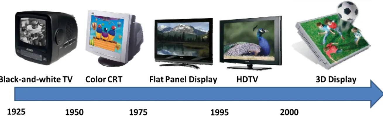
For the display technology industry, there have been several milestones in past 120 years as shown in Fig. 1-1[1]. K. F. Braun invented the cathode ray tube (CRT) in 1897. Human eyes have three different kinds of cone cells, thus humans can sense color. Thus we had the displays technological progress from black and white to colorful cathode ray tube (CRTs). After that, Flat panel displays became widely used because CRTs are bulky. In order to get higher image quality, many researchers have focused on high- definition televisions (HDTVs). However, the image qualities are still not as good as the real world vision perceived by humans in the real world. There is no stereoscopic sensation in the above technologies which are thus classified as 2D displays.
Black‐and‐white TV Color CRT Flat Panel Display HDTV 3D Display
1925 1950 1975 1995 2000
2
Human eyes have many kinds of complex mechanisms to perceive depth. In order to get more natural 3D sensation from displays, 3D display technology is expected to be the dominant next generation display technology.
1.2 Principle of 3D vision
Three dimensional information results from visual system and brain cognitive system. In the real world, more than one depth cue is available to us simultaneously. Depth cues can be divided into three kinds of cues: monocular, binocular, and oculomotor cues, as shown in Fig. 1-2[2].
Fig. 1-2 Depth cues.
Convergence
Oculomotor cue based on the inward focus of the eyes with a close object. Convergence is ineffective at long distances (~20m).
Accommodation
Accommodation is adjustment in the shape of the lens of the eye when focusing on objects. Accommodation is effective at short distances (~3m).
3
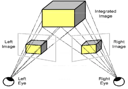
Binocular Parallax
Binocular parallax is based on the disparity in the retinal image of the two eyes. The average distance between the pupils of the human eyes is approximately 65 mm. Binocular depth cues are those cues which arise from using two separated eyes to view the world (Fig. 1-3). Our brain can fuse these disparate images to produce strong perceptions of depth as well as an object form. Binocular parallax causes the phenomenon of stereopsis (Levine and Shefner, 1991).
Fig. 1-3 Binocular parallax.
Motion Parallax
Motion Parallax is the case when either an object in the scene or the observer's head moves. Depth cues are often provided by movement of the observer or of objects in the visual environment.
Others
The other monocular depth cues are learned or based on experience and over time observers learn the physical significance of different retinal images and their relation to
4
objects in the real world. These include interposition, linear perspective etc.
In the real world, human can easily perceive the depth information by using the above-mentioned depth cues. In displaying visual 3D information, due to the fact that displays can not produce 3D information by the occulomotor cues (convergence and accommodation), 3D displays, in general have to utilize binocular and motion parallax to produce 3D images.
1.3 Introduction to 3D displays technology
3D Displays can be divided into stereoscopic and non-glasses displays. For different applications e.g. entertainment, business, personal, public etc there are many kinds of 3D displays that are suitable for each category.
1.3.1 Stereoscopic displays
For stereoscopic displays, users are required to wear devices, such as polarized glasses, which ensure the left and right eye’s images are seen by the correct eye. Many stereoscopic displays have been proposed[3]. Most of them have been widely used in many fields, such as cinema for multiple observer applications, but suffer from the fact that viewers have to wear devices.
1.3.2 Non-glasses displays
Non-glasses displays are 3D displays that do not require users to wear any device to separate the left and right images for each eye. Various kinds of Non-glasses technologies, such as volumetric type[4], holographic type[5], integral imaging type[6], and 2D multiplexed type (auto-stereoscopic display), have been proposed. Volumetric, holographic type, and integral imaging simulate the situation that object exist in the real
5
space. The principle of 2D multiplexed type is to directly send pairs of parallax images to each eye respectively.
However, the major drawback to volumetric displays is bulky in size. Moreover, the holographic displays also have drawbacks of poor large scale fabrication feasibility. For integral imaging technology, the limitation is low image resolution. In general the multiplexed displays are more feasible than the other 3D display methods. Consequently, more and more researchers focus on multiplexed 3D display technology.
1.3.3 Multiplexed displays
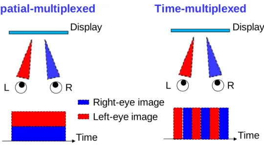
Two views
The 2D multiplexed displays, including spatial-multiplexed and time-multiplexed display, are shown in Fig. 1-4. The spatial-multiplexed type 3D displays show the left and right images at the same time, and the time-multiplexed type show the left and right images sequentially. In general, multiplexed displays consist of the optical components and liquid crystal displays (LCDs). Optical components are used to project separate images for right or left eye.
Spatial-multiplexed
Time
L
R
Display
Time-multiplexed
Time
L
R
Display
Left-eye image
Right-eye image
6
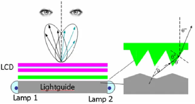
For the time-multiplexed method, many kinds of optical configuration have been proposed [7],[8],[9]. One idea is that light is reflected to the certain direction due to total internal reflection (TIR) in the double-sided prism sheet, as shown in Fig. 1-5[10]. The parallax images are formed by switching two light sources sequentially. Therefore, the left and right images can be seen by correct eye to form the 3D image.
For the spatial multiplexed method, the optical components, such as parallax barrier (Fig. 1-6(a))[11] or lenticular lenses array (Fig. 1-6(b))[12], are used to separate the left and right images into different direction.
7
R
L
R
L
R
L
Parallax Barrier
R
L
R
L
R
L
Lenticular Array
(a) (b)Fig. 1-6 Spatial multiplexed displays: (a) parallax barrier and (b) lenticular lenses.
Although time-multiplexed displays have no alignment issues and reduction of resolution, their major drawback is the flicker phenomena and it requires fast response time liquid crystal display panels. On the other hand, the spatial multiplexed 3D displays have disadvantages of lower resolution and poor alignment issues. Despite this issue, they can combine optical films with regular LCDs to form a 3D display. Therefore, spatial multiplexed type technology is applied for many 3D products.
8
Multi views
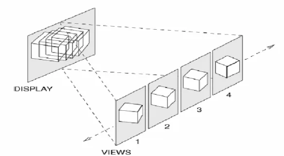
As previously mentioned, the multiplexed displays only form two views for left and right eye. When an observer moves his head slightly, he will see an incorrect 3D image. The viewing freedom of a 3D display is a key requirement in certain applications, such as public information kiosks. In order to get more natural 3D perceptible images, multi-view 3D displays (Fig. 1-7), which provide viewing freedom by generating multiple simultaneous viewing windows, were proposed. Multi-view displays can support more than one observer if enough horizontal viewing freedom is available.
Fig. 1-7 Principle of multi-view 3D displays.
Although multi-view methods can generate more natural 3D images, there are several disadvantages, such as dark lines between each view, image-flipping artifact, and decreased horizontal resolution of the images. To overcome these problems, Philips proposed an approach to multi-view LCD display based on slanted lenticular lenses array, as shown in Fig. 1-8[13]. Using slanted lenticular lenses array which is at
9
an angle to the LCD pixel array produces a balanced resolution between horizontal and vertical direction, rather than just splitting the display horizontally into many views.
Fig. 1-8 The slanted arrangement of the lenticular lenses and pixels in the Philips multi-view display.
10
1.4 Motivation and objective of this thesis
3D displays have been used in many applications, such as medical treatment, cinema, and video games. However, these 3D displays still encounter several issues that need to be improved. The crosstalk issue of 3D displays with slanted lenticular lenses is more serious than that of the one with parallax barrier. To overcome the issue, parallax barriers are used instead of lenticular lenses. However, a drawback of conventional multi-view parallax barrier 3D displays is lower transmittance with unbalanced brightness for each view. This is due to the fact that the spatial multiplexed autostereoscopic displays consist of optical component and conventional LCDs. In this conventional configuration the pixel design is optimized for normal viewing direction. Therefore, NEC proposed a 3D two-view autostereoscopic display with a novel pixel arrangement, called horizontally double-density pixels (HDDP) in 2004[14]. However, NEC did not change the pixel structure, only changed the pixel arrangement of the array.
In this research thesis, we took into account the developments done by other researchers including NEC’s above and augmented them not only to achieve more than 60% increase in transmittance, but also optimize and balance the overall brightness across all the views. We then demonstrated the proposed pixel design specifically for 6-view 3D mobile displays.
11
1.5 Organization of this thesis
The thesis is organized as following: the theory of multi-domain vertical alignment displays with optical films is presented in Chapter 2. Additionally, this chapter also represents the phase retardation at oblique incidence. In Chapter 3, the pixel designs and simulations are introduced in detail. The fabrication process of array and the measurement instruments used to characterize the performance of display system are described in Chapter 4. After that, the measurement results and the discussion are presented in Chapter 5. Finally, the conclusions and future works are given in Chapter 6.
12
Chapter 2
Principles of LCDs with Optical Films
This chapter covers the principle of multi-domain vertical alignment (MVA-b) liquid crystal cell used for our pixel design and also the principle of optical films at oblique incidence. First, the optical properties of VA cells will be discussed. Second, in order to design pixels for multi-view 3D displays, which involved oblique incidence, phase retardation at oblique incidence will then be considered. Third, the MVA-b LCDs used for conventional 3D displays are discussed. Finally, a brief summary will be given.
2.1 Optical properties of VA cells
Vertical alignment of liquid crystals with negative Δε is widely used in display applications. In a vertically aligned LC cell, the LC director is perpendicular to the surfaces of the cell. When the voltage is turned OFF, most of the liquid crystal molecules align vertically to the substrate. When an electric field is applied to the LC cell, the LC molecules are re-aligned by the electric field. In order to understand the transmission of LCDs, Jones matrix method[15] is needed to describe the propagation of light through the display. The formula for transmission of VA cell sandwiched between a pair of crossed polarizers is derived below[16]. When a plane wave is incident to a uniaxial liquid crystal layer, there are two transmission propagation modes, the ordinary mode and the extraordinary mode, which are mutually orthogonal. The refractive index of uniaxial LC for ordinary and extraordinary wave are denoted as n o
13 ⊥ = n no (2-1) 2 / 1 2 2 // 2 2 // ) cos sin ( ) ( θ θ θ n n n n ne + = ⊥ ⊥ (2-2)
The wave will undergo a phase retardation Γ due to the different propagation velocities of the extraordinary and ordinary rays inside the LC as shown in Eq.2-3:
d n ne( ) ) ( 2 0 − = Γ θ λ π (2-3)
where d is the thickness of the plate and λ is the wavelength of the light beam. We assume an incident beam of polarized light. A factor of
2 1
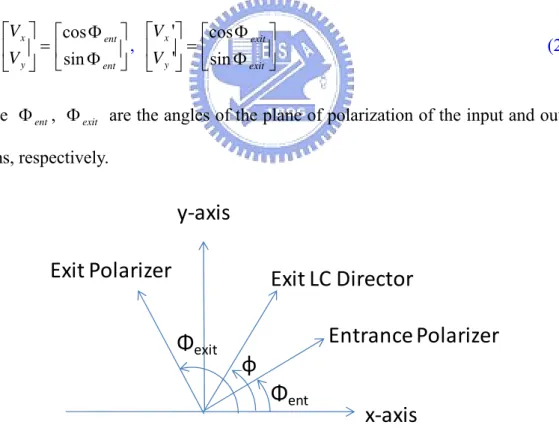
must be included for unpolarized light. We then derive the transmission properties of a general VA-LCD. Referring to Fig. 2-1, the input and output polarization states are given by Eq.2-4
⎥ ⎦ ⎤ ⎢ ⎣ ⎡ Φ Φ = ⎥ ⎦ ⎤ ⎢ ⎣ ⎡ ent ent y x V V sin cos , ⎥ ⎦ ⎤ ⎢ ⎣ ⎡ Φ Φ = ⎥ ⎦ ⎤ ⎢ ⎣ ⎡ exit exit y x V V sin cos ' ' (2-4)
where Φ , ent Φ are the angles of the plane of polarization of the input and output exit
beams, respectively.
Exit Polarizer
y‐axis
x‐axis
Entrance Polarizer
Exit LC Director
Φ
exitΦ
entφ
Fig. 2-1 Schematic drawing showing the orientation of the polarizer axes, LC directors of a general VA-LCD in the xy plane.
14
The transmitted intensity can be written
ent exit ent exit ent exit ent exit X X X X X T Φ Φ − − Φ + Φ − + Φ Φ − + Φ + Φ − = 2 cos ) ( 2 cos sin ) ( 2 sin 2 sin 2 2 sin ) ( 2 sin sin ) ( cos 2 2 2 2 2 φ φ φ φ φ φ (2-5) where 2 2 2⎟⎠ ⎞ ⎜ ⎝ ⎛ Γ + = φ X
For VA-LCD sandwiched between a pair of crossed polarizers under unpolarized light, 0
=
φ , then the Eq.2-4 should be rewritten to Eq.2-5: ⎟ ⎠ ⎞ ⎜ ⎝ ⎛ Γ Δ = 2 sin 2 sin 2 1 2 φ 2 T (2-6)
where Δ is the twist angle relative to the transmission axis of the polarizer, and Γ is φ the phase retardation of the LC cell.
2.2 Phase retardation at oblique incidence
The phase retardation may depend on the direction of propagation due to the fact that refractive index for the extraordinary mode is related to the direction of propagation. In this section, we discuss the dependence of the phase retardation on the direction of incidence.
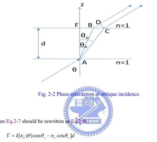
Referring to Fig. 2-2, we assume a plate of homogeneous and uniaxially birefringent medium with its c axis parallel to the plate surface. Let θe, θo be the ray angles and ne(θ), n be the eigen indices of refraction for the rays. o
The phase retardation is given by Eq. 2-7 AC kn kBD AB kne + − o = Γ (θ) (2-7)
15
where k is the wave number in vacuum.
Using the continuity condition (Snell’s law)
o o e e n n θ θ θ θ ( )sin sin sin = = (2-8)
d
F
A
B
C
θ
oθ
eD
θ
n=1
n=1
z
Fig. 2-2 Phase retardation at oblique incidence.
then Eq.2-7 should be rewritten as Eq.2-9: d n n k[ e(θ)cosθe− ocosθo] = Γ (2-9)
Fig. 2-3 shows a plate of uniaxial crystal, whose c axis is parallel to the surface. For small angles of incidence θ <<1, the phase retardation (Eq.2-9) can be written as Eq.2-10: ⎥ ⎥ ⎦ ⎤ ⎢ ⎢ ⎣ ⎡ ⎟⎟ ⎠ ⎞ ⎜⎜ ⎝ ⎛ + − + Γ = Γ θ 2φ 2 2 cos 2 sin 1 e o e e o o o n n n n n n (2-10)
where Γ is the phase retardation at normal incidence, θ is the angle between o
incidence and the normal to the plate, and φ is the angle between the c-axis and the projection of the incident wave vector onto the surface of the medium.
16
In a c plate of uniaxial crystal, whose c axis is perpendicular to the surface, the phase retardation can be written as Eq.2-11:
θ 2 sin 2 o e e o o n n n n + Γ = Γ (2-11) θ c φ
17
2.3 Conventional MVA-b LCDs
2.3.1 Pixel
Vertical alignment LC cell offers excellent contrast ratio and low operation voltage. However, a major problem is that its viewing angle is limited to ± 20°. To improve the viewing angle, several approaches to achieve multi-domain vertical alignment (MVA-b) have been developed[17],[18],[19]. Fig. 2-4(a) shows the MVA-b for mobile device, and Fig. 2-4(b) shows the cross-section of the MVA-b pixel. The protrusion (bump) was formed before coating the alignment layer. The domains are automatically controlled by the fringe fields generated near the edges of the pixel electrode and slope of bump without rubbing.
CF TFT Fringe field bump BM ITO (a) (b)
Fig. 2-4 (a) MVA-b pixel layout and (b) cross-section of the MVA-b pixel.
When the voltage is turned OFF, most of the liquid crystal molecules align themselves normal to the substrate, but those positioned above the bump incline slightly towards the substrate due to the slope of the bump beneath them. Since the
18
contrast ratio is determined by the light leakage in the voltage-off state, the light leakage near the bump is blocked by BM to enhance the contrast ratio. When the voltage is turned ON, the molecules on the sloped protrusions and those on the edge of pixel electrode initially start tilting.
2.3.2 Optical films
The MVA-b cell has the advantage of wider viewing angle. A typical optical film for MVA-b display consist of two crossed polarizers, two quarter-wave plates, and negative c plates, as shown in Fig. 2-5[20]. In general, a quarter-wave plate can convert a linearly polarized light into an elliptically polarized light and vice versa. The role of negative c plate is to significantly improve the contrast ratio.
Fig. 2-5 The optical configuration of conventional MVA-b mode.
For a beam of light with normal incidence, the phase retardation is zero for the propagation along the c axis. For a beam of light with an oblique incidence, the VA cell thus exhibits birefringence. The phase retardation increases with the angle of incidence θ . Adding a negative c plate with its c axis aligned along the z axis does not create any
19
additional phase retardation for the normal incident light. Moreover, MVA-b cell can be compensated by negative c plate for light at oblique incidence, as shown in Fig. 2-6.
no no
ne
‐ C plate
θ
Fig. 2-6 Phase retardation with negative c plates.
2.4 Summary
The VA and MVA-b mode LCDs have been briefly discussed in this chapter. We presented the fundamental theory of conventional LCDs with optical films. The basic working principle and the brief numerical calculation of VA LCDs were presented. Moreover, the formulas of phase retardation at oblique incidence for a plate and c plate were described. Additionally, the conventional pixel design of MVA-b LCDs was discussed. In this thesis work, these fundamental working principles are employed for designing the special pixel used for our proposed 3D display to enhance the brightness.
20
Chapter 3
Pixel
Design
and
Simulation
for High Transmittance of 3D Displays
This chapter covers pixel design and simulation results. First, the issues of conventional 3D displays are discussed. Second, three parameters which affect the brightness will be considered. After that, the concept of proposed pixel design and simulation results will be shown respectively.
3.1 Issues of conventional 3D displays
As mentioned in Chapter 1, there are still many limitations for different kinds of 3D technologies. For multi-view autostereoscopic 3D displays with slanted lenticular lenses, they have the issue of the higher crosstalk compared to parallax barrier.
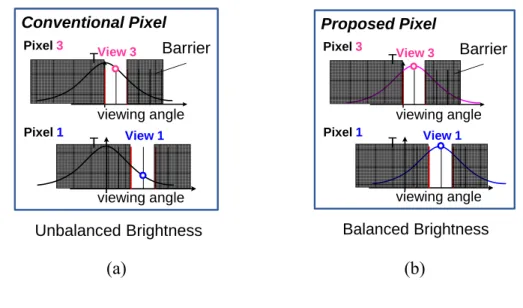
However, a drawback of conventional multi-view slanted parallax barrier 3D displays is lower transmittance with unbalanced brightness for each viewing zone. This is due to the fact that the pixel design of conventional LCDs was optimized for normal viewing direction. In a conventional 3D display with many viewing zones, image transmittance away from the normal direction is too low. Here we designed a pixel array based on a 6-view slanted parallax barrier 3D display, the pixels can be considered to be comprised of 6 kinds of pixels, as shown in Fig. 3-1. The schematic drawing of conventional parallax barrier display with unbalanced brightness issue is shown in Fig. 3-2. Fig. 3-3(a) shows the transmittance curve of a conventional liquid crystal display with parallax barrier. The light from pixel 1 is too low in viewing zone
21
1. If there are more than 6 viewing zones, the transmittance at a large viewing angle is significantly lowered. Therefore, unbalanced brightness issue for each viewing zone occurs in conventional 3D displays.
The design concept is that each kind of pixel has its own transmittance curve whose maximum transmittance can be optimized within its own viewing zone. For instance, the maximum transmittance of pixel 1 is in viewing zone 1, as shown in Fig. 3-3(b). More light passes through the LC cell within viewing zone 1. Other kinds of pixels can also be optimized for their viewing zones, the transmittance at wide viewing angles can be increased, and the difference in brightness between each viewing zone can be minimized.
6
5
4
3
2
1
3
4
5
6
2
1
3
4
5
6
2
1
3
4
5
6
2
1
Fig. 3-1 6-view slanted parallax barrier 3D display.
5 3 6 4 21 3 4 5 6 2 1 6 views
22 viewing angle TView 3 Conventional Pixel viewing angle T View 1 Barrier Pixel 3 Pixel 1 Unbalanced Brightness viewing angle TView 3 Proposed Pixel viewing angle T View 1 Barrier Pixel 3 Pixel 1 Balanced Brightness (a) (b)
Fig. 3-3 Transmittance of (a) conventional LC and (b) proposed LC.
3.2 Parameters affecting brightness of 3D displays
There are three major parameters which affect the brightness of 3D displays. The configuration of a typical autostereoscopic 3D display is shown in Fig. 3-4. When considering the brightness of displays, the first parameter is the transmittance curve of the liquid crystal cell. We thus proposed a single domain VA with different LC alignment for different kinds of pixels, the detailed results are discussed in section 3.3. The second parameter is the aperture ratio of the pixel array, which is considered in section 3.4. The aperture ratio can be increased by using a single domain VA cell without a bump. The third parameter that should be considered is the aperture ratio of parallax barrier in section 0. By considering these three parameters, total brightness can be increased. The total brightness, which is determined by these three parameters, is written as ) .( . ) .( . ) (LC AR pixel AR barrier T Ttotal = × × (3-1)
23
Fig. 3-4 The configuration of the parallax barrier 3D display.
3.3 Single domain VA
In conventional LCDs, the wide viewing angle is a critical issue to be improved. Many researchers focused on wide viewing angle issue for either large panel liquid crystal displays or handheld displays, as depicted in Fig. 3-5(a). One of the wide viewing angle technologies is multi-domain VA. However, when combining with parallax barriers to form a 3D display, most of the light from pixel is blocked by parallax barriers, the light can only pass through at specific viewing zone, as shown in Fig. 3-5(b). Therefore, the objective of our design is to enhance the brightness at specific viewing angles, as shown in Fig. 3-5(c). The reason to use single domain VA is that single domain VA can generate higher transmittance than MVA-b mode in a specific viewing zone, as illustrated in Fig. 3-6. Fig. 3-7 shows that each kind of pixels has a transmittance curve optimized for its own viewing zone in 6-view 3D display. Under above-mentioned design concept, each pixel has maximum transmittance in its
24
viewing zone, so the total transmittance in large viewing angle can be increased. Furthermore, the difference in brightness between each view can be minimized. We proposed two methods that could generate a peak of transmittance curve at specific viewing angles with different gray levels in the following section.
Conventional Display Conventional Display + Parallax Barriers
Single‐domain Display
(a) (b) (c)
Fig. 3-5 Viewing angle of (a) conventional displays, (b) conventional 3D displays, and (c) single domain displays.
Single domain
Multi‐domain
LC alignment
25
0
10
20
‐20 ‐10
T
(a
.u
.)
viewing angle (Deg.)
pixel 1
pixel 2
pixel 3
pixel 4
pixel 5
pixel 6
Fig. 3-7 Each kind of pixel can be optimized for specific viewing zone.
3.3.1 Changing the thickness of negative c plate VA
The optical configuration of single domain vertical alignment is shown in
Fig. 3-8. The total phase retardation is given by Eq.3-2:
) ( ) ( 2 ) ( ) ( θ θ λ π θ θ =ΓLC + Δn deff Γ (3-2)
where deff is the effective thickness of the c plates.
The second term of Eq.3-2 is caused by negative c plate. By changing the thickness of the negative c plate, we can generate the maximum transmittance in a specific viewing zone. Fig. 3-9 shows an example of this method.
26
Fig. 3-9 Maximum transmittance can be generated at a specific viewing angle by changing the thickness of the negative c plate.
Assume that the maximum transmittance is at viewing angle θA. From Eq.2-6,
the maximum transmittance can be generated at viewing angle θB by increasing the
thickness of the c plate. Fig. 3-10 shows the simulated transmittance profile with various kinds of pixels with different LC alignment directions and c plate thicknesses by DIMOS[21]. The transmittance at viewing zone 6 (-9°) was enhanced with different gray levels compared to that of the conventional pixel layout. The difference in brightness between each viewing zone was minimized. However, it is difficult to fabricate due to the different thickness of c plate for different kinds of pixel. Therefore, we proposed the second method, Normally White Single Domain Vertically Alignment, to enhance transmittance at each viewing zone.
27
Multi-domain VA Transmittance profile (Bright state) Single-domain VA Transmittance profile (Bright state) Single-domain VA Transmittance profile (Gray level state)
-9°
-6°
-2°
(a) View 6 (-9°) (b) View 5 (-6°) (c) View 4 (-2°)
2°
6°
9°
(d) View 3 (2°) (e) View 2 (6°) (f) View 1 (9°)
Fig. 3-10 Transmittance profiles of single-domain VA and conventional MVA-b for different kinds of pixels.
28
3.3.2 Normally White Single Domain VA
The optical configuration of Normally White Single Domain VA with different azimuth angles is shown in Fig. 3-11. According to section 2.2, the light at oblique incidence in optical films, the maximum transmittance can be generated in a specific viewing zone by rotating the angle Φ. Fig. 3-13 shows a simulated transmittance profile with various kinds of pixels with different LC alignment directions (Fig. 3-12).
Fig. 3-11 The optical configuration of Normally White Single Domain VA.
3
4
5
6
2
1
6
5
4
3
2
1
3
4
5
6
2
1
3
4
5
6
2
1
110
104
95
275
281
290
Φ
29
Multi-domain VA Transmittance profile (Bright state) Single-domain VA Transmittance profile (Bright state) Single-domain VA Transmittance profile (Gray level state)
(a) View 6 (-9°) (b) View 5 (-6°) (c) View 4 (-2°)
(d) View 3 (2°) (e) View 2 (6°) (f) View 1 (9°)
Fig. 3-13 Transmittance profiles of Normally White Single Domain VA and conventional MVA-b for different kinds of pixels.
30
The transmittance comparison of each view is shown in Fig. 3-14. The relative improvement in transmittance on the bright state is 7%. Due to the fact that the total viewing range of a 6-view slanted parallax barrier 3D display is only 18°(-9°~ 9°), the transmittance is not enhanced enough compared to that of a conventional one. If number of views increase, our design also can generate the maximum transmittance at wide viewing points. Fig. 3-14 also shows the transmittance at large viewing points (~30°), the transmittance could be enhanced by more than 24%. Furthermore, the difference in brightness between each view would be minimized.
0.2 0.22 0.24 0.26 0.28 0.3 0.32 0.34 ‐30 ‐20 ‐9 ‐6 ‐2 2 6 9 20 30
Tr
an
sm
it
tan
ce
(a.
u
.)
Viewing angle(deg.)
6‐view slanted barrier Conventional (Bright state) Single Domain (Bright state)Fig. 3-14 The transmittance comparison of Normally White Single Domain VA and conventional MVA-b for each view.
31
3.4 Pixel array design
A parallax barrier 3D display with conventional MVA-b pixel design is shown in Fig. 3-15. There are two major opaque components, including storage capacitor (Cst)
and bump, within the barrier slit (pink region), so the aperture ratio of the pixel within the pink region is low. We proposed a pixel layout which increases the brightness of 3D display and suppresses the crosstalk issue. The brightness can be increased due to bumpless pixel with slanted storage capacitor. Beside, the crosstalk issue can be suppressed due to pixel with slanted storage capacitor.
Fig. 3-15 A parallax barrier 3D display with conventional MVA-b pixel design.
3.4.1 Bumpless
The conventional MVA-b pixel design was discussed in section 2.3. The bump is needed to achieve multi-domain alignment. Due to the fact that the light leakage near the bump is large, there should be a black matrix to block the light around the bump. According to section 3.3.2, transmittance of each kind of pixel in its own viewing zone could be enhanced by using Normally White Single Domain VA. Due to the fact that the LC mode is single domain in our design, there is no bump in the pixel layout.
32
Therefore, the aperture ratio can be increased by removing the bump.
In the proposed Normally White Single Domain VA method, each kind of pixels has its own ITO slit direction which can control LC alignment. The direction of LC pre-alignment will be the same as that of ITO slit by PSA technology[ 22 ]. Consequently, different kinds of pixels have their own LC pre-alignment. Fig. 3-16 shows the simulation results of the conventional MVA-b mode and NW single domain VA for the 6th pixel with an azimuthal angle of LC alignment 110° by using ExpertLCD[23]. The aperture ratio of pixel is increased by a factor of 1.16 compared to that of the conventional pixel.
AR=45% AR=52%
(a) (b)
Fig. 3-16 The 6th pixel layout of (a)conventional 2.83” MVA-b mode (b) NW single
domain VA with azimuth angle of ITO fine slit 110°.
3.4.2 Slanted storage capacitor
According to Fig. 3-15, the second significant opaque component is storage capacitor which was not optimized for slanted parallax barrier. We modified the shape of the storage capacitor from rectangular to slanted structure. After that, the slanted storage capacitor is rearranged to hide behind the parallax barrier in order to increase
33
the aperture ratio of pixel within the barrier slit (pink area), as shown in Fig. 3-17.
Fig. 3-17 A parallax barrier using proposed pixel with slanted storage capacitor.
In addition, the crosstalk can be minimized due to optimizing the position of storage capacitor. Fig. 3-18 shows viewing zone 3 of a conventional 3D display. In the viewing zone 3, there is interfering light, called crosstalk[24], from pixel 2 and pixel 4. By optimizing the position of storage capacitor to block the light leakage from pixel 2, crosstalk can be minimized.
34
3.5 Aperture ratio of parallax barrier
This is a joint work between classmates in National Tsing Hua University (NTHU). The parallax barriers were designed by NTHU. The aperture ratio of the parallax barrier is determined by the barrier slit size. The barrier slit size can be increased by Normally White Single Domain VA with slanted storage capacitor (section 3.3.2 and section 3.4), as shown in Fig. 3-19. From Fig. 3-20, the aperture ratio of parallax barrier has a 60% improvement compared to that of conventional 3D displays based on the same crosstalk condition[25].
Fig. 3-19 The modified pixel layout.
Aperture ratio of barrier (NTHU)
8.9%
14.3%
~60%
35
3.6 Discussion
Our task is to design a 6-view 2D/3D switchable display based on single domain VA for the same resolution in 2D and 3D images. The reason for the same resolution in 2D and 3D images is shown in Fig. 3-21. In 2D mode, as shown in Fig. 3-21(a), the six types of pixels are written by the same image signals. In 3D mode, as shown in Fig. 3-21(b), the six types of pixels are written by six types of image signals, respectively. In order to get acceptable 2D images, the resolution of images in 2D mode should be the same as that of images shown in conventional LCDs. Consequently, the pixel size of proposed method should be smaller than conventional pixel size. For a 6-view 3D display, the pixel size should be 1/6 compared to conventional pixel size, as shown in Fig. 3-21(c). However, it is not easy to increase the pixel density due to requirement of more driving control lines and ICs. Therefore, for fabrication, we used multi-domain instead of single domain VA to keep the advantage of wide viewing angle and high resolution in 2D mode. The multi-domain mode with slanted storage capacitor ( Fig. 3-22) has been fabricated and will be discussed in Chapter 5.
1 1 1 1 1 1 1 1 1 1 1 1
2D Image(multi-domain) 3D Image(single domain)
4 3 2 1 5 6 3 2 4 5 1 6 Proposed Conventional LC alignment
(a) 2D mode (b) 3D mode (c) pixel size
36
Fig. 3-22 Pixel layout for fabrication.
3.7 Summary
Three parameters, which include transmittance of LC cells, the aperture ratio of pixels, and the aperture ratio of the parallax barrier, affecting the brightness of 3D displays, were discussed (Table 3-1). In the LC cell, we used Normally White Single Domain VA to optimize the transmittance at a specific viewing zone. The relative improvement in transmittance was about 7%. The aperture ratio of the pixel was improved by 16% compared to that of conventional pixel layout. The relative improvement of the aperture ratio of the parallax barrier was about 60% based on the same crosstalk condition. Finally, the brightness of the proposed pixel (Fig. 3-19) is increased by a factor of 2 compared to that of conventional 3D displays, as shown in Table 3-1.
In the fabrication, we utilized the multi-domain vertically alignment pixel layout with the slanted storage capacitor, the brightness of the fabricated pixel increased by a factor of 1.46 compared to conventional 3D displays (Table 3-1).
37
Table 3-1 The improvement of each factor.
LC Design Pixel Design
Brightness Enhancement
Single
Domain Slanted Cst Bumpless
Combined Effect of Factor 1 & 2
Barrier A.R. (%) 118 136 160
LC Trans. (%) 107 - - 107
Pixel Array A.R. (%) - - 116 116
38
Chapter 4
Fabrication Technologies
and Measurement Instruments
The techniques utilized to fabricate the designed pixel array will first be described. After that, the measurement instrument, Conoscope, which is used to characterize the image performance of LCDs will be discussed.
4.1 Fabrication process
The fabrication process flow of TFT LCDs is shown in Fig. 4-1. In the process flow, TFT LCDs can be separated into two major parts: the array and color filter substrates. After fabricating the array and color filter substrates respectively, these two substrates are assembled by the cell process. The TFT-LCDs will be fabricated after the module process, which includes the backlight modules and driving control ICs. The fabrication process, including array, color filter, and cell process will be discussed in more detail.
Bottom Substrate Top Substrate
Array Process CF Process
Cell Process
Module Process
LCD Panel LTPS
39
(a) Array process
In the pixel array fabrication process, Low Temperature Poly-Silicon (LTPS) technology for thin-film-transistor liquid crystal display (TFT-LCD) panels is used for information devices such as mobile displays and personal digital assistants (PDAs). Poly-Si TFTs have much higher electron mobility than a-Si TFTs. Consequently, poly-Si TFTs with the same channel geometry as a-Si TFTs allow for a considerably larger current. In other word, if carrying the same current as a-Si TFTs, the area of poly-Si TFTs is smaller within a pixel. For this reason, displays with a high pixel density are addressed by poly-Si TFTs, as they deprive the pixels of the least amount of transparent area. Fig. 4-2 shows fabrication steps of top-gate LTPS TFTs.
(1) An a-Si:H film is deposited by Plasma Enhanced Convention Vapor deposition system (PECVD) and later patterned by dry etching. After that, SiO2 layer, gate dielectric, is deposited.
(2) Thin a-Si layer is crystallized by laser annealing, a low temperature process not exceeding a substrate temperature of 450°C to form a poly-Si layer. Then, gate electrode is formed by sputtering and patterning process.
(3) P+ poly-Si is formed by ion implantation in order to yield low resistance drain and source contacts. A SiO2 passivation layer is deposited on top of the
gate later.
(4) The via holes for the drain and source contacts are etched down to poly-Si, which is followed by sputtering and patterning of metals, such as Al, for the drain and source contacts.
40 Substrate SiO2 Channel a-Si:H Gate oxide Substrate SiO2 Channel Gate Poly-Si Gate oxide Interlayer oxide Substrate SiO2 Channel Gate Cr/Al Gate oxide Drain Source Interlayer oxide Substrate SiO2 Channel Gate p+-poly-Si Gate oxide
Fig. 4-2 Fabrication steps for top-gate poly-Si TFTs[26].
(b) CF process
The process of the color filter substrate is divided into two major parts: black matrix and color pixels for red, green, and blue. The first step is the deposition and patterning of the black matrix. Second, the color pixels for red are developed by deposition of the pigment dispersed color material which is exposed to UV light. Afterward, color pixel for green and blue are formed by repeating the second step.
41
(c) Cell process
After fabricating the array and color filter substrates respectively, these two substrates are assembled by the cell process. First, photo spacers are fabricated on color filter substrate. The function of the photo spacers is to maintain cell gap and prevent short circuit connection of top and bottom electrodes. The LC cell is assembled by sealing the color filter and array substrates.
The LC predetermined alignment is controlled by Polymer Sustained Alignment technology (PSA), which has been proposed by Fujitsu[22]. Fig. 4-3 shows the fabrication process to form the polymer layer, which can control LC alignment. PSA technology can be divided into four steps:
(1) Appropriate concentration of UV curable monomer is added to liquid crystal and injected to cell.
(2) By applying voltage, liquid crystal will reorient due to the electric field.
(3) LC cell is irradiated by UV light to form polymer layers on the inner surface of the substrate.
(4) Finally, LC has stable predetermined alignment after removing voltage. Therefore, the initial liquid crystal alignment can be obtained by PSA process.
42 V UV V ITO PI Monomer Polymer layer
Fig. 4-3 Fabrication process of polymer layer[22].
4.2 Measurement instruments
Conoscope was used to measure the luminance of LCDs. The Conoscope (Fig. 4-4) can be used for evaluation of the characteristics of LCDs, including luminance vs. viewing direction, chromaticity vs. viewing direction, response time, electro-optical characterization, etc. The basic principle of Conoscope is depicted in Fig. 4-5. A transparent sample that is illuminated from the back side via a cone of light beams C is located in the front of focal plane of the lens L1. The light through the sample is collected simultaneously over a large solid angle by the lens L1 and generate a pattern IF1 in the rear focal plane F’1 of the lens L1. In the pattern IF1, the intensity of each area element corresponds to the intensity of one elementary parallel beam with a specific direction of light propagation. The directional intensity distribution of the cone of elementary parallel light beams C is transformed into a two-dimensional distribution
43
of light intensity and color with each location in the pattern IF1 corresponding to exactly one direction of light propagation (θ, φ).
A second optical system L2 optionally projects the figure IF1 on a two dimensional detector array such as a Charge-coupled Device (CCD) for evaluation of the spatial intensity distribution, which corresponds to the directional intensity distribution of the light emerging from the measuring spot on the sample.
Fig. 4-4 Conoscope.
44
Chapter 5
Measurement Results and Discussion
5.1 Introduction
The objective of the measurement is to investigate the brightness of the 3D displays with different pixel layouts. We demonstrated the 2.83” 6-view parallax barrier 3D display. According to the simulated results presented in Chapter 3, Table 5-1 shows the specifications of the parallax barrier and 2.83” LCDs with conventional and proposed pixel layouts. The proposed pixel layout is multi-domain vertically alignment mode with slanted storage capacitor. The measurement results will be shown in this chapter.
5.2 Measurement results and discussion
The measurement results can be categorized into two parts: brightness and crosstalk. The conventional and proposed pixel images were observed by optical microscope, as shown in Fig. 5-1.
45
Table 5-1 Specifications of the parallax barrier and 2.83” LCDs.
Conventional 3D Display Proposed 3D Display Parallax Barrier Slit (μm)
(by NTHU) Spatial Freq.=180μm/cycle 26 19 Pixel Layout (30μm X 90μm) Resolution 640 X 480 640 X 480
Thickness of Glass Substrate
(μm) 300 500
Thickness of Polarizer (μm) 180 180
Conventional MVA-b Proposed Pixel with
Slanted Cst
Pixel Images (Multi-domain VA)
46
5.2.1 Brightness
The brightness increase ratio of the 3D display with pixel which has slanted storage capacitor is shown in Table 5-2. The brightness of 2.83” 3D display with the slanted storage capacitor improves by 63% compared to that of the conventional 3D display. For the aperture ratio of the parallax barrier, the increase ratio by measurement is higher than that of the design due to fabrication variation. The parallax barrier was fabricated by printing process with 20000dpi. The brightness of the proposed LCD is increased due to increasing the aperture ratio. These measurement results imply that the brightness of 3D display with proposed pixel design is increased compared to conventional 3D display.
Table 5-2 Brightness increase ratio of the proposed pixel layout compared to 3D display with conventional MVA-b pixel layout.
Simulation Measurement
A.R. of Barrier (%) 136 152
Brightness of LCD (%) 113 107
47
5.2.2 Crosstalk
The crosstalk of each view was measured by inputting the patterns (Fig. 5-2). For instance, Fig. 5-3 shows how to measure the crosstalk of viewing zone 5 and 3 resulted from the light leakage from pixel 4. The input pattern, BBWBBB, represents that white image can be observed within viewing zone 4 and the rest of viewing zones show black image in the ideal case (0 % crosstalk). After inputting these six patterns (Fig. 5-2) respectively, the crosstalk of 3D displays based on conventional and proposed pixel layouts can be measured by Conoscope, as shown in Table 5-3. The results demonstrate that 3D display with proposed pixel layout has lower crosstalk even if parallax barrier slit size is wider (26μm). Therefore, the image quality of each viewing zone can be improved due to lower crosstalk.
(a)WBBBBB (b)BWBBBB (c)BBWBBB (d)BBBWBB (e)BBBBWB (f)BBBBBW
48
3
4
5
6
2
1
6
5
4
3
2
1
3
4
5
6
2
1
3
4
5
6
2
1
B
B
W
B
B
B
Light leakage from pixel 4
Fig. 5-3 The illustration of measurement of inputting the test pattern (BBWBBB).
Table 5-3 Crosstalk was measured by Conoscope.
Conventional Slanted Cst
Barrier Slit Size (μm) 19 26
Crosstalk (%) ~51 ~37
5.3 Summary
For the brightness and crosstalk, the comparisons of conventional MVA-b and proposed pixel with slanted storage capacitor are summarized in Table 5-4. The brightness of 2.83” 3D display with the slanted storage capacitor improves by 63% compared to that of the conventional 3D display. In addition, 3D display with proposed pixel layout has lower crosstalk even if parallax barrier slit size is wider (26μm). The results indicate that the 3D display with proposed pixel yields not only higher brightness, but lower crosstalk.
49
Table 5-4 Comparisons of 3D displays with conventional and proposed pixel layouts.
Conventional MVA-b Proposed Pixel with
Slanted Cst Brightness Increase Ratio (%) 100 ~ 163 Crosstalk (%) ~37 ~19 Images of Viewing Zone 3
50
Chapter 6
Conclusions and Future Work
6.1 Conclusions
The pixel layout for multi-view 3D display has been presented and demonstrated in this thesis. There are three parameters: transmittance of LC cells, the aperture ratio of pixels, and the aperture ratio of the parallax barrier, affecting brightness of 3D displays. We proposed Normally White Single Domain VA with slanted storage capacitor to increase the brightness and suppress the crosstalk. The simulated results indicate that the brightness is increased by a factor of 2 compared to that of a conventional 3D display with parallax barrier. The unbalanced brightness issue can be minimized by utilizing Normally White Single Domain VA mode LC cell.
The pixel layout we fabricated is multi-domain vertically alignment mode with slanted storage capacitor. The simulated results show the brightness of the parallax barrier 3D display with slanted storage capacitor pixel layout is increased by a factor of 1.6. The measurement results (brightness increase ratio~1.6) are close to simulation result. In addition, the 3D display with proposed pixel layout has lower crosstalk even if parallax barrier slit size is wider (26μm). In conclusion, the 3D display with proposed pixel yields not only higher brightness but lower crosstalk.
The proposed pixel layout can also be applied for large size of 3D display to enhance the brightness due to the fact that the position and shape of the storage capacitor were optimized for the shape of barrier, as shown in Fig. 3-20. The capacitor was hided behind the barrier to increase the aperture ratio within the barrier slit.
51
6.2 Future work
Nowadays, the major issues of mutli-view 3D displays are lower brightness and lower resolution of each view. In this thesis, we proposed a pixel layout which is applied for 3D displays to obtain higher brightness with lower crosstalk. However, the aperture ratio of the pixel will decrease as increasing the resolution. After combining with parallax barrier, the brightness is degraded significantly.
In this thesis, although the brightness of a 3D display with the proposed pixel layout is increased, much light is still blocked by opaque components, such as data lines. The pixels consist of straight data lines, while the parallax barrier is slanted. Fig. 6-1 shows the concept of the slanted pixel which has higher aperture ratio of effective area due to slanted data lines. Slanted data lines have the same angle as slanted parallax barrier, therefore the light from the pixels become more. Moreover, the crosstalk issue can be degraded effectively due to the light form neighboring pixel become less. As increasing the resolution of each view, slanted pixel has higher brightness than conventional pixel due to the fact that shape of pixel is optimized for slant parallax barrier.
52
References
[1] J. A. Castellano, Handbook of Display Technology, Academic Press, San Diego (1992).
[2] N. Holliman, 3D Display Systems, Department of Computer Science, University of Durham, 3, Feb. (2005).
[3] B. Lane, Proc. SPIE, 0367 (1982).
[4] A. Sullivan, Proc. SID’03, p.1531 (2003).
[5] P. St. Hilaire, S. A. Benton, M. Lucente, P. M. Hubel, Proc. SPIE, 1667, p.73 (1992).
[6] H. Choi, Y. Kim, S. W Cho, and B. Lee, IDW’06, p.1361 (2006). [7] K. Toyooka, T. Miyashita, T. Uchida, Proc. SID’01, p.174 (2001).
[8] T. Sasagawa, A. Yuuki, S. Tahata, O. Murakami, K. Oda, ”Dual Directional Backlight for Stereoscopic LCD”, Proc. SID’03, p.399 (2003).
[9] Y. M. Chu, K. W. Chien, H. P. D. Shieh, J. M. Chang, A. Hu, Y. C. Shiu, and V. Yang, J. Soc. Inf. Display 13, p.875 (2005).
[10] K. W. Chien and H. P. D. Shieh, Appl. Opt. 45, p.3106 (2006). [11] L. Lipton et al., Proc. SPIE, 4660, p.229 (2002).
[12] D. Takemori, K. Kanatami, S. Kishimoto, S. Yoshi, and H. Kanayama, Proc. SID’95, p.55 (1995).
[13] C. van Berkel and J. A. Clarke, Proc. SPIE, 3012, p.179 (1997).
[14] S.Uehara, N.Ikeda, N.Takanashi, M.Iriguchi, M.Sugimoto, T.Matsuzaki, and H.Asada, Asia Display/ IMID’04 Degist, p.783 (2004).
[15] R. C. Jones, J. Opt. Soc. Am. 31, p.488 (1941).
[16] P. Yeh and C. Gu, Optics of Liquid Crystal Displays, Chapter 4, J. Wiley and Sons, New York (1999).
[17] A. Takeda, S. Kataoka, T. Sasaki, H. Chida, H. Tsuda, K. Ohmuro, Y. Koike, T. Sasabayashi, and K. Okamoto, Proc. SID’98, p.1077 (1998).
[18] Y. Tanaka, Y. Taniguchi, T. Sasaki, A. Takeda, Y. Koibe, and K. Okamoto, Proc. SID’99, p.206 (1999).
[19] S. Kataoka, A. Takeda, H. Tsuda, and Y. Koike, Proc. SID’01, p.1066 (2001). [20] Q. Hong, T. X. Wu, X. Xhu, R. Lu, and S. T. Wu, Appl. Phys. Lett. 86, 121107
53
[21] DIMOS User’s Guide, autronic-MELCHERS GmbH.
[22] K. Hanaoka, Y. Nakanishi, Y. Inoue, S. Tanuma, Y. Koike, Proc. SID’04, p.1200 (2004).
[23] ExpertLCD User’s Guide, Daou Xilicon Technology Co., Ltd.
[24] H.K. Hong, S.M. Jung, B.J. Lee, H.J. Im, and H.H. Shin, Proc. SID’08, p.348 (2008).
[25] S.C. Chuang and C.H. Chen, Proc. SID’08, p.452 (2008).
[26] E. Lueder, Liquid Crystal Displays: Addressing Schemes and Electro-Optical Effects, Wiley and Sons, New York (2001).