0040-6090/02/$ - see front matter䊚 2002 Elsevier Science B.V. All rights reserved. PII: S 0 0 4 0 - 6 0 9 0 Ž 0 1 . 0 1 7 2 3 - 0
Effects of CH
4ySiH flow ratio and microwave power on the growth of
4b-SiC on Si by ECR-CVD using CH
4ySiH yAr at 200 8C
4Wen-Horng Lee , Jing-Cheng Lin , Chiapyng Lee *, Huang-Chung Cheng , Tri-Rung Yew
a a a, b cDepartment of Chemical Engineering, National Taiwan University of Science and Technology, Taipei 10672, Taiwan, ROC
a
Department of Electronics Engineering, National Chiao-Tung University, Hsinchu 30050, Taiwan, ROC
b
United Microelectronics Corporation, Science-Based Industrial Park, Hsinchu, Taiwan, ROC
c
Received 28 November 2000; received in revised form 13 August 2001; accepted 16 November 2001
Abstract
The effects of CH4ySiH flow ratio and microwave power on the formation of SiC at 200 8C by electron cyclotron resonance4
chemical vapor deposition is investigated. When the CH4ySiH flow ratio is varied from 0.5 to 10, crystalline phase of films4
vary from polycrystalline silicon to polycrystalline b-SiC, and finally to amorphous silicon carbide. However, as the microwave power increases from 300 to 1500 W, the film microstructure changes from polycrystalline Si to amorphous SiC, and finally to polycrystalline b-SiC. The deposition mechanism which controls the film characteristics is also presented. 䊚 2002 Elsevier Science B.V. All rights reserved.
Keywords: Chemical vapor deposition; Cyclotron resonance studies; Silicon carbide; Transmission electron microscopy
1. Introduction
Silicon carbide (SiC) is a promising semiconductor
material for electronic and optical devices, owing to its superior properties such as high thermal conductivity, high-melting point, high breakdown field, high saturated drift velocity, small dielectric constant, and wide band gap w1–3x. However, due to its physical stableness, chemical inertness, and hardness, it can be used as optical filter antireflection hard coatings, X-ray masks, and corrosion-resistant materials. Furthermore, SiC can also be used as a thin buffer layer for the growth of diamond films on silicon w4x and GaN films on a-Al O w5x.2 3
With rapid miniaturization of devices and circuits, significantly lower growth and processing temperatures are being sought. However, conventional ways of depos-iting SiC films by CVD methods were carried out in a high temperature environment. A high-temperature CVD process of depositing SiC films is not suitable for device
* Corresponding author. Tel.: 6611; fax: q886-2-737-6644.
E-mail address: [email protected](C. Lee).
fabrication, because it may lead to autodoping and causing non-abrupt heterojunctions between SiC and silicon. A relatively new technique, known as electron cyclotron resonance chemical vapor deposition (ECR-CVD) has the ability to deposit b-SiC (3C-SiC) at low
temperatures w6,7x.
In this study, we examine effects of CH4y SiH flow4
ratio and microwave power on the properties of SiC films.
2. Experimental
Silicon carbide (SiC) films were deposited in a commercial Plasma-Quest Model-357 ECR-CVD reactor using CH4y SiH y Ar gas mixtures. The ECR-CVD sys-4
tem configuration has been described elsewhere w8x. The substrates used were (100) oriented, p-type sili-con wafers with a resistivity of 5–15 Vcm, and in size of 15=30 mm . The substrates were ex situ cleaned by2
a modified spin-etching method w9x to provide a hydro-gen-terminated silicon surface and prevent surface oxi-dation during air exposure w10x. The substrate was then loaded into the reactor within a few minutes after cleaning.
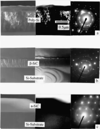
Fig. 1. XTEM dark-field and bright-field micrographs with selected-area electron diffraction patterns of the films grown at 200 8C, 1200 W, with(a) CH ySiH s0.5, (b) CH ySiH s1, and (c) CH ySiH s4 4 4 4 4 4 5.
The deposition conditions of SiC films were as follows. Ar was used as the plasma excitation gas, and CH and SiH were used as reaction gases. The total4 4
pressure, substrate temperature, Ar flow rate, and SiH4
flow rate were kept constant at 20 mtorr, 200 8C, 100 sccm, and 5 sccm, respectively. The change of CH flow4
rate varied the CH4y SiH4 flow ratio. The effect of microwave power was investigated by keeping the CH4
and SiH flow rates at 5 and 2.5 sccm, respectively. The4
deposition time was 30 min in all cases. Since the microwave power can lead to quite different self-induced temperatures without any compensation, the substrate was maintained at 200"2 8C by a resistive heater intentionally.
Crystalline structure of the deposited SiC film was examined in a JEOL 2000FX STEM. The samples used for both plan-view and cross-sectional transmission elec-tron microscopy (XTEM) inspection were cut into a
size of 2=5 mm . The XTEM is a destructive analysis2
technique to observe the deposited film with electron beams perpendicular to the sample surface, providing the information of crystalline phase and lattice constant of the deposited films.
Fourier transform infrared spectroscopy(FTIR) spec-tra were obtained with a BIO-RAD FTS-40 spectrometer from 400 to 4000 cmy1, with a resolution of 4 cmy1
and 16 scan times. XPS analyses were performed in a VG Microtech MT-500 spectrometer. The spectrometer was equipped with a hemispherical analyzer and all X-ray photoelectron spectroscopy (XPS) data presented
here were acquired using the MgKa X-rays (1253.6
eV). Peak positions were calibrated with respect to the
C1s peak at 284.6 eV from the adventitious hydrocarbon contamination. The compositionX of the deposited film (SiC ) can be evaluated from the ratio of the C1s toX
Si2p peak areas corrected by suitable sensitivity factors of S s0.27 and S s0.25 w11x. Rutherford backscatter-Si C
ing spectroscopy (RBS) was performed in a Canberra Series 35 Plus spectrometer using 2.0 MeV helium ions, and a backscattering angle of 1708.
3. Results and discussion
An appropriate CH4y SiH flow ratio is crucial for4
crystalline SiC formation according to our results. Fig. 1 shows the XTEM dark-field and bright-field micro-graphs with electron diffraction patterns of the films grown at 200 8C, 1200 W, and various CH4y SiH flow4
ratios from 0.5 to 5. Fig. 1a shows that at a CH4y SiH4
flow ratio of 0.5, the deposited film on Si is of polycrystalline-Si(poly-Si) determined by the ring spac-ing of the electron diffraction pattern. When the CH4y
SiH flow ratio was increased to 14 (the same as in the
cases of flow ratios of 1.5, 2 and 4), Fig. 1b shows that the films grown are of polycrystalline structure. Using the spot diffraction pattern of the SiN100M zone in Fig.
1b as a reference, the structure and lattice constant of the film can be determined by measuring the ring spacing of the same electron diffraction pattern in Fig. 1b. The film was identified to be a zinc-blende structure with a lattice constant of 0.436"0.005 nm, which is identical to that of bulk b-SiC w12x. A plan-view TEM micrograph of the CH4y SiH s2 film is shown in Fig.4
2. The grain size of b-SiC is approximately 0.20 mm. However, amorphous SiC(a-SiC) is obtained when the CH4y SiH flow ratio is 54 (the same as in case of flow
ratio of 10), as shown in Fig. 1c.
According to the XTEM results, it is interesting to find that at 200 8C and 1200 W, polycrystalline b-SiC film can be grown as the CH4y SiH flow ratio is from4
1 to 4. Polycrystalline-Si is obtained when the CH4y
SiH flow ratio is approximately 0.5, while amorphous-4
SiC is deposited as the CH4y SiH ratio is approximately4
5 or higher. The above results were also confirmed by Fourier transform infrared (FTIR), X-ray photoelectron spectrometry(XPS), and RBS analyzes.
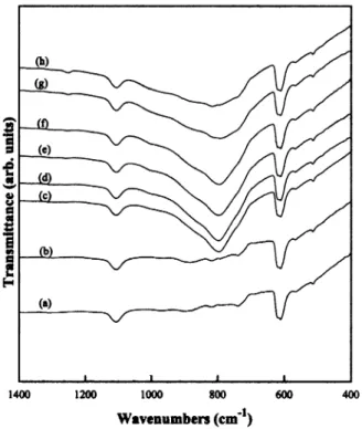
Fig. 3 shows FTIR spectra of the films deposited at various CH4y SiH flow ratios. The stretching mode of4
SiC appears at 800 cmy1 w13x. The weak peaks at
approximately 1100 and 600 cmy1 are due to SiO and
Fig. 2. Plan-view TEM micrograph of the microcrystalline b-SiC layer grown at 200 8C, 1200 W, and CH4ySiH s2.4
Fig. 4. XPS core level peaks of Si2p for the films deposited at various CH4ySiH flow ratios.4
Fig. 3. FTIR transmission spectra of the Si substrate and the films deposited at various CH4ySiH flow ratios.4 (a) Si substrate, (b) CH4ySiH s0.5,4 (c) CH ySiH s1, (d) CH ySiH s1.5, (e)4 4 4 4 CH4ySiH s2,4 (f) CH ySiH s4, (g) CH ySiH s5, and (h)4 4 4 4 CH4ySiH s10.4
Si, respectively. In Fig. 3 we can clearly observe from Fig. 3 that when the CH4y SiH flow ratio is 0.5, the4
spectrum only exhibits peaks of Si and SiO , which are2
the same as those of the bare Si substrate. When the CH4y SiH flow ratios are of 1 and higher, the peak4
which appears at 800 cmy1 indicates the formation of SiC. The above results are consistent with those obtained by XTEM.
Fig. 4 shows the high resolution XPS spectra of the films deposited at various CH4y SiH flow ratios. The4
Fig. 5. Rutherford backscattering spectrum for a b-SiC layer deposited at a CH4ySiH flow ratio of 1.4
Table 1
SiC composition in the films deposited at various CH4ySiH flow4 ratios obtained from RBS and XPS analyses
CH4ySiH flow ratio4 CySi ratio(RBS) CySi ratio (XPS) Error
0.5 –a –a –a
1 1.0 0.99 "0.01
1.5 1.0 0.99 "0.01
2 1.02 1.00 "0.02
5 1.08 1.05 "0.03
There are no data for the film grown at CH ySiH s0.5 because a
4 4
no Si–C bonds formed under this condition.
elemental Si(99 eV) and SiC (100.4 eV), respectively. The binding energies measured here are slightly deviated from those obtained by other researchers w14x, but an energy difference DSiC (C1s–Si2p) of 182.2 eV is in agreement with those reported w14x. Fig. 4a shows that only Si is formed at a CH4y SiH flow ratio of 0.5.4
When the CH4y SiH flow ratio is increased to 14 (Fig.
4b), the Si2p peak shifts from the binding energy of
elemental Si to that of the SiC. From Fig. 4, it can be found that as the CH4y SiH flow ratio is increased to 14
and higher, only SiC is formed.
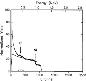
Fig. 5 presents the typical RBS spectrum of the CH4
ySiH s1 sample. The scattered points indicate the4
experimental data and the smooth line represents the simulated fit to the data. The channel numbers, at which steps occur, correspond to those of carbon and silicon. Similar data measured on the other samples deposited at different CH4y SiH4 flow ratios show only small variations from Fig. 5. Table 1 shows the ratio of Cy Si
obtained from XPS and RBS analyses. It was found that both XPS and RBS analyzes show the same results on the composition of deposited films.
According to XTEM, FTIR, XPS and RBS analyses of this study, we observe that at 200 8C and 1200 W, polycrystalline-SiC film can be grown as the CH4y
SiH4 flow ratio is from 1 to 4. Polycrystalline-Si is obtained when the CH4y SiH flow ratio is 0.5. We4
expect that the mixed films of Si and SiC, or SiCX are
possibly grown when the ratio is between 0.5 and 1 because in a previous study w15x, we reported that a mixed film of poly-Si and a-SiC was obtained when the CH4y SiH flow ratio is less than 2, using H as the4 2
carrier gas. Therefore, we believe that the transmission region maybe too narrow to be observed in this study
when Ar is used as the carrier gas. Also, according to FTIR, XPS and RBS analyses, we find that at 200 8C and 1200 W, stoichiometric SiC films can be grown as the CH4y SiH4 flow ratio is as high as 5 and no amorphous carbon is observed. The deposition of amor-phous SiC (a-SiC) is confirmed by the XTEM dark-field and bright-field micrographs with electron diffraction patterns in Fig. 1.
The bonding energy of a Si–H bond is 70.4 kcal moly1, while that for a C–H bond it is 98.8 kcal moly1 w16x. Compared with CH , SiH is easier to
4 4
decompose. This is why the CH4y SiH flow ratio is one4
of the key factors in SiC growth. Deviated from utilizing the high microwave power (1200 W) which supplies
sufficient energy to dissociate CH efficiently and form4
SiC in this work, other experiments in our group which employ a microwave power of 300 W or lower show that no SiC is deposited at all the above CH4y SiH flow4
ratios under similar growth conditions. At the same time, since only poly-crystalline Si films are obtained, it suggests that the sticking coefficient of CH radicalsx
is lower than that of SiH radicals. Therefore, when thex
CH4y SiH flow ratio is 0.5, the amount of adsorbed4
CH radicals is insufficient to react with SiH for SiCx x
formation and consequently the loosely adsorbed CHx
radicals desorb from the surface. The major species adsorbed on substrate surface are SiH radicals so thatx
polycrystalline Si is deposited. As the CH4y SiH flow4
ratio is increased to 1 by increasing CH , i.e. the4
concentration of adsorbed CHx on the substrate is comparable with that of SiH , the adsorbed SiH andx x
CHx radicals react and form polycrystalline b-SiC. However, when the CH4y SiH flow ratio is increased4
to 5 or higher by further increasing CH flow, i.e. in a4
condition that the amount of CH is much higher thanx
that of SiH , the rate of SiC formation becomes so highx
that the SiC molecules on the substrate surface do not have enough time to migrate to suitable sites for crys-talline SiC formation, resulting in the deposition of amorphous SiC.
Experiments with varied microwave powers were conducted at a total pressure of 20 mtorr and a temper-ature of 200 8C. The CH4y SiH flow ratio was kept4
Fig. 6. XTEM dark-field and bright-field micrographs with selected-area electron diffraction patterns of the films grown at 200 8C, CH4ySiH s2, and a microwave power of4 (a) 300, (b) 500, and (c) 1500 W.
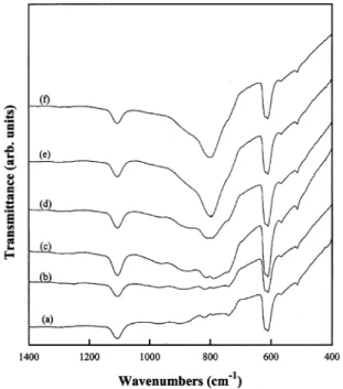
Fig. 7. FTIR transmission spectra of the Si substrate and the films deposited at various microwave powers.(a) Si substrate, (b) 300, (c) 500,(d) 800, (e) 1200, and (f) 1500 W.
different microwave powers were investigated and the results are shown in Fig. 6. When the microwave power is 300 W, Fig. 6a indicates that only polycrystalline Si is deposited. The XTEM micrograph of amorphous SiC is shown in Fig. 6b which is deposited at 500 W. However, when the microwave power is increased to 1200 W and higher, polycrystalline b-SiC films are deposited as shown in Fig. 6c.
Fig. 7 shows FTIR spectra of the bare silicon wafer and the films deposited at different microwave powers. The films grown at 300 W have a characteristic curve identical to that of the bare silicon, indicating that no SiC bonds were formed. An absorption peak at 800 cmy1, due to the stretching mode of SiC, can be found in the other four curves measured from the 500, 800, 1200 and 1500 W samples. The full width at half-maximum(FWHM) of this peak becomes narrower with
increasing microwave power, which indicates that film crystallinity is improved at higher microwave powers. Therefore, a sufficient microwave power is required to deposit polycrystalline b-SiC.
When the microwave power is as low as 300 W, the deposited film is still poly-Si(Fig. 6a) even at a CH y4
SiH flow ratio of 2. That is still because the energy4
needed for SH formation is lower than that of CHx 4
decomposition and the energy is enough for the subse-quent decomposition of SiH to occur. However, at 500x
W microwave power, the energy supplied by plasma may be enough for the dissociation of CH so that most4
SiH radicals can react with CH radicals to form SiC,x x
which may not have enough energy for surface rear-rangement. Therefore, amorphous SiC could be observed in the film (Fig. 6b). As the microwave power is increased to 1200 W and higher, the supplied energy is sufficient for both the formation of radicals and the crystallization of amorphous SiC into polycrystalline b-SiC (Fig. 6c). The FTIR data (Fig. 7) also show the change of film type from poly-Si to SiC.
The self-induced bias voltage observed during the film deposition is between 0 and 10 V and varies within a narrow range. We believe that there should be no significant influence of self-induced bias voltage on the SiC formation due to such a small value of self-induced bias voltage.
4. Conclusion
b-SiC films were deposited on silicon substrates by
ECR-CVD from SiH4y CH y Ar mixtures at 200 8C.4
Crystalline structure and chemical composition of the deposited film were influenced by CH4y SiH flow ratio4
and microwave power. With a sufficient energy supply from microwave power of 1200 W and a CH4y SiH4
flow ratio of 1 and higher, stoichiometric SiC could be deposited on Si substrates. For the case of microwave power 1200 W, polycrystalline b-SiC was grown at
CH4y SiH flow ratios between 1 and 4, whereas amor-4
phous SiC was obtained at the CH4y SiH flow ratios4
higher than 4. Under CH4y SiH flow ratio and temper-4
ature of 2 and 200 8C, respectively, when the CH4y
SiH flow ratio was 0.5, only polycrystalline Si could4
be deposited. When the microwave power was 300 W, polycrystalline Si was deposited. At a microwave power of 500 W, amorphous SiC film was deposited. However, when the microwave power was increased to 1200 W and higher, polycrystalline b-SiC films were deposited.
Acknowledgments
This work was supported by Republic of China National Science Council under Contract No. ‘NSC87-2214-011-011’.
References
w1x M. Bhatnagar, B.J. Baliga, IEEE Trans. Electron Devices 40 (1993) 645.
w2x J.D. Hwang, Y.K. Fang, Y.J. Song, D.N. Yaung, Jpn. J. Appl. Phys. 34(1995) 1447.
w3x H.J. Kim, R.F. Davis, J. Appl. Phys. 60(1986) 2897.
w4x E.G. Wang, Physica B185(1993) 85.
w5x T. Takeuchi, H. Amano, K. Hiramatsu, N. Sawaki, I. Akasaki, J. Cryst. Growth 115(1991) 634.
w6x M. Diani, J.L. Bischoff, L. Kubler, D. Bolmont, Appl. Surf. Sci. 68(1993) 575.
w7x M. Katsuno, T. Futagi, Y. Ohta, H. Mimura, K. Kitamura, Appl. Surf. Sci. 70y71(1993) 675.
w8x K.L. Cheng, H.C. Cheng, C.C. Liu, C. Lee, T.R. Yew, Jpn. J. Appl. Phys. 34(1995) 5527.
w9x C.H. Chen, C.M. Wan, T.R. Yew, Appl. Phys. Lett. 62(1993) 3126.
w10x P.J. Grunthaner, F.J. Grunthaner, R.W. Fathauer, T.L. Lin, M.H. Hecht, L.D. Bell, W.J. Kaiser, Thin Solid Films 183 (1989) 197.
w11x D. Briggs, M.P. Seah, Practical Surface Analysis by Auger and X-ray Photoelectron Spectroscopy, Wiley, New York, 1983. w12x P. Villars, L.D. Calvert, Pearson’s Handbook of
Crystallograph-ic Data for IntermetallCrystallograph-ic Phases, 2, ASM International, Ohio, 1991.
w13x P. Rai-Choudhury, N.P. Formigoni, J. Electrochem. Soc. 116 (1969) 1440.
w14x P.A. Taylor, M. Bozack, W.J. Choyke, J.T. Yates, J. Appl. Phys. 65(1989) 1099.
w15x C.C. Liu, C. Lee, K.L. Cheng, H.C. Cheng, T.R. Yew, J. Electrochem. Soc. 142(1995) 4279.