Herbert Zirath, Senior Member, IEEE, Yun-Chi Wu, Chin-Te Wang, and Ching-Ting Lee, Fellow, IEEE
Abstract—This paper presents the parametric study of RF-via (0-level) and flip-chip bump (1-level) transitions for applications of packaging coplanar RF-MEMS devices. The key parameters were found to be the bumps’ and vias’ positions and the overlap of the metal pads, which should be carefully considered in the entire two levels of packages. The length of the backside transmission line, determining the MEMS substrate area, showed minor influence on the interconnect performance. With the experimental results, the design rules have been developed and established. The optimized interconnect structure for the two levels of packages demonstrates the return loss beyond 15 dB and the insertion loss within 0.6 dB from dc to 60 GHz.
Index Terms—Fabrication, interconnections, microelectrome-chanical devices, microwave technology, packaging.
I. INTRODUCTION
R
ADIO-FREQUENCY micro-electro-mechanical system (RF-MEMS) devices have demonstrated great potential for applications at millimeter-wave frequencies because of sev-eral advantages such as high signal linearity, low insertion loss, and power saving [1]. For RF-MEMS devices to be reliably used, the devices have to be packaged in a stable and hermetic environment [2]. However, the key requirement for packagingManuscript received August 13, 2008; revised February 09, 2009; July 09, 2009. First published December 04, 2009; current version published February 26, 2010. This work was supported in part by the National Science Council under Contract NSC 96-2752-E-009-001-PAE and in part the Ministry of Eco-nomic Affairs, Taiwan, under Contract 95-EC-17-A-05-S1-020. This work was recommended for publication by Associate Editor A. Chiou upon evaluation of the reviewers comments.
L.-H. Hsu and W.-C. Wu are with the Department of Material Science and Engineering, National Chiao Tung University, Hsinchu 300, Taiwan and also with Department of Microtechnology and Nanoscience, Chalmers University of Technology, SE-412 96 Göteborg, Sweden (e-mail: jones2.mse94g@nctu. edu.tw; [email protected]).
E. Y. Chang is with the Department of Materials Science and Engineering, National Chiao Tung University, Hsinchu 300, Taiwan and also with Depart-ment of Electronics Engineering, National Chiao Tung University, Hsinchu 300, Taiwan (e-mail: [email protected]).
H. Zirath is with the Department of Microtechnology and Nanoscience, Chalmers University of Technology, SE-412 96 Göteborg, Sweden (e-mail: [email protected]).
Y.-C. Wu and C.-T. Wang are with the Department of Materials Science and Engineering, National Chiao Tung University, Hsinchu 300, Taiwan (e-mail: [email protected]).
C.-T. Lee is with the Department of Electrical Engineering, National Cheng Kung University, Tainan 701, Taiwan (e-mail: [email protected]).
Color versions of one or more of the figures in this paper are available online at http://ieeexplore.ieee.org.
Digital Object Identifier 10.1109/TADVP.2009.2034137
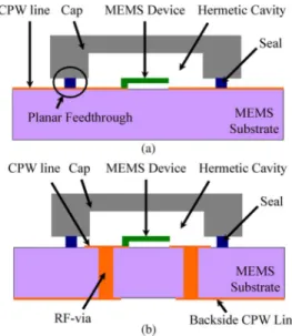
Fig. 1. Two main 0-level interconnect schemes for RF-MEMS devices. (a) RF planar feed-through. (b) RF-Via transition.
is that it should not lead to any performance degradation of RF-MEMS devices, especially the RF characteristics.
At 0-level packaging, a ceramic cap or metal can is usually employed to form a hermetic cavity for sealing the RF-MEMS devices. Fig. 1 shows two main 0-level interconnect schemes for RF-MEMS devices, RF direct feed-through and RF-via transi-tion [1], [2]. RF feed-through scheme requires a thin dielectric layer on the transmission line to pass RF signals through the sealed cap, which causes additional return loss and insertion loss due to the impedance mismatching [3], [4]. Furthermore, the hermeticity of the cavity is not so good since the seals have to cross over the planar transmission line, resulting in degradation of device reliability. The second scheme of the 0-level package is the RF transition by vertical RF-via transitions. A silicon mi-cromachined on-wafer package scheme for RF-MEMS switch was reported using dc and RF vertical via transitions through the wafer [5], [6], which can easily form a real hermetic package for MEMS devices because the hermeticity of the sealing can be achieved by using soldering or gold–gold thermocompression at the seals. However, RF vertical via transitions can have strong impacts on the performances of the packaged RF-MEMS de-vices because of the involved via parasitics. When operating fre-quency increases, a poor consideration in packaging can result in serious reflection and impedance mismatch, causing signal
Fig. 2. Three main possible 0/1-level packaging structures (a) planar RF feedthrough with wire-bonding (b) planar RF feedthrough with flip-chip (c) RF-via transition with bump interconnect (similar to “hot-via”).
loss. The situation becomes worse if the packaging level in-creases further.
At 1-level packaging, there are several possible packaging ar-chitectures depending on which 0-level package used. Fig. 2 il-lustrates three main possible 0/1-level packaging structures. For planar RF feed-through, both wire-bonding and flip-chip can be used as the 1-level interconnect. Wire-bonding [Fig. 2(a)] uses attenuated wires to connect 0- and 1-level packages, which generates serious parasitic effects at higher frequency due to its long interconnect length. Flip-chip, on the other hand, is a more promising high frequency interconnect technology be-cause of excellent RF performance [7], high input/output (I/O) density, fast assembly speed and higher production yield. From Fig. 2(b), however, when using planar feed-through, higher flip-chip bump height and additional flip-chip area for pads are needed. It increases the package cost and the size is not compact enough. For RF-via interconnect as shown in Fig. 2(c), a face-up bump transition architecture similar to “hot-via” [8]–[10] can be used to realize a compact and high performance package. Since it is a face-up mounting technology, the chip can be optically in-spected after bonding and the detuning effect can also be effec-tively reduced [8]–[10].
From literature, most researches related to RF-MEMS de-vice packaging are mainly focused on 0-level package. Very few studies pay attention on 1-level package. In our previous report, we have presented an optimized 0/1-level RF-via interconnect structure with good performance up to 60 GHz [11]. To further establish the design concepts for coplanar RF-MEMS devices packaging, the 0/1-level interconnect structures using RF-via and bump transitions are experimentally investigated. The in-terconnect structures with various designed key parameters have been fabricated and characterized from dc to 67 GHz. Based on the experimental results, the optimized interconnect structure including two levels of packages demonstrates the return loss less than 15 dB and the insertion loss within 0.6 dB from dc to 60 GHz, showing the feasibility for application of such tech-nology for the coplanar RF-MEMS device packaging.
II. DESIGNPARAMETERS
Fig. 3 illustrates the schematic of the 0/1-level interconnect structure studied in this paper where the RF-via interconnect is used in 0-level and the vertical bump transition is used in 1-level. The sealing cap is not realized in this study. For the demon-strated interconnect structures, the material of the MEMS sub-strate and motherboard were GaAs and ; the thickness of the MEMS substrate and motherboard were 50 and 254 , respectively. The conductor metal was 3 Au. The character-istic impedances of the coplanar waveguide (CPW) trans-mission lines on the MEMS substrate and motherboard were both equal to 50 . The total length of the back-to-back 0/1-level RF-via interconnect structure was 3000 , including 1500 on the MEMS substrate and 1500 on the motherboard.
In the design, a finite-ground coplanar (FGC) waveguide was employed instead of the conventional CPW with large ground planes to effectively suppress the parallel plate and higher-order modes. To eliminate coupling of CPW mode into slotline mode, the symmetry was always kept along the signal transmission lines [12]. From the literatures, the smaller diameter and larger height of the bumps and vias contribute to an inductive effect, therefore giving compensation to the capacitive part in the ver-tical transitions, [13]. Considering the process uniformity in the experiments, the diameters of the bump and via were fixed to 50 and the bump height was 30 . The physical dimen-sions and key parameters are summarized in Fig. 4. The param-eters in investigation are the distances between ground bumps and vias ( and ), the metal overlaps ( and ), and CPW length and width on the backside of the MEMS substrate
Fig. 4. Illustrations of the designed physical dimensions and key parameters (a) top-view (b) cross section and (c) list of physical dimensions and key pa-rameters.
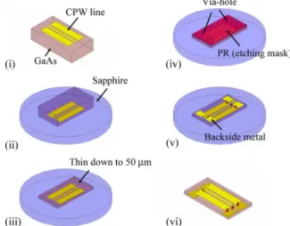
Fig. 5. The process flow of the RF-via interconnect structure.
( and ). The interconnect structures with variable param-eters were experimentally fabricated and RF characterized to evaluate the best parameters for packaging RF-MEMS devices through 0/1-level packages.
III. PACKAGEFABRICATION
The demonstrated RF-via interconnect structure was fabri-cated house. Fig. 5 shows the process flow of the RF-via in-terconnect structure. The CPW transmission lines were first pat-terned on the front side of the GaAs MEMS substrate by pho-tolithography and electroplating process. The GaAs substrate was then mounted on a sapphire carrier and thinned down to 50 . RF-via etching was performed by using inductively cou-pled plasma (ICP) etcher with and gas mixture, where the etching conditions such as the gases mixture ratio, pressure, and etching power were optimized to achieve high etching rate, high etching selectivity, and good etching profiles. Fig. 6 shows the cross-sectional SEM image of the etched via-hole. The back-side metal was patterned on the backback-side of the MEMS sub-strate. The demounting process was to immerse the fabricated
Fig. 6. Cross-sectional SEM image of the etched via-hole.
Fig. 7. The process flow of theAl O motherboard.
interconnect structure into the stripping solution to remove the sapphire carrier.
The motherboard with Au CPW circuits and bumps were fabricated by standard Au bumping process of CSDlab, NCTU [14]. Fig. 7 illustrates the process flow step by step. In the beginning, the metal seed layers Ti and Au are deposited onto the motherboard. Then, the thin photoresists are patterned to electroplate the Au CPW transmission line. After the electroplating of the transmission line, the thin photoresists are removed. The thick photoresists are patterned. After that, the pillar bumps are electroplated and the seed layers are removed. The SEM image of the fabricated motherboard with Au pillar bumps is shown in Fig. 8.
Finally, the fabricated MEMS substrate with RF-via and the motherboard with Au bumps were assem-bled together by Au-to-Au thermo-compression process to complete the final interconnect structure. The bonding parameters are: bonding force g (for six bumps), bonding temperature (for both sides) and bonding hold time s. Fig. 9 shows the SEM image of the fabricated 0/1-level RF-via interconnect structure.
IV. EXPERIMENTALRESULTS ANDDISCUSSIONS
The scattering parameters of the fabricated 0/1-level RF-via interconnect structures were characterized to 67 GHz using
Fig. 8. SEM image of the fabricated Au bumps onAl O motherboard.
Fig. 9. SEM image of the fabricated back-to-back 0/1-level RF-via intercon-nect structure.
Fig. 10. Measured S-parameters of the interconnect structures with different distances between ground bumps(W ).
on-wafer probing measurement system with an Agilent precision network analyzer (PNA) E8361A. During the mea-surements, a 10-mm-thick layer of Rohacell 31 (
at 26.5 GHz) was placed between the samples and the metal chuck of the probe station to avoid the grounded backside under the substrates. For the interconnect structure, three groups of parameters, i.e., bump and via-hole positions, metal pad over-laps, and backside CPW dimensions were investigated. To validate the measured results, 3-D electromagmetic (EM) field simulation was performed with CST (Computer Simulation Technology) Microwave Studio on the same structures.
distances between ground vias(W ).
Fig. 12. Simulated S-parameters of the interconnect structures with different distances between ground bumps(W ).
A. Bump and Via-Hole Positions
Figs. 10 and 11 show the measured results of the intercon-nect structures with different distances between ground bumps and vias ( and ). From the measured results, as the dis-tances between bumps and vias changed from 216 to 296 , the return losses were improved about 8 dB for the case of and about 5 dB for the case of at 40 GHz, which can be interpreted by the internal compensation effect at the transitions [13]. However, when the distance was further increased to 376 , the reflection became worse. From the simulation results shown in Figs. 12 and 13, the trends are similar. The structures with and
have the best performances. It shows that there is an optimum in-ternal compensation in the 0/1-level RF-via interconnects. Thus, to achieve the best counterbalance of the parasitic effects, the lo-cations of the ground bumps and vias should be well-arranged in the proper positions to obtain the lowest reflection.
B. Metal Pad Overlaps
To improve the transmission characteristics, it is effective to reduce the induced capacitance by decreasing the metal pad overlap areas [13]. From the measured results in Figs. 14 and 15, when the metal pad overlaps ( and ) decreased from 160 to 80 , the measured return loss improved about 8 dB (for ) and 6 dB (for ) at 40 GHz. Figs. 16 and 17 show the simulation results of the corresponding interconnect structures. As can be seen from both the measured and simulated results,
Fig. 13. Simulated S-parameters of the interconnect structures with different distances between ground vias(W ).
Fig. 14. Measured S-parameters of the interconnect structures with different bump pad overlap(l ).
Fig. 15. Measured S-parameters of the interconnect structures with different via-hole pad overlap(l ).
the reflections were effectively improved by reducing the bump and via pad overlap due to less parasitic capacitance involved. Therefore, the metal overlaps should be kept as small as pos-sible to lower reflection at the transitions.
C. Backside CPW Dimensions
The CPW length on the backside of the MEMS substrate determines the RF-MEMS device area, which effects the final cost of the RF-MEMS devices. Shorter backside CPW length saves MEMS substrate area. As can been seen from the measured results in Fig. 18 (thick lines), when the length was increased from 80 to 150 , the measured return loss in-creased about 2 dB at 40 GHz, showing minor influence on the
Fig. 16. Simulated S-parameters of the interconnect structures with different bump pad overlap(l ).
Fig. 17. Simulated S-parameters of the interconnect structures with different via-hole pad overlap(l ).
interconnect performance. Furthermore, the simulation results (thin lines) revealed similar trend with the measured results, in-dicating the backside CPW length should be kept as short as possible, which would save the MEMS substrate area without causing any degradation of the interconnect performance. For the width of the backside CPW , similar phenomenon was observed. From Fig. 19, when the width was increased from 80 to 240 , the return loss remained almost the same for both the measurement and simulation results.
V. OPTIMIZATION
The 0/1-level RF-via interconnect structure was then opti-mized based on the experimental results shown above. Fig. 20 shows the measured and simulated results of the back-to-back interconnect structure with the optimized parameters, i.e.,
, , , and
. From the measured results, the return loss was less than 30 dB from dc to 20 GHz; from 20 to 60 GHz, the return loss was less than 15 dB. The insertion loss was within 0.6 dB from dc to 60 GHz, showing good wideband intercon-nect performance up to 60 GHz. The simulation results agree well below 40 GHz. Beyond 40 GHz, the simulated return loss is a little higher compared with the measured return loss due to the shift of the resonance frequency at higher frequencies. The
Fig. 18. Measured and simulated S-parameters of the interconnect structures with different backside CPW lengths(l ).
Fig. 19. Measured and simulated S-parameters of the interconnect structures with different backside CPW widths(w ).
simulated insertion loss, as a result, is higher than the measured insertion loss. Besides, the loss tangent of the dielec-tric materials (GaAs and ) and the resistivity of the metal (Gold) in the simulation models were set to be frequency in-dependent. In reality, however, these material properties would vary with the frequency. In summary, these could be the reasons why the simulated insertion loss does not match well with the measured results after 40 GHz.
VI. CONCLUSION
For coplanar RF-MEMS devices packaging, the design guideline of 0/1-level RF-via interconnect are determined from
Fig. 20. Measured and simulated S-parameters of the optimized 0/1-level RF-via interconnect structure.
the experimental results. First, to give the effective inter-com-pensation and to achieve low reflection at the interconnect, position of the ground bumps and vias should be considered. Second, the smaller overlap of the metal pads gives lower reflection at the interconnect due to the reduction of the induced capacitance. Third, the backside area for signal transmission from 0- to 1-level must be kept as small as possible to save the MEMS substrate area due to its minor influence on the device performance based on the experimental results. The 0/1-level RF-via interconnect structure with optimized key parameters demonstrated wideband interconnect performance from dc to 60 GHz with return loss less than 15 dB and insertion loss within 0.6 dB, showing the feasibility of such technology for RF-MEMS packaging applications up to V-band.
ACKNOWLEDGMENT
The authors would like to thank C. H. Huang and Y. C. Hu for the help of the experimental work.
REFERENCES
[1] G. M. Rebeiz and J. B. Muldavin, “RF MEMS switches and switch circuits,” IEEE Microwave Mag., vol. 2, no. 4, pp. 59–71, Dec. 2001. [2] H. J. De Los Santos, G. Fischer, H. A. C. Tilmans, and J. T. M. van
Beek, “RF MEMS for ubiquitous wireless connectivity. Part II. Appli-cation,” IEEE Microwave Mag., vol. 5, no. 4, pp. 50–65, Dec. 2004. [3] A. Jourdain, X. Rottenberg, G. Carchon, and H. A. C. Tilmans,
“Opti-mization of 0-level packaging for RF-MEMS devices,” in Proc.
Trans-ducer’03, Boston, MA, Jun. 2003, vol. 2, pp. 1915–1918.
[4] G. Carchon, A. Jourdain, O. Vendier, J. Schoebel, and H. A. C. Tilmans, “Integration of 0/1-level packaged RF-MEMS devices on MCM-D at millimeter-wave frequencies,” in Proc. Electron. Compon.
Technol. Conf., Jun. 2005, vol. 2, pp. 1664–1669.
[5] A. Margomenos, D. Peroulis, J. P. Becker, and L. P. B. Katehi, “Sil-icon micromachined interconnects for on-wafer packaging of MEMS devices,” in Silicon Monolithic Integrated Circuits RF Syst., Sep. 2001, pp. 33–36.
[6] A. Margomenos, D. Peroulis, K. J. Herrick, and L. P. B. Katehi, “Sil-icon micromachined packages for RF MEMS switches,” in Eur.
Mi-crow. Conf., Oct. 2001, pp. 1–4.
[7] D. Staiculescu, J. Laskar, and E. M. Tentzeris, “Design rule devel-opment for microwave flip-chip applications,” IEEE Trans. Microw.
Theory Tech., vol. 48, no. 9, pp. 1476–1481, Sep. 2000.
[8] F. J. Schmuckle, A. Jentzsch, C. Gassler, P. Marschall, D. Geiger, and E. Heinrich, “40 GHz hot-via flip-chip interconnects,” in IEEE MTT-S
Int. Microwave Symp. Dig., Jun. 2003, vol. 2, pp. 1167–1170.
[9] A. Bessemoulin, C. Gaessler, P. Marschall, and P. Quentin, “A chip-scale packaged amplifier MMIC using broadband hot-via transitions,” in Eur. Microw. Conf., Oct. 2003, pp. 289–292.
[13] A. Jentzsch and W. Heinrich, “Theory and measurements of flip-chip interconnects for frequencies up to 100 GHz,” IEEE Trans. Microw.
Theory Tech., vol. 49, no. 5, pp. 871–878, May 2001.
[14] W. C. Wu, H. T. Hsu, E. Y. Chang, C. S. Lee, C. H. Huang, Y. C. Hu, L. H. Hsu, and Y. C. Lien, “Flip-chip packaged In0.52Al0.48As/ InGaAs metamorphic HEMT device for millimeter wave application,” in Proc. CS-MAX, Compound Semicond. Manufact. Expo, Nov. 2005, pp. 94–97.
Li-Han Hsu (S’07) was born in Tainan, Taiwan, in
1981. He received the B.S. and M.S. degrees from the Department of Materials Science and Engineering. National Chiao Tung University, Hsinchu, Taiwan, in 2003 and 2005, respectively. He is currently working toward the dual Ph.D. degrees in Department of Materials Science and Engineering, National Chiao Tung University, Hsinchu, Taiwan and Depart-ment of Microtechnology and Nanoscience, MC2, Chalmers University of Technology, Göteborg, Sweden.
His main research interest is millimeter-wave packaging technology including flip-chip interconnect, hot-via interconnect, and integration of V-/E-band MCM transceiver modules.
Wei-Cheng Wu was born in Hsinchu, Taiwan, in
1979. He received the B.S. degree and the Ph.D. degree from Materials Science and Engineering De-partment, National Chiao Tung University, Hsinchu, Taiwan, in 2001 and 2008, respectively.
He is currently working as a Research Engineer at Taiwan Semiconductor Manufacturing Company Ltd. His research interests include fabrication, characterization, and packaging technologies of compound semiconductor devices, RF-MEMS, and ICs for high-frequency applications, especially flip chip interconnect and various transitions design.
Edward Yi Chang (S’85–M’85–SM’04) received
the B.S. degree in materials science and engineering from the National Tsing Hua University, Hsinchu, Taiwan, in 1977 and the Ph.D. degree in materials science and engineering from the University of Minnesota, MN, in 1985.
He was with the Unisys Corporation GaAs Component Group, Eagan, MN, from 1985 to 1988 and with the Comsat Labs Microelectronic Group from 1988 to 1992. He worked on the GaAs MMIC programs on both groups. He was with the National Chiao Tung University (NCTU), Hsinchu, in 1992. In 1994, he helped set up the first GaAs MMIC production line in Taiwan and became the President of Hexawave Inc., Hsinchu, in 1995. In 1999, he returned to NCTU with a teaching position, where he is currently the Head and Professor of the Department of Materials Science and Engineering. His research interests include new device and process technologies for compound semiconductor RFICs for wireless communication.
Dr. Chang is a Distinguished Lecturer of the IEEE Electronic Device Society.
quency semiconductor devices and circuits. His main research interests include InP-HEMT devices and circuits, SiC and GaN-based transistors for high-power applications, device modeling including noise and large-signal models for FET and bipolar devices, and foundry-related monolithic microwave ICs for millimeter-wave applications based on both III-V and silicon devices. He is also working part-time at Ericsson AB, Mölndal, Sweden, as a Microwave Circuit Expert. He has authored or coauthored more than 220 papers in international journals and conference proceedings and one book, and he holds four patents.
Yun-Chi Wu was born in Chiayi, Taiwan. He
received the B.S. degree from Materials Science and Engineering Department, Tatung University, Taipei, Taiwan, in 2001, the M.S. degree in materials science and engineering, in 2003, from National Chiao Tung University, Hsinchu, Taiwan, where he is currently working toward the Ph.D. degree in CSDLab., Materials Science and Engineering Department.
His research is focused on HEMT device and process technologies for wireless communication applications.
Chin-Te Wang was born on November 6, 1983
in Taipei, Taiwan. He received the B.S. degree in Department of Materials Science and Engineering from National Chung Hsing University (NCHU), Taichung, Taiwan, in 2006.
He was interested in electric materials when he studied in NCHU. He joined the Compound Semiconductor Device Laboratory in National Chiao Tung University (NCTU) and started his M.S. and Ph.D. degree in 2006.
Ching-Ting Lee (F’09) was born in Taoyuan,
Taiwan, Republic of China, on November 1, 1949. He received the B.S. and M.S. degrees from the Electrical Engineering Department, the National Cheng Kung University, Taiwan, in 1972 and 1974, respectively, and the Ph.D. degree from the Elec-trical Engineering Department, Carnegie-Mellon University, Pittsburgh, PA, in 1982.
He worked on Chung Shan Institute of Science and Technology, before he joined the Institute of Optical Sciences, National Central University, Chung-Li, Taiwan, as a Professor in 1990. He works on National Cheng Kung University as the Dean of the College of Electrical Engineering and Computer Science and the Professor of the Institute of Microelectronics, Department of Electrical Engineering in 2003. He is the distinguished research professor of National Cheng Kung University. His current research interests include nano materials and devices, light emission of Si nanoclusters, nanostructure of solar cells, GaN-based light-emitting diodes and lasers, GaN-based field effect transistors. His research activities have also involved in the research concerning III-V semiconductor lasers, photodetectors and high-speed electronic devices, and their associated integration for electrooptical integrated circuits.
Dr. Lee has received the outstanding Research Professor Fellowship from the National Science Council (NSC), Republic of China, distinguish service award from Institute of Electrical Engineering Society, the Optical Engineering Medal from Optical Engineering Society and Distinguish Electrical Engineering pro-fessor award from Chinese Institute of Electrical Engineering Society.