應用於超寬頻系統之可調頻低雜訊放大器
72
0
0
全文
(2) 應用於超寬頻系統之可調頻低雜訊放大器設計. Broadband Tunable Low Noise Amplifier for Ultra-Wideband System. 研 究 生:陳仰鵑. Student:Yang-Chaun Chen. 指導教授:郭建男. Advisor:Chien-Nan Kuo. 國 立 交 通 大 學 電子工程學系 電子研究所碩士班 碩 士 論 文 A Thesis Submitted to Department of Electronics Engineering & Institute of Electronics College of Electrical Engineering and Computer Science National Chiao Tung University In Partial Fulfillment of the Requirements For the Degree of Master In Electronic Engineering July 2005 Hsinchu, Taiwan, Republic of China. 中 華 民 國 九十四 年 七 月.
(3) 應用於超寬頻系統之可調頻低雜訊放大器設計. 學生 : 陳 仰 鵑. 指導教授 : 郭 建 男 教授. 國立交通大學 電子工程學系 電子研究所碩士班 摘要 本篇論文主要是利用標準 0.18µm CMOS 製程設計應用於超寬頻系統前端接 收器之可調頻低雜訊放大器。第一顆晶片,設計適用於接收端超寬頻系統之可調 頻率放大器被設計與分析,利用柴比雪夫濾波器設計達到寬頻之輸入阻抗匹配, 利用電晶體可變電容來調變頻率。量測結果顯示可調變頻率範圍縮小,且操作頻 率往低頻移動,可調頻率為 5.1GHz 到 6.8GHz 有最高功率增益(S21) 7.4dB,以 及最低雜訊指數 5.7dB,消耗之功率為 19.51mW。依據第一顆晶片量測結果,經 過驗證反察,發現可變電容的容值比預期大且可調變範圍比預期小,原因出在模 擬的可變電容模組和所佈局的模組不同而產生,因此,第二顆晶片修正可變電容 模組,且加上切換 MIM 電容,增加可調頻率範圍;並改用諧振匹配原理達到輸入 寬頻阻抗匹配,降低雜訊指數和功率消耗,修正晶片量測結果顯示,可調頻率為 6.3GHz 到 9.4GHz,最高增益 9.3dB,發生在 9.4GHz,平均雜訊指數為 4.5dB, 消耗功率為 17.44mW。接著為了達到 3GHz 到 8GHz 之超寬頻可調頻率,考慮可變 電容之可調範圍的先天限制,因此,第三顆晶片結合 MEMS 電感的高 Q 特性,設. i.
(4) 計切換電感負載,達到更寬頻之調頻設計。比較前兩顆切換 MIM 電容和第三顆切 換 MEMS 電感的 LNA 設計,MEMS 高 Q 特性的優勢,明顯使電路達到高增益且超寬 可調頻率,及低雜訊,低功率的設計目的。. ii.
(5) Broadband Tunable Low Noise Amplifier for Ultra-Wideband System. Student: Yang-Chuan Chen. Advisor: Prof. Chien-Nan Kuo. Department of Electronics Engineering & Institute of Electronics National Chiao-Tung University. ABSTRACT The objective of this thesis is aimed at design of low noise amplifier (LNA) with tunable output frequency for the ultra-wideband (UWB) receiver system using standard 0.18um CMOS process. Three LNA circuits have been implemented. In the first chip, a wideband tunable low noise amplifier is analyzed and designed using the Chebyshev filter design to achieve broadband input impedance matching and a MOS varactor provides frequency tuning capability. The measured data show that the tunable frequency range is from 5.1GHz to 6.8GHz, narrower and lower as compared to the designed values. The frequency drift is due to the inconsistency of the varactor models in the circuit simulator and the circuit layout. Therefore, the second chip is designed to revise the tunable mechanism. The measurement data of the second chip shows that the frequency tunable range is 6.3GHz to 9.3GHz. To extend the tunable frequency range to 3GHz to 8GHz and still maintain the high power gain is limited by the poor quality factor of the large MIM capacitor value. iii.
(6) Therefore, the high Q micromachined inductors are integrated with the third chip to achieve the wideband tunable range and good noise performance. Furthermore, power consumption is reduced by an external capacitor placed across the gate and the source ports of the input transistor.. iv.
(7) 誌謝 論文得以順利完成,首要感謝我的指導教授郭建男博士這兩年來的照顧與 指導,使我對射頻積體電路設計有更深層的認知,更學得嚴謹的研究態度。感謝 不吝指導的博班學長昶綜和均琳;已畢業的學長們,建嘉,敬銘,柏之,上逸, 英瑞,志修,宏達,碩一的懵懂期多虧有你們的協助;互相鼓勵,一起研究,一 起成長,度過這兩年的維嘉,坤宏,政偉;一起討論分享的學弟,子倫,達道, 岱原,杰利,冠華;因為有了大家,實驗室就像個溫馨的家,這兩年來,非常感 謝大家的照顧。感謝陳巍仁和鄭裕庭教授,兩年來在計畫的會議上所給予的指 導,得以讓我的論文更加完整。還要感謝國家晶片中心(CIC)在電路下線實做和 晶片量測上所提供的協助。 最後,要特別感謝父母的栽培與鼓勵,及所有家人的支持,男友振的陪伴, 朋友的打氣,讓我快樂度過碩士生涯,還有其他要感謝的人,在此一併謝過。. 陳仰鵑 九十四年 七月. v.
(8) CONTENTS ABSTRACT (CHINESE) ...............................................i ABSTRACT (ENGLISH) ............................................ iii ACKNOWLEDGEMENT.............................................v CONTENTS...................................................................vi. TABLE CAPTIONS ..........................................ix FIGURE CAPTIONS ........................................x Chapter 1. Introduction...............................................1. 1.1 Ultra-Wideband Communication System................ 1 1.2. Motivation .................................................................. 2. 1.3 Thesis Organization................................................. 32. Chapter 2. The Fundamentals in LNA Design ..........4. 2.1. Noise in MOSFET................................................... 4. 2.2. Low Noise Amplifier Basic .................................... 7 2.2.1 Low Noise Amplifier Topology and Basic .............................7 2.2.2 Inductive Source Degeneration LNA Analysis .....................9. Chapter 3. Ultra-Wideband Tunable Low Noise Amplifier.................................................12. 3.1 Introduction.............................................................. 12 3.2 A 6 to 10GHz UWB Tunable LNA.......................... 12 3.2.1 Ultra-wideband Tunable LNA Circuit Topology ...............12 vi.
(9) 3.2.2 Broadband matching Techniques ..........................................13 3.2.3. Tunable RLC Tank ..................................................................19. 3.2.4 Gain Compensation Technique ..............................................22 3.2.5 Design Considerations and Trade Off .................................23 3.2.6. Consideration of layout ...........................................................24. 3.2.7 Microphotograph of Chip........................................................25 3.2.8 Simulation and Measurement results and Discussion......25. 3.3 Improved 6 to 10GHz UWB Tunable LNA............ 32 3.3.1 Frequency Tunable Mechanism .............................................33 3.3.2 Resonance Matching Technique ............................................35 3.3.3 Design Considerations and Trade Off .................................36 3.3.4. Consideration of layout ...........................................................37. 3.3.5 Microphotograph of Chip........................................................38 3.3.6 Simulaiton and Measurement results and Discussion......38. 3.4 A Tunable LNA with MEMS Inductors for UWB Mode-2 Device ......................................................... 45 3.4.1 Motivation ...................................................................................45 3.4.2. Circuit Architecture ..................................................................45. 3.4.3 MEMs Inductors ........................................................................47 3.4.4 Ultra Wide-band Tunable Load ...........................................48 3.4.5. Noise Considerations .............................................................50. 3.4.6. Consideration of layout ...........................................................52. 3.4.7 Package integreted technique ..............................................54 3.4.8 Simualtion results and comparison.......................................55. Chapter 4 Conclusion ..................................................56 Chapter 5 Future Works .............................................56 vii.
(10) REFERENCES.............................................................57 VITA ............................................................................58 PUBLICATION............................................................58. viii.
(11) TABLE CAPTIONS TABLE 3.1. Element values for Chebyshev Low Pass Filter prototypes…………..16. TABLE 3.2. Summary of measured performance and comparison to other tunable amplifier……………………………………………………………...31. TABLE 3.3. Summary of measured performance and comparison to the previous tunable amplifier..................................................................................44. TABLE 3.4. Summary of simulation performance and comparison to the circuit of section 3.2……………………………………………………….......55. ix.
(12) FIGURE CAPTIONS Fig. 1.1. Multiband spectrum allocation....................................................................2. Fig. 2.1. Common LNA architectures....……...….....................................................7. Fig. 2.2. Cascode LNA architecture....……………………...……………..….….....9. Fig. 2.3. Small-signal model for LNA noise calculations……………………..…..10. Fig. 3.1. Shematic of the poposed ultra-wideband tunable LNA………………….13. Fig. 3.2. The process of filter design……………………………...……………….14. Fig. 3.3. Ladder circuit for low-pass filter prototypes and their element definitions.15. Fig. 3.4. Components convert from low pass filter to bandpass filter ……....……..17. Fig. 3.5. The transformation circuit of low pass filter converted to bandpass filter..17. Fig. 3.6. The small signal model of the input impedance…………………………..18. Fig. 3.7 The first order RLC tank………………………………..……….…..……19 Fig. 3.8 Fix C and tuning L..…………………………………………..……...…….20 Fig. 3.9 Fix L and tuning C……………………………………………..…....…….21 Fig. 3.10 The LC tank transformation………………………………..……….….….22 Fig. 3.11 The small signal model of the input stage………………………..………..22 Fig. 3.12 The quality factor of the inductor Ld ……………………………………….24 Fig. 3.13 Microphotograph of the tunable LNA…………...…………...…….……...25 Fig. 3.14 S21 simulation and measured result of the tunable LNA…………..……...27 Fig. 3.15 The tuning voltage relative to the varactor capacitance……………………27 Fig. 3.16 The tuning voltage relative to the center frequency………………………..28 Fig. 3.17 S11 simulation and measured result of the tunable LNA…….……………28 Fig. 3.18 S22 simulation and measured result of the tunable LNA…………….……29 Fig. 3.19 Noise Figure simulation result……………………………………………..30. x.
(13) Fig. 3.20 IIP3 versus frequency simulation and measured result……………………30 Fig. 3.21 The amended UWB tunable LNA schematic……………………………..33 Fig. 3.22 The tunable mechanism…………………….………………….………….34 Fig. 3.23 The input impedance small signal model………….……….……………..36 Fig. 3.24 The impedance trend in smith chart……………………………..…….…..36 Fig. 3.25 Microphotograph of the amended tunable LNA…………………….…….38. Fig. 3.26 S21 simulation and measured result of the amended tunable LNA….……40 Fig. 3.27 S11 simulation and measured result of the amended tunable LNA….……41 Fig. 3.28 S22 simulation and measured result of the amended tunable LNA…….….42 Fig. 3.29 Noise Figure of the amended tunable LNA…………………………….…..43 Fig. 3.30 IIP3…………...……………………………………………………………..44 Fig. 3.31 The schematic of the tunable LNA for 3~8 GHz………………….….…….46 Fig. 3.32 The suspended inductor with the cross membrane supporting…….……….47 Fig. 3.33 The cross view of the cross membrane inductor……………..…………….48. Fig. 3.34 The measurement result of the cross membrane inductor…………….……48 Fig. 3.35 The tunable mechanism…………………………………………..………..49 Fig. 3.36 The effected inductor………………………………………………………49. Fig. 3.37 The equivalent inductor value…………….………………..………………50. Fig. 3.38 The noise model……………………………………………………………51. Fig. 3.39 Schematic of the tunable LNA fabricated on the chip die………………….52 Fig. 3.40 Layout of the chip die……………………………………………..……….53 Fig. 3.41 Layout of the complete integrated circuit………………………………….54 Fig. 3.42 The bonding technique……………………………………………………..55. xi.
(14)
(15) Chapter 1 Introduction 1.1 Ultra-Wideband Communication System The ultra-wideband (UWB) system is an emerging high-speed and low-power wireless communication approved by Federal Communication Commission (FCC) in 2002 for commercial applications in the frequency range from 3.1- to 10.6-GHz. The IEEE 802.15.3a task group (also called “TG3a”) is developing an UWB standard. Two primary contenders been left after July 2003 meeting are the OFDM-based multiband approach and the dual-band Impulse Radio spread spectrum approach. The multibanded UWB has greater flexibility in coexisting with other international wireless systems and future government regulators, and could avoid transmitting in already occupied bands. The UWB frequency band from 3.1 to 10.6 GHz of the multiband-OFDM access method is divided into several smaller bands. Each of these bands must have a bandwidth greater than 500 MHz to obey the FCC definition of UWB and each band uses frequency hopping to facilitate multiples access [1, 2]. The division of the UWB frequency spectrum into sub-bands is illustrated in Fig. 1.1.The frequency operation for Mode 1 device allocates in 3.1GHz to 5GHz and the one for Mode 2 device allots to 3.1-8GHz. GROUP B. GROUP A. GROUP C. GROUP D. Band #1. Band #2. Band #3. Band #4. Band #5. Band #6. Band #7. Band #8. Band #9. Band #10. Band #11. Band #12. Band #13. 3432 MHz. 3960 MHz. 4488 MHz. 5016 MHz. 5808 MHz. 6336 MHz. 6864 MHz. 7392 MHz. 7920 MHz. 8448 MHz. 8976 MHz. 9504 MHz. 10032 MHz. Fig. 1.1. Multiband spectrum allocation.. 1. f.
(16) 1.2. Motivation As introduced in Section 1.1, UWB is becoming more attractive for low cost. consumer communication applications and that allows overlying existing narrowband systems to result in a much more efficient use of the available spectrum. Thus, UWB is developed to provide a specification for a low complexity, low cost, low power consumption, and high data rate wireless connectivity among devices within or entering the personal operating space and also addressed the quality of service capabilities required to support multimedia data types. One of the proposed leading standards for UWB spectrum allocation is a multi-band with frequency hopping. Nevertheless, the robust multipath tolerance needs to combat inter-carrier interference and tight linear constraint. To relax the linearity limitation of the next stage, the low noise amplifier in the receiver path of the UWB frequency hopping system followed with a frequency tunable load is proposed to reject the out of band interference and to increase the dynamic range. To design a wideband LNA followed by tunable load providing flatness gain over several GHz is a critical challenge for design. In this thesis, we emphasize on the minimum noise figure, gain flatness and ultra-wideband tunable range of the low noise amplifier at low power level.. 2.
(17) 1.3 Thesis Organization This thesis discusses about the tunable LNA design and implementation for the UWB frequency hopping system. In Chapter 2, fundamentals of conventional low noise amplifiers will be introduced. And theoretical MOSFET noise model and noise theory are presented. In Chapter 3, an ultra-wideband tunable LNA is presented in section 3.2, and in section 3.3 the amended circuit is proposed to enhance the tunable range, and then the tunable LNA integrated with high Q MEMS inductors is discussed in section 3.4. In Chapter 4, to conclude the tunable LNA design. In Chapter 5, the future work is described. Some issues that should be noted for future works on this topic are also summarize.. 3.
(18) Chapter 2 The Fundamentals in LNA Design Fundamentals of the low noise amplifier will be introduced. In section 2.1 illustrates the noise sources in MOSFET [3, 4]. The design basic of the low noise amplifier is discussed in section 2.2 [3, 4].. 2.1 Noise in MOSFET The noise performance of LNA is the first consideration because it represents a lower limit to the signal amplified by a circuit without significant deterioration in signal quality. The various sources of electronic noise are considered, and MOSFET’s noise model will be described here. The noise process of thermal noise is random, and we would expect a dependence on the absolute temperature, T. It turns out that thermal noise power is exactly proportional to T. The every physical resistor has a noise source associated with thermal noise. The thermal noise can be represented by v 2 = 4kTR∆f or i 2 = 4kT (1/ R )∆f , where k is Boltzmann’s constant and ∆f is the noise bandwidth in. hertz. Since MOSFETs are essentially voltage-controlled resistors, they exhibit thermal noise. Thus, detailed theoretical considerations lead to the following expression for the drain current noise of FETs: id2 =4kTγ gd0∆f ,. (2-1). where gd0 is the drain-source conductance at zero VDS. The parameter γ has a value of unity at zero VDS and, in long devices, decreases toward a value of 2/3 in saturation. 4.
(19) Note that the drain current noise at zero VDS is precisely that of an ordinary conductance of value gd0. Unfortunately, γ is greater then 2/3 for short channel device, and thus the value will lead to worsen the noise performance as the technology proceeds. Gate noise, ig 2 is another kind of thermal noise due to the thermal agitation of channel charge. The fluctuating channel potential couples capacitively into the gate terminal, leading to a noisy gate current. Although this noise is negligible at low frequencies, it can dominate at radio frequencies. The gate current noise may be expressed as ig2 =4kTδ gg∆f , where gg=. ω 2Cgs2 5gd0. (2-2). .. And δis the coefficient of gate noise, classically equal to 4/3 for long-channel devices while 4 to 6 in short channel one. The gate noise is partially correlated with the drain noise, with a correlation coefficient expressed as. c≡. ig id* id2 ig2. ≈ −0.395 j .. (2-3). The value of -0.395j is exact for long-channel devices. The correlation can be treated by expressing the gate noise as the sum of two components, the first of which is fully correlated with the drain noise, and the second of which is uncorrelated with the drain noise. Hence, the gate noise is re-expressed as ig2 =4kTδ gg(1-|c|2 )+4kTδ gg|c|2 . ∆f. (2-4). Because of the correlation, special attention must be paid to the reference polarity of the correlated component. 5.
(20) Charge trapping leads to the flicker noise, which is a type of noise found in all active devices. These traps capture and release carriers in a random fashion and the time constants associated with the process give rise to a noise signal with energy concentrated at low frequencies. In electronic devices, 1/f noise (flicker noise) arises from a number of different mechanisms, and is most prominent in devices that are sensitive to surface phenomena. Charge trapping phenomena are usually invoked to explain 1/f noise in transistors. Some types of defects and certain impurities can randomly trap and release charge. The trapping times are distributed in a way that can lead to a 1/f noise spectrum in both MOS and bipolar transistors. Larger MOSFETs exhibit less 1/f noise because their larger gate capacitance smooth the fluctuation in the channel charge. Here, if good 1/f noise performance is to be obtained from MOSFETs, the largest practical device sizes must be used (for a given gm). The mean-square 1/f drain noise current is given by in2 =. K gm 2 K ⋅ ⋅ ∆f ≈ ω T 2 ⋅ A ⋅ ∆f , 2 f WLCox f. (2-5). where A (=WL) is the area of the gate and K is a device-specific constant. Thus, a larger dimension size and a thinner dielectric lead to small 1/f noise.. 6.
(21) 2.2 Low Noise Amplifiers Basic To satisfy the targets of LNA design are minimizing the noise figure, providing gain with sufficient linearity and providing a stable 50Ω input impedance matching to terminate an unknown length of transmission line which delivers signal from the antenna to the amplifier. Several kinds of the LNA architectures are illustrated below. The additional constraint of low power consumption and noise performance further complicate the design process.. 2.2.1. Low Noise Amplifier Topology and Basic. Fig 2.1 Common LNA architectures. (a) Resistive termination (b) 1/gm termination (c) Shunt - series feedback (d) Inductive degeneration [3]. The four basic topologies of low noise amplifiers for 50 ohm input impedance matching are shown in Fig. 2.1. Fig. 2.1(a) uses 50Ω resistive termination of the input port to provide impedance matching. Unfortunately, the use of real resistors in this fashion has a deleterious effect on the amplifier’s noise figure. Fig. 2.1(b) uses a 7.
(22) common gate stage as the input termination. It’s also called 1/gm termination architecture. Assuming matched conditions, yields the following lower bounds on noise factor for CMOS amplifiers:. F=1+. γ 5 gm ≥ =2.2dB , where α = . α 3 gd0. In CMOS expressions, γ is the coefficient of channel thermal noise, gm is the device transconductance, and gd0 is the zero bias drain conductance. For long channel devices, γ=2/3, α=1. But in short channel MOS devices, γ can be greater than one, and α can be much less than one. Accordingly, the minimum theoretically achievable noise figures tend to be around 3dB or greater in practice. The third topology is shown in Fig. 2.1(c). This architecture uses resistive shunt and series feedback to set the input and output impedances of the LNA. Amplifiers using shunt-series feedback often have high power dissipation compared to others with similar noise performance. Intuitively, the higher power is partially due to the fact that shunt series amplifiers of this type are naturally broadband, and hence techniques which reduce the power consumption through LC tuning are not applicable. Fig. 2.1(d) is desirable to have a narrowband RF signal processing, to get rid of out of band blockers. It employs inductive source degeneration to generate a real term in the input impedance. It offers the possibility of achieving the best noise performance of any architecture. That will describe in following sub-section.. 8.
(23) 2.2.2 Inductive source degeneration LNA Analysis. Fig. 2.2 Cascode LNA architecture.. Fig. 2.3 Small-signal model for LNA noise model [3]. The basic cascode LNA architecture is shown in Fig. 2.2. The input impedance is derived as Zin=s(Ls+Lg)+. 1 gm1 +( )Ls=ω TLs sCgs Cgs. (at resonance) .. (2-6). The impedance matching achieved by multiplication of cutoff frequency and Ls. The noise model can be derived by analyzing the circuit shown in Fig. 2.3. Rg is the gate resistance of the NMOS device. The channel thermal noise of the device denotes id 2 . The portion of the total gate noise with and without correlating the drain noise. denote ig 2 , c and ig 2 , u respectively. The noise factor is defined as. 9.
(24) F=. Total_output_noise . Total_output_noise_due_to_the_source. (2-7). To evaluate the output noise based on driven by a 50Ω source, the transconductance of the input stage is computed first. With the output current proportional to the voltage on Cgs, and noting that the input circuit takes the form of a series-resonant network Gm=gmQin=. gm ωT = . ω oCgs(Rs+ω TLs) 2ω oRs. (2-8). The output noise power density due to source Rs is Sa,src(ω o)=Ssrc(ω o) ⋅ G. 2. m,eff. =. 4kTω T 2. ω o 2Rs(1 +. ω T Ls Rs. .. (2-9). )2. The output noise power density due to Rl and Rg can be expressed as Sa,Rl,Rg(ω o)=. 4kT(Rl+Rg)ω T 2 . ω T Ls 2 2 2 ) ω o Rs (1 + Rs. (2-10). The noise power density associated with the correlating portion of the gate noise to drain noise can be expressed as Sa,id,ig,c(ω o)=κ Sa,id(ω o)=. 4kTγκ gd0 , ω T Ls 2 (1+ ) Rs. (2-11). where 2. δα 2 2 δα 2 k= c + 1 − c QL , 5γ 5γ QL =. α=. ω o(Ls+Lg) Rs. =. 1 , ω oRsCgs. gm . gd0. (2-12). The power spectral density of un-correlating gate noise and drain noise is derived as. 10.
(25) Sa,ig,u(ω o)=ξ Sa,id(ω o)=. 4kTγξ gd0 , ω TL s 2 (1+ ) Rs. (2-13). δα 2 (1- | c |2 )(1+Q2L ) . where ξ = 5γ The noise contribution of the drain noise comes from the first device M1 proportional to Sa , id (ω o ) . Hence, it is convenient to define the contribution of M1 as Sa,M1(ω o)=χ Sa,id(ω o)=. 4kTγχ gd0 , ω T Ls 2 (1+ ) Rs. (2-14). where. χ = κ + ξ =1− 2 c. δα 2 δα 2 + (1 + QL2 ). 5γ 5γ. (2-15). Thus the modified noise factor of the device is shown as F=1+. Rl Rg ωo + +γχ gd0Rs( )2 , Rs Rs ωT. (2-16). by factoring out QL gd0QL=. 1 ωT , = α ω oRsCgs αω oRs. gm. (2-17). the noise factor can be re-expressed as F=1+. Rl Rg γ χ ω o + + ( ). Rs Rs α QL ω T. The equations show that. (2-18). χ proportional to QL2. The noise factor is proportional to. χ over QL. Thus a minimum F exists for a particular QL.. 11.
(26) Chapter 3 Ultra-Wideband Tunable Low Noise Amplifier. 3.1 Introduction Some diverse topologies of low noise amplifier with output tunable load are proposed in this chapter to relax the linearity limitation of the next stage in receiver front- end and to increase the dynamic range. Section 3.2 addresses the architecture of 6 to 10 GHz ultra-wideband tunable low noise amplifier. Section 3.3 delineates the detail description of the amended circuit based on. measurement results proffered to improve the noise performance. and to enhance the tunable range. High quality MEMS inductors are used to promote the noise performance and frequency tunable range over 3 to 8 GHz presented in section 3.4.. 3.2 A 6 to 10 GHz UWB Tunable LNA 3.2.1 Ultra-Wideband Tunable LNA Circuit Topology To design an LNA for the frequency hopping system, it is better to allow only the signal in the specified sub-band to pass through the path rather than signal in the entire band. In doing so, out-of-band and in-band noise is rejected such that the linearity or dynamic range requirement of the following stage can be greatly relaxed. This has been applied to LNA design in [5, 6]. In this section, an LNA is designed to operate over a wide frequency tuning range from 6GHz to 10GHz, which are the sub-bands of group C and group D in the UWB spectrum allocation. The frequency. 12.
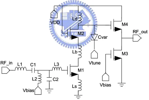
(27) tuning rang exceeds 4GHz, which is great larger than that of 6% in [5], and that of 35% in [6]. Given the target of frequency tuning range over several GHz, the designed LNA requires wideband input impedance matching network different from the inductive source degeneration used in the conventional narrow-band CMOS LNA [3]. In addition, gain level over the entire band must remain as flat as possible. The schematic of the proposed LNA circuit is as shown in Fig. 3.1, consisting of cascode configuration and a source-follower output buffer. The circuit achieves the wideband input matching by a three-section band-pass Chebyshev filter configuration [7]. The inter-stage inductor, Lb, improves gain flatness among sub-bands. A varactor, Cvar, provides frequency tuning capability. Technologies to achieve the wideband tuning and gain flatness are discussed narrowly below.. VDD. Ld M4 M2. RF_out Cvar. Lb RF_in. L1. C1. M3 Vtune. L3 M1. L2 Vbias. C2 Ls. Vbias. Fig. 3.1 Shematic of the poposed ultra-wideband tunable LNA.. 3.2.2 Broadband Matching Techniques The technique of filter design is employed for broadband input impedance matching. The two kinds of the most common used filter design technique are image. 13.
(28) parameter method and insertion loss method. The first one, image parameter method, consists of a cascade of simpler two-port filter sections to provide the desired cutoff frequencies and attenuation characteristics. Thus, although the procedure is relatively simple, the design of filters by image parameter method often must be iterated many times to achieve the desired results and that will result in large chip area. The other one, insertion loss method, uses network synthesis techniques to design filters with a completely specified frequency response. The design is simplified by beginning with low-pass filter prototypes that are normalized in terms of impedance and frequency. Transformations are applied to convert the prototype designs to the desired frequency range and impedance level [8]. The insertion loss method is used to design the broadband input impedance matching for diminishing the implement cost. The Butterworth and Chebyshev filter design are two familiarly practical filter responses by used insertion loss method. The Butterworth design offers a smooth response curve with maximal flatness at zero frequency. The Chebyshev design offers a steeper response curve at the 3 dB cutoff frequency and requires fewer components. In this work, to have precipitous response curve at 3 dB cutoff frequency, the Chebyshev filter design is chosen. The design of a Chebyshev filter will begin at low-pass filter prototypes which are normalized in terms of impedance and frequency; this normalization simplifies the design. The low-pass prototypes are then scaled to the desired frequency and impedance. The design process is illustrated in Fig. 3.2. Filter specifications. Low-pass prototype. Scaling and transformation. Circuit implement. Fig. 3.2 The process of filter design. In the insertion loss method, a filter response is defined by its insertion loss, or power loss ratio, PLR, 14.
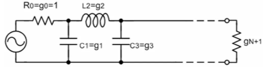
(29) PLR=. Power available from source 1 = , Power delivered to load 1− | Γ(ω ) |2. | Γ(ω ) |2 =. M(ω 2 ) , M(ω 2 ) + N(ω 2 ). (3-1). (3-2). where M and N are real polynomials in ω 2 . Substitute equation (3-2) into (3-1), thus PLR can be re-expressed as PLR = 1 +. M(ω 2 ) . N(ω 2 ). (3-3). In this work, the Chebyshev polynomial is used to specify the insertion loss of an N-order low-pass filter as. PLR=1+k 2T 2N (. ω ), ωc. (3-4). then a sharper cutoff will result. TN (x) Oscillates between ± 1 for x ≤ 1 , and. k 2 determines the pass-band ripple level. From the power loss ratio equation of Chebyshev filter, the normalized element values of L and C of low pass filter prototype can be figured out. The element definitions of the ladder circuits for low-pass filter prototypes is shown in Fig. 3.3, and the normalize values are listed in Table 3.1.. Fig. 3.3 Ladder circuit for low-pass filter prototypes and their element definitions.. 15.
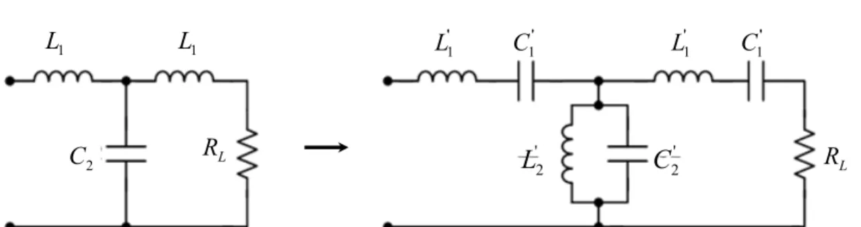
(30) Table 3.1 Element values for Chebyshev Low Pass Filter prototypes (g0=1, ωc =1, ripple=0.5dB). N (order) 1 2 3. g1 0.6986 1.4029 1.5963. g2 1.0000 0.7071 1.0967. g3. g4. 1.9841 1.5963. 1.0000. Low pass filter prototypes design could be transferred to be a band-pass filter response. At the beginning, scale the impedance from unity to the load and source impedance, and also scale the frequency from unity of the low pass prototype to the cutoff frequency of the band-pass one. ω1 and ω2 denote the 3-dB cut-off frequency of the band-pass filter. Thus the band-pass response could be obtained as. ω←. where ∆=. ω0 ω ω0 1 ω ω0 = , ω 2-ω 1 ω 0 ω ∆ ω 0 ω . (3-5). ω 2-ω 1 . The resonant frequency, ω0 , could be chosen equal to the geometric ω0. mean of ω1 and ω2 , that is ω0 = ω1ω2 . The low-pass prototype transfers to the band-pass filter type based on Table 3.1. The low-pass filter elements are converted to series or parallel resonant circuits. The low impedance at resonance, such as a series inductor, Lk, converts to a series LC circuit with element values of Table 3.1, Lk'=. Lk , ∆ω 0. (3-6). ∆ . ω 0Lk. (3-7). Ck'=. The high impedance at resonance, such as a shunt capacitor, Ck, transfers to a shunt LC circuit with element values of Table 3.1, Lk'=. ∆ , ω 0Ck. (3-8) 16.
(31) Ck'=. Ck . ∆ω 0. (3-9). Both series and parallel resonator have the same resonant frequency of ω0 . Fig. 3.4 shows that condition, where Z0 means the source impedance. Fig. 3.5 shows the complete transformation circuit of low-pass filter converted to band-pass filter. Bandpass. Low-pass. LZ 0. ω0 ∆. L. ∆. ω0 LZ 0. (a). C. ∆Z 0. C. ω0C. ω0 ∆Z 0. (b). Fig. 3.4 Components convert from low pass filter to band-pass filter. (a) Series inductor transferred to series LC (b) Parallel capacitor transferred to shunt LC. L1. L1. C2. L1'. RL. C1'. L'2. L1'. C1'. C2'. RL. Fig. 3.5 The transformation circuit of low pass filter converted to band-pass filter. Employ the filter design technique to do the broadband input impedance matching from 6 to 10 GHz. The small signal model of the input matching network is as shown in Fig. 3.6. 17.
(32) Chebyshev filter L1. C1 C2. Zin. L3. gm1V1 + V1 -. L2. Cgs1. Ls. Fig. 3.6. The small signal model of the input impedance. The filter actually makes use of the parasitic gate-source capacitance Cgs. The values of all elements are chosen following the third-order Chebyshev filter design which have discussed above with corner frequencies set to be 6GHz and 10GHz. The input impedance is derived as. Zin = Z1 +. Z 2 (Z3 + ωT Ls ) , Z 2 + Z3 + ωT Ls. (3-10). where Z1 = sL1 +. 1 1 , Z 2 = sL2 // , sC1 sC 2. Z 3 = s ( L3 + Ls ) +. g 1 , ωT = m . sC gs1 C gs1. Similar to narrow-band matching, the source inductor, Ls, results in a real resistive value equal to gmLs/Cgs1 to match with the source impedance of 50ohm. The size of the transistor M1 must be selected carefully. The parasitic capacitance. Cgs1 must follow the required component value in the filter design. On the other hand, the device size must yields to sufficient noise performance and power constraint [9]. It may be necessary to adjust the filter corner frequency and choose a reasonable size in order to meet all the specifications.. 18.
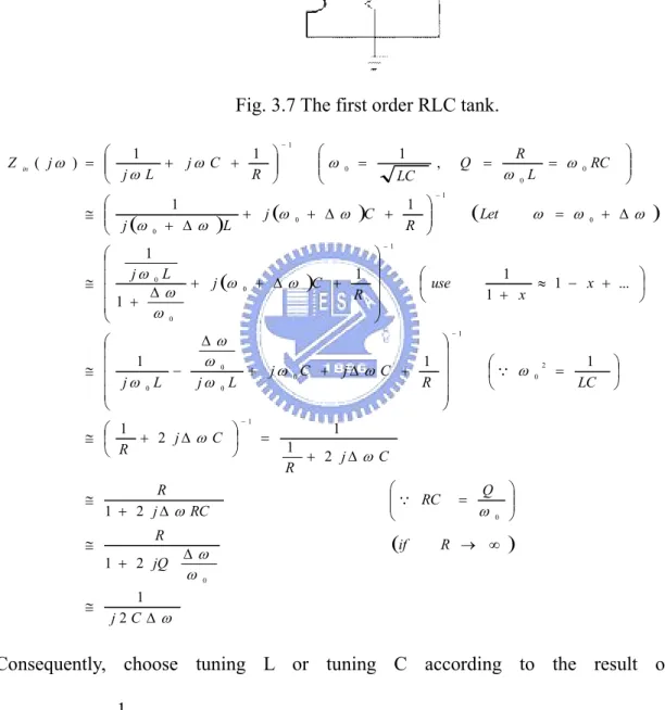
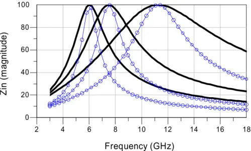
(33) 3.2.3 Tunable RLC Tank The frequency tuning is achieved by the first order RLC tank, as shown in Fig 3.7. Thus we could derive the impedance as below.. Fig. 3.7 The first order RLC tank. Z. in. 1 1 ( j ω ) = + jω C + j L R ω ≅ j (ω. 0. 1 + ∆ω. 1 j ω 0 L ≅ ∆ω 1 + ω 0 . )L. + j (ω. R. 1 LC. =. + ∆ ω )C +. 1 + ∆ ω )C + R . −1. =. 1 R. Q =. , . −1. (Let. . = ω 0 RC. ω = ω. 0. + ∆ω. ). −1. use . Q RC . (if. ∆ω. ω. R. ω 0L. 1 ≈ 1 − x + ... 1 + x −1. Q ω . 2 0. =. 1 LC. . 1 1 + 2 j∆ ω C R. R 1 + 2 j ∆ ω RC 1 + 2 jQ. ≅. 0. 0. 0. ω0 1 + jω 0C + j∆ ω C + R jω 0 L . 1 ≅ + 2 j∆ ω C R . ≅. + j (ω. ω . ∆ω. 1 ≅ − jω 0 L . ≅. −1. =. Q 0 . ω. R → ∞. ). 0. 1 j2C ∆ ω. Consequently, choose tuning L or tuning C according to the result of. Z in ( jω ) ≈. 1 . In this work, sub-band in 500MHz should be selected. Thus, 1 + 2 jC∆ω. the load impedance should not be steep. That is to say the quality of output tunable load must be poor. Larger C will result in narrower selective band. To fix the capacitor value while tuning the inductor, the quality of selective bands independence with 19.
(34) frequency, as shown in Fig. 3.8. If larger C is picked the impedance magnitude will be more precipitous, as the black line shown in Fig. 3.8. Tow of the most used ways for tunable inductors are switching and active inductors. To switch inductors will increase chip area, besides the poor Q resulting from switching parasitic resistors must be considered. There is no such issue in active inductors, but power consumption increase. To maintain low power level, hence a tunable MOS varactor capacitor is chosen to provide frequency tuning. The smaller inductor is chosen to preserve quality factor in the high frequency, as the blue line with circles shown in Fig. 3.9. 100. Zin (m agnitude). 80 60 40 20 0. 2. 4. 6. 8. 10. 12. 14. 16. 18. Frequency (GHz). Fig. 3.8 Fix C and tuning L. (the black line shows the larger C value, and the blue line with circle shows the smaller C value.). 20.
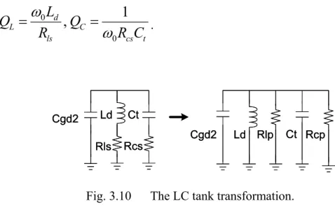
(35) 100. Zin (magnitude). 80 60 40 20 0 2. 4. 6. 8. 10. 12. 14. 16. 18. Frequency (GHz) Fig. 3.9 Fix L and tuning C. (the black line shows the larger L value, and the blue line with circle shows the smaller L value.). In this design, frequency tuning is achieved by a tunable LC tank at the output of the common-gate transistor drain. This resonator consists of a fixed-value inductor and a MOS varactor. To obtain frequency tuning over 6~10GHz, the value of the capacitance in this work varies from 0.46pF to 1.46pF. The equivalent circuit model of the LC tank is as shown in Fig. 3.10, including the gate-drain capacitor, Cgd2, of M2. The resistors Rls, and Rcs, standing for the parasitic of the inductor Ld and the varactor Ct, respectively, degrade the quality factor of the resonator. The resonance frequency and the quality factor are therefore determined as. ω0 =. Q=. 1 Ld (C gd 2 + C t ). Rlp // Rcp. ω0 Ld. ,. (3-11). ,. (3-12). where. Rlp ≈ Rls ⋅ (QL2 + 1) ,. Rcp ≈ Rcs ⋅ (QC2 + 1) ,. 21.
(36) QL =. ω0 Ld Rls. , QC =. Cgd2. 1 . ω0 RcsCt. Ld. Ct. Rls. Rcs. Fig. 3.10. Ct Rcp. Ld Rlp. Cgd2. The LC tank transformation.. 3.2.4 Gain Compensation Technique At resonant frequency, the gain of this LNA is mainly proportional to the LC tank impedance level, which can be derived as ZL =. s ( RLp // RCp ) Ld s ( RLp // RCp ) Ld (C gd 2 + Ct ) + sLd + ( RLp // RCp ) 2. .. (3-13). Higher Q value of the LC tank leads to larger LNA gain. Besides, the impedance level appears to be smaller at lower frequencies. To maintain gain flatness, an inductor Lb is inserted into the cascode stage to enhance the circuit transconductance, Gm1, at lower frequencies. The small signal model of the input stage is shown in Fig.3.11. The Gm1 can be derived as equation (3-14). L1. Vin. C1. L3. g m1 v1 +. C2. L2. V1 −. C gs1. Lb. io. Cx Ls. Fig.3.11 The small signal model of the input stage.. 22.
(37) Gm1 =. io = Vin. − g m /( s 2 Lb C x + 1). Z 2 + Z 3 + ω T Ls , s Ls C gs1 + s ( Ls g m + C gs1 Z 3 + sC gs1 Z1 * ) Z2 2. (3−14). where Z 1 = sL1 +. 1 1 , Z 2 = sL2 // , sC1 sC 2. g 1 , ωT = m Z 3 = s ( L3 + Ls ) + sC gs1 C gs1. ,. Cx is the sum of the gate-to-drain capacitor and drain-to-source capacitor of M1. The factor of ( s 2 Lb C x + 1) is less than one at low frequencies such that Gm1 is enhanced.. 3.2.5 Design Considerations and Trade off This is a tunable low noise amplifier with wideband tunable load and broadband input impedance matching. Since the Cgs of M1 included into the Chebyshev broadband filter design, the capacitance must be around 250fF. Therefore, the size of M1 is selected to conform to the broadband matching issue. In this work, 132.5um width and the 0.18um length are chosen. However, such choice leads to mismatch noise optimum and the low power level. To overcome those issues, another amended circuit is proporsed in section 3.3. In order to compensate the smaller gain at the lower frequency which comes from the poor Q factor of the MOS varactor, the inter- stage inductor Lb included is 1.8nH to enhance the transconductance at 6~7GHz. While load impedance is higher, and then the gain is larger. Therefore, the Q factor of the load inductor, Ld , must be as larger as possible. The technique of layout optimization[9] usd increase the quality factor up to 15~16.. 23.
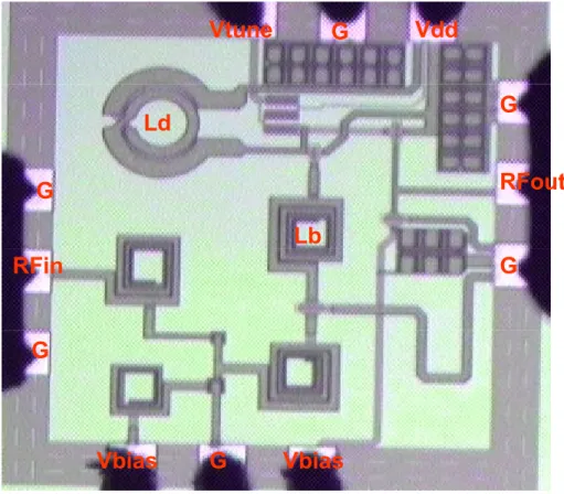
(38) 3.2.6 Consideration of Layout As discussed in Section 3.2.5, the higher Q value of the inductor Ld is, the larger gain of the LNA has. Standard CMOS integrated inductors have inherently low quality factor because of serious substrate losses at GHz frequencies. The technique of layout optimization [9] is used to increase the quality factor. The symmetric two-turn inductors are built on the top most metal layer. The width of the inductor is smaller gradually from the outer circle into the inner circle to increase the internal diameter. The width of the outer circle is larger, 34um, to move the Q peak into 6-10 GHz. The quality factor is larger than 15 at 6-10GHz as shown in Fig. 3.12. 17 16 15. Q. 14 13 12 11 10. 3. 4. 5. 6. 7. 8. 9. 10. 11. 12. freq, GHz. Fig. 3.12 The quality factor of the inductor Ld . The total chip area is 0.897mm by 0.906mm. The RF input and output ports are placed on opposite sides of the chip to improve the isolation of the output to input port. The patterned ground shield is used for reduce substrate noise. All long interconnects should be minimized and built on the most top metal to minimize the substrate loss.. 24.
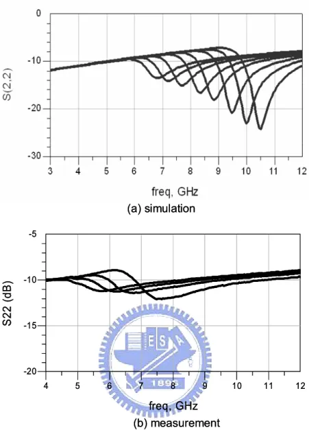
(39) 3.2.7 Microphotograph of Chip The microphotograph of the tunable LNA circuit is shown in Figure3.13. The circuit is fabricated in the TSMC 0.18µm CMOS process technology. The die area including bonding pads is 0.897 mm by 0.906 mm.. Vtune. G. Vdd G. Ld. RFout. G Lb RFin. G. G. Vbias. G. Vbias. Fig. 3.13 Microphotograph of the tunable LNA.. 3.2.8 Simulation and Measurement results and Discussion Measurement is conducted by on-wafer RF probing. Measured results are plotted from Fig. 3.14 to Fig.3.20. Compare with simulation data, the LNA measurement results show narrower tunable range and lower operation frequency over 5.1GHz to 6.8GHz. The measured power gain S21 achieves the maximum value of 7dB at 6.8GHz. Fig. 3.14 shows that condition, the solid black line is the simulation result and the dot gray one the measurement data. The tunable frequency drifts due to. 25.
(40) inconsistency of MOS varactor models in design kit of simulator, ADS, and layout model. The discrepancy is shown in Fig. 3.15. Obviously, the varactor capacitance of the layout model in TSMC document is larger then that of the design kit in ADS simulator. Thus the unconfirmed varactor model used results in the conflict measurement results. To re-simulate the circuit used the affirmed varactor model, and then the tunable frequency matches to the measurement data, as shown in the Fig. 3.16. The input return loss is shown in Fig. 3.17, the black line is the measurement data, and the blue line is the simulation data, and the red line with squares is the simulation with 10% drift of the inductors. After considering the 10% drift of the inductors, L1, L2, Lg, and Ls, and to re-simulate the circuit gets the similar trend to the measurement data. The measurement and simulation result of output return loss, S22, is shown in Fig. 3.18. Fig. 3.19 is the simulation result of noise figure. Since S11 and S21 matched at 6.8GHz only, therefore the noise figure at 6.8GHz is 5.7dB. The linearity analysis is conducted by the two tone test. Fig.3.21 is IIP3 measured data; lower power gain results in higher linearity. The total power of the tunable LNA is 19.51mW with a power supply 1.5V. Table 3.2 is the summary of measured performance and comparison to other tunable amplifier.. 26.
(41) 12. S21 (dB). 7. 2. -3. -8 4. 5. 6. 7. 8. 9. 10. 11. 12. frequency (GHz). Fig. 3.14 S21 simulation and measured result of the tunable LNA. (Solid black line is the simulation result and the dot gray line is the measurement result.) Tuning voltage vs. Varactor capacitor 1.0. Capacitor value (pF). 0.9 0.8 0.7 0.6 0.5 0.4. C_ADS design kit C_TSMC Document Model. 0.3 0.80. 0.90. 1.00. 1.10. 1.20. 1.30. 1.40. 1.50. Tuning voltage (V). Fig. 3.15 The tuning voltage relative to the varactor capacitance. 27.
(42) Tunning voltage vs. Frequency 11.0 sim._Cvar_w/design kit measurement sim._Cvar_w/document. Center frequency (GHz). 10.0 9.0 8.0 7.0 6.0 5.0 0.80. 0.90. 1.00. 1.10. 1.20. 1.30. 1.40. 1.50. Tuning voltage (V). Fig. 3.16 The tuning voltage relative to the center frequency. (the blue line with diamonds is the simulation with the ADS design lit, and the red line with triangles is the simulation with the model in TSMC document, and the green line with stars is the measurement data.). 0. S11 (dB). -10. -20. Measurement Simulation Trouble shooting. -30. -40. 3. 4. 5. 6. 7. 8. 9. 10. 11. 12. Frequency (GHz) Fig. 3.17 S11 simulation and measured result of the tunable LNA.. 28.
(43) (a) simulation. S22 (dB). -5. -10. -15. -20. 4. 5. 6. 7. 8. 9. 10. 11. 12. freq, GHz (b) measurement. Fig. 3.18 S22 simulation and measured result of the tunable LNA. (a) The simulation result (b) The measurement result. 29.
(44) Fig. 3.19 Noise Figure simulation result.. IIP3 (dBm). 5 4 3 2 1 0 -1 -2. 模 擬IIP3 IIP3 Simulation Measurement IIP3 量 測 IIP3. -3 -4 -5 0.9. 0.95. 1. 1.05. 1.1. 1.15. 1.2. 1.25. 1.3. 1.35. 1.4. 1.45. Tuning Voltage (V). Fig. 3.20 IIP3 versus frequency simulation and measured result.. 30. 1.5.
(45) TABLE 3.2 Summary of measured performance and comparison to other tunable amplifier Performance. Summary and Comparison [5] Measurement ISCAS 02. 13.2 dB. [6] VLSI 04 0.25um CMOS IBM 11.7 dB. -5.3dB. <-10dB. -10.3dB. <-24dB. 5.7dB (at 6.8GHz). 2.59 dB. 2.6 dB. 1.15 dBm. 3.2 dBm. -3.98 dBm. 6.0 ~ 10.0 GHz. 5.1~6.8 GHz. N/A 5.6 ~ 5.96 GHz. 50%. 28%. 6%. 35%. 19.6 mW. 19.51 mW. 22.2 mW. 40 mW. Simulation. Technology. 0.18um CMOS Standard. S21(max). 11.6 dB. <-12dB. 7 dB (at 6.8GHz) <-4 (5~7GHz) <-9 (7~11GHz) <-10 (5~7GHz). S11. <-9dB. S22 NF(average). 4.75 dB. IIP3(average) Center Frequency tuning range Frequency tuning ratio Power consumption. 31. 1.4 ~ 2.0 GHz.
(46) 3.3 Improved 6 to 10GHz UWB Tunable LNA Discussed in section 3.2, the frequency tunable range is narrower then simulation one. The tunable LNA is revised as shown in Fig. 3.21. The amended circuit incorporates not only enhanced band tuning range but also broadband impedance matching to improve noise performance. Since the input broadband matching in the previous circuit, Chebyshev filter design is used. The gate to source capacitor of the transconductance stage is included to consist of the Chebyshev filter. Thus, the noise optimum mismatched as mentioned in section 3.2. The revised circuit achieves wideband input impedance matching by the resonance matching technique. L1 and C1 are used to improve the input impedance matching bandwidth. A varactor, Cvar, and a switch capacitor, Csw, provide frequency tuning capability. M1 and M2 consist of cascode configuration to minimize the miller effect and to improve the isolation between the tunable load and broadband input impedance. M3 and M4 implement a source- follower output buffer. R1 and R2 are used to bias the buffer and the bypass capacitor is put on the gate of M4 to be an ac ground path. The transconductance (Gm) of the input stage must be designed to compensate the gain discrepancy between sub-bands.. 32.
(47) VDD C pass. Ld. M3. M2. RFin. Lg L1. C pad. C1. C var. RF out. C sw R 1 M sw. M1. M4. Vtune. Ls. Vsw. V gs. R2. C pass. Fig. 3.21 The amended UWB tunable LNA schematic. 3.3.1 Frequency Tunable Mechanism The frequency tuning is enhanced by a switched capacitor at the output tunable load. This resonator consists of a fixed-value inductor, a tunable MOS varactor and a capacitor serial with the switching transistor. The equivalent circuit model of the tunable load is as shown in Fig. 3.22 (a), including the gate-drain capacitor, Cgd2, of M2. The resistors Rls, and Rcs, standing for the parasitic of the inductor Ld and the varactor Cvar, respectively, degrade the quality factor of the resonator. While tuning the operation frequency in low band, the switch transistor must be turned on and the channel of Msw will induce a parasitic resistance, Rgms, and a overlap capacitor, Covgd, as shown in Fig. 3.22 (b). At Msw turned on, the ac current will flow through Rgms, as the red line shown in Fig. 3.22 (b) because of the impedance of Rgms much smaller then Covgd. When Msw turns off, the overlap capacitor, Covgd, is series with Csw resulting in a small capacitor to operate at high frequency 33.
(48) tuning, as shown in Fig. 3.22 (c). Fig. 3.22(b) and (c) could be expressed in parallel form as Fig. 3.22 (d) and (e) respectively. The capacitor Ctot1 equals to Cgd2 plus Csw and Ctot2 equals to Cgd2 plus Csw series with Covgd. The resonance frequency and the quality factor are therefore determined as 1. ω 0 _ swon =. Ld (Ctot1 + C var ) 1. ω0 _ swoff =. Qswon =. Qswoff =. Ld (Ctot 2 + C var ). Rlp // Rcp // Rgmp. ω0 Ld Rlp // Rcp. ω0 Ld. ,. (3-15). ,. (3-16). ,. (3-17). ,. (3-18). where. Rlp ≈ Rls ⋅ (QL2d + 1) , QL = d. ω0 Ld Rls. ,. QC = var. Rcp ≈ Rcs ⋅ (QC2 var + 1),. Rgmp ≈ Rgms ⋅ (QC2 sw + 1). , (3−19). 1 1 , QC = . ω0 RcsCvar ω0 RgmsCsw. (3−20). sw. Cgd2. Ld. Cvar. Csw Ctot1. Cvar. Ld. Rlp Rls. Covgd. Cgd2. Ld. Cvar. Rgms. Csw. (b) switch trun on Rls. Rcp. Rcs. Rcs. (d) switch trun on. Msw Vsw. Cgd2. Ld. Cvar. Csw Ctot2. (a). Ld. Cvar Rlp. Rls. Rcs. Covgd. (c) switch trun off. Fig. 3.22 The tunable mechanism. 34. (e) switch trun off. Rcp. Rgmp.
(49) 3.3.2 Resonance Matching Technique The input impedance small signal model is as shown in Fig.3.23, the well-known narrow band impedance can be derived as Z, which the impedance trend in smith chart is shown as the solid line in Fig. 3.24. At the resonant frequency, ω0 , impedance of Z is matched to 50 ohm, and while the operation frequency is upper than the resonant frequency, Z characters an inductive impedance, and otherwise characters a capacitive impedance. Tank, L1 and C1 is added to provide capacitive impedance in the upper operation frequency to compensate the inductive one, and the same compensation technique is in the lower operation frequency. The impedance compensation trend is the dot line, Z’ , as shown in Fig. 3.24. The broad band input impedance matching is achieved by the resonance technique.. Fig. 3.23 The input impedance small signal model. 1 Z = Lsωt + j ωLs + ωLg − ωC gs1 . 1 Z = jωC1 + jωL1 '. −1. ω0 =. (L. s. .. 1. ). + Lg C gs1. ,. (3-21). (3-22). 35.
(50) ω2> ω0 (inductive + j X ). Z-Smith Chart (capacitive − j X ). Real axis of the Smith chart. ω0 (inductive + j X ). (capacitiv e − j X ). ω1< ω0 Fig. 3.24 The impedance trend in smith chart.. 3.3.3 Design Considerations and Trade off As mentioned in section 3.3.1, the tunable load impedance is different from the switch transistor turned on or off. Thus the gain of tunable LNA in this work is mainly proportional to the LC tank impedance level at resonance frequency, which can be derived as s ( RLp // RCp // Rgmp ) Ld. Z L _ swon =. s ( RLp // RCp // R gmp ) Ld (Ctot1 + C var ) + sLd + ( RLp // RCp // Rgmp ) 2. Z L _ swoff =. s ( RLp // RCp ) Ld s ( RLp // RCp ) Ld (Ctot 2 + C var ) + sLd + ( RLp // RCp ) 2. .. ,. (3-23). (3-24). To compare equation (3-23) with (3-24), there is smaller load impedance at low frequency due to the parasitic resistance of switched transistor, Rgmp. The smaller load impedance level leads to the low power gain. Thus, the power gain at low frequency is enhanced by boosted the transconductance, Gm1, of M1 at 6-to-7 GHz. The Gm1 could be derived as Gm1 =. ω02 io , = − g m1 ω0 vi 2 2 + ω0 s +s Q. (3-25). 36.
(51) ω0 =. 1 C gs1 ( Ls + Lg ). , Q=. 1 . ω0 g m1Ls. (3-26). Obviously, Gm1 is shown as a second order low pass filter. The Q value of that filter is designed to enhance Gm1. Besides Gm1 to be augmented for low gain level, the high Q value of the LC tank also leads to large LNA gain. Thus, how large the parasitic resistance is must be concerned while the size of switched transistor is chosen. The larger size of switched transistor is, the smaller parasitic resistance is. But the large size of Msw leads to large overlap capacitor, Covgd. That will result in the large capacitor of Ctot2 at Msw turned off, as shown in Fig 3.22(e), which comes the operation frequency drift to lower then what designed. In this work, the size of Msw would be chosen at 87.5um width and 0.18 lengths. In this work, the Cgs of M1 does not be included into the broadband filter design and the noise optimization could be achieved. The noise figure is optimized to be 3.23-to-3.8 dB. The source- follower buffer is biased by the voltage divided of R1 and R2. The process variation of resistors must be concerned to make sure the output buffer satisfied the output impedance matching to 50 ohm for measurement.. 3.3.4 Consideration of Layout The higher Q value of the inductor Ld is, the larger gain of the LNA has. The small inductor leads to the Q peak at higher frequency. In this work, small inductor value of 0.5nH is used. In order to move the Q peak into 6- to 10 GHz, the width of Ld is 34um. The total chip area is 0.825mm by 0.94mm. The RF input and output ports are placed on opposite sides of the chip to improve the isolation of the output to input port. The patterned ground shield is used for reduce substrate noise. Except Ld , all other inductors are used by the layout of TSMC supported. All long interconnects should be minimized and built on the most top metal to minimize the substrate loss. 37.
(52) All interconnects of the DC voltage supply has bypass capacitors to be ac ground path to reduce the parasitic inductances.. 3.3.5 Microphotograph of Chip The microphotograph of the tunable LNA circuit is shown in Figure3.25. The circuit is fabricated in the TSMC 0.18µm CMOS process technology. The die area including bonding pads is 0.825 mm by 0.94 mm.. Vgs. GND. VDD. GND. L1. Ld. GND. RFin Cvar. GND. L2. RFout. Csw Msw. Ls. Vtune. GND. GND. Vsw. Fig. 3.25 Microphotograph of the amended tunable LNA.. 3.3.6 Simulation and Measurement results and Discussion Measurement is conducted by on-wafer RF probing. Measured results are plotted as shown from Fig. 3.26 to Fig.3.29. The LNA measurement shows frequency tunable range from 6.3GHz to 9.3GHz, which is smaller then design due to 100fF 38.
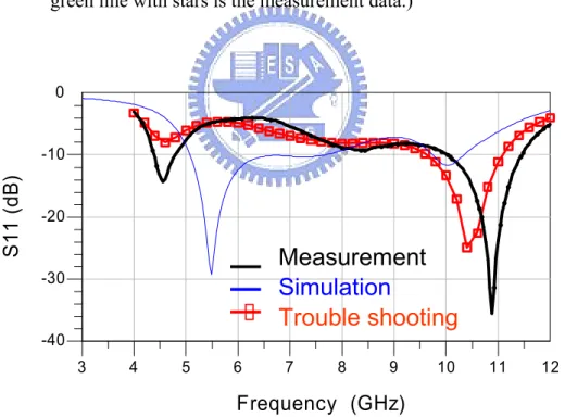
(53) parasitic capacitance in the layout of the tunable LC tank load. The measured power gain S21 achieves the maximum value of 9.3dB at 9.4GHz. According to equation (3-23), while the parasitic resistance of the switched transistor is large and thus the power gain will become small. The measured gain is larger at high frequency then at low frequency due to Cgs1 of M1 is smaller then designed; thus comes at Gm1 enhanced at high frequency. Fig. 3.26 shows the condition. The input return loss is shown in Fig. 3.27. As we mentioned in section 3.3.4, all the metal lines of DC bias supply need bypass capacitors to be ac ground path to reduce the parasitic inductance. However, the metal line of the gate bias for M1 had been left out to add the ac ground path. The parasitic inductance of 10pH needs to be added. 10fF of layout parasitic capacitor of C1 also has to be included. The smaller Cgs1 of M1, the added parasitic inductance and the capacitance are all together included to re-simulate the input impedance, and thus the input impedance trend is more matched to measurement results. The measurement and simulation result of output return loss, S22, is shown in Fig. 3.28. Fig. 3.29 is the simulation and measurement result of noise figure. The linearity analysis is conducted by the two tone test. Fig.3.30 is the IIP3 measured data. The total power of the tunable LNA is 17.44mW with a power supply 1.5V.. Table 3.3 is the summary of measured. performance and comparison to the previous tunable amplifier.. 39.
(54) 18. Switch on. Switch off. S21 (dB). 15. 10. 5. 0 5. 6. 7. 8. 9. 10. 11. Frequency (GHz) (a) S22 Simulation 11 10. Switch on. Switch off. S21 (dB). 8 6 4 2 0 5. 6. 7. 8. 9. 10. 11. Frequency (GHz) (b) S22 measurement Fig. 3.26 S21 simulation and measured result of the amended tunable LNA, (a) is the simulation result and (b) is the measurement result.. 40.
(55) 0. -10 -15. Sim. Sim. w/ troubleshooting Meas.. -20 -25. 2. 4. 6. 8. 10. 12. Frequency (GHz) (a) S11 measurement and simulation results. S11. S11 (dB). -5. Sim. Sim. w/ troubleshooting Meas. freq (2.000GHz to 12.00GHz). (b) S11 smith chart. Fig. 3.27 S11 simulation and measured result of the amended tunable LNA, (a) S11 measurement and simulation results and (b) S11 smith chart trend.. 41.
(56) -5 -10. S22 (dB). -15 -20 -25 -30 -35 -40 6. 7. 8. 9. 10. 11. freq, GHz. (a) S22 simulation -5 -6. S22 (dB). -8 -10 -12 -14 -16 6. 7. 8. 9. 10. 11. Frequency (GHz). (b) S22 measurement Fig. 3.28 S22 simulation and measured result of the amended tunable LNA. (a) The simulation result, (b) The measurement result.. 42.
(57) 8. NF (dB). 7 6 5 4 3 4. 5. 6. 7. 8. 9. 10. 11. freq, GHz (a) NF simulation 10 9. NF (dB). 8 7 6 5 4 3 0. 2. 4. 6. 8. 10. 12. 14. Frequency (GHz). (b) NF measurement Fig. 3.29 Noise Figure of the amended tunable LNA. (a) simulation result (b) measurement result.. 43.
(58) -4 -5 -6 IIP3 (dBm). -7 -8 -9 -10 -11. Meas. Sim.. -12 5. 6. 7. 8. 9. 10. 11. 12. Frequency (GHz). Fig. 3.30 IIP3. TABLE 3.3 Summary of measured performance and comparison to the previous tunable amplifier. Technology. Summary and Comparison Section 3.2 This work Measurement Simulation 0.18um TSMC CMOS Standard. Supply voltage. 1.5V. Performance. Section 3.2 Simulation. S21(max). 11.6 dB. S11. <-9dB. S22. This work Measurement. 14.9 dB. 9.3 dB. <-11dB. <-6dB. <-12dB. 7 dB (at 6.8GHz) <-4 (5~7GHz) <-9 (7~11GHz) <-10 (5~7GHz). <-15dB. <-10 dB. S12. <-38 dB. < -40(5~7GHz). <-40 dB. <-41 dB. NF(average). 4.75 dB. 5.7dB (at 6.8GHz). 3.5 dB. 4.5 dB. IIP3(average) Center Frequency tuning range Frequency tuning ratio Area. 1.15 dBm. 3.2 dBm. 6.0 ~ 10.0 GHz. 5.1~6.8 GHz. -10 dBm 6.3 ~ 10 GHz. -6 dBm 6.3 ~ 9.4 GHz. 50%. 28%. 45.3%. 39.5%. Power consumption. 0.813 mm2 19.6 mW. 19.51 mW. 44. 0.776 mm2 17.4 mW. 17.44 mW.
(59) 3.4. A Tunable LNA with MEMES Inductors for UWB Mode-2 Device. 3.4.1 Motivation As mentioned in section 3.2, to do the wideband frequency tuning could be achieved by switching capacitors or inductors while those components have high quality factors. Nowadays, the high performance of micromachined spiral inductors has been proposed [10]. The inductor with the underneath substrate removal has four times quality factor improvement than the conventional one. The suspended inductors with the cross membrane supporting and the underneath substrate removal have not only high Q performance but also better reliability for wideband application [11]. To do frequency tunable range from 3.1 GHz to 8 GHz, there is congenital limitation by only using MOS varactor as discussed in section 3.2. To enhance the tunable range with switched capacitor is proposed in section 3.3, but this way the poor quality factor of large capacitance will degrade the gain at low frequency. Thus, to maintain gain flatness over 5GHz is a critical consideration. In this section, switched micromachined inductors and MOS varactor used to make the frequency tunable capability. To integrate micromachined inductors with the chip die of 0.18um CMOS process, the thermo- compression boding technique is used. The LNA of frequency tuning range over 5 GHz, low noise performance and low power consumption is proposed.. 3.4.2 Circuit Architecture The schematic of the proposed LNA circuit is similar to that in section 3.2, as shown in Fig. 3.31, exception the inductor switched mechanism and the external capacitor parallel with Cgs of M1 included. The wideband input matching by a three-section band-pass Chebyshev filter configuration consists of L1, L2, Lg, Ls, C1,. 45.
(60) C2, Cex and Cgs of M1, where Cex provides enough capacitance for satisfying the filter design issue. Micromachined inductors, L1, L2, and Lg have small parasitic resistance due to substrate lossless with underneath substrate removal. Thus, the thermal noise will be decreased apparently. Msw is used to switch inductors. A large resister Rb is employed to provide high impedance for reducing the overlap parasitic capacitances. The micromachined inductor, Ld1, is utilized to provide high power gain. M3 and M4 implement a source- follower output buffer. R1 and R2 are used to bias the buffer.. Vtune M sw. Vsw. VDD. Ld 2. Ld 1. R1 C var. M3 M2. RFin. L1. M4. Lg. C1. L2. M1. C2 C ex. R2. Ls. V gs. Fig. 3.31 The schematic of the tunable LNA for 3~8 GHz. (Where inductors with dot line are MEMS fabricated.). 46. RF out.
(61) 3.4.3 MEMS Inductors The micromachined inductor is fabricated with underneath substrate removal to decrease the substrate loss at high frequency and that will provide a high quality factor inductor. However, the micromachined passive components tend to be affected by the external disturbance, such as air pressure, mechanical thermal force and gravity, etc. Thus, the suspended inductors with the cross membrane supporting are proposed to increase the reliability of the micromachined inductors [11]. The suspended inductor with the cross membrane supporting high Q performance of micromachined spiral inductors is shown in Fig. 3.32, and the cross view of the cross membrane inductor is shown in Fig. 3.33. The measurement result of high Q inductors is shown in Fig.3.34. The measurement shows that the Q of inductor can achieve 45, while the inductor value is around 4nH at 4~8GHz. The amazing good performance is expected to improve the circuit design for radio frequency.. Fig. 3.32 The suspended inductor with the cross membrane supporting. 47.
(62) Fig. 3.33 The cross view of the cross membrane inductor.. Fig. 3.34 The measurement result of the cross membrane inductor. (Where S denotes suspend, M denotes membrane and CM denotes cross membrane.). 3.4.4 Ultra Wide-band Tunable Load The tunable load with switched capacitor, as shown in Fig. 3.35(a), is discussed in section 3.3. The power gain is proportion to Q value of the load as mentioned in section 3.3. Therefore, using switched capacitor can not maintain gain flatness due to Q degraded for a large capacitor at low frequency. High Q MEMS inductors are used to maintain gain flatness over several GHz. Output tunable load with switched inductor consist of Ld1, Ld2 and Msw, as shown in Fig. 3.35(b).. 48.
(63) Vtune Csw. Cvar. L. Vdd. Ld2. Msw. Vtune. Vsw. Cvar. Msw Ld1. Vsw. (a). (b). Fig. 3.35 The tunable mechanism (a) the switched capacitor, (b) the switched inductor. The equivalent model of switched inductors is shown in Fig. 3.36, where Rb is included to reduce the overlap parasitic capacitor. Fig. 3.36 (a) shows the equivalent model of switched transistor turned on. When Msw turns on, the signal current will flow as the blue line path. Otherwise, while Msw turns off, it will be the red path as shown in Fig. 3.36 (b).. Fig. 3.36 The effected inductor, (a) switch turned on, (b) switch turned off.. When Msw turns on, the effected inductance is as Leff _ swon ≈ Ld 1 , Qeff _ swon =. ωLd 1 . R p + Rls. (3-27). Rls is the parasitic resistance of Ld1. The Q value of effected inductor will degrade by Rls and Rp. As mentioned in section 3.1, Q values of L and C will affect the load 49.
(64) impedance level. Therefore, the high Q micromachined inductor, Ld1, is used to maintain high enough load impedance. While Msw turns off, the effected inductor value is as Leff _ swoff (ω ) = Ld 1 +. Ld 2 1 − ω 2 Ld 2 Covp. .. (3-28). Obviously, there is a self resonant frequency ω self = Ld 2Covp . The self resonant frequency must move over the operating frequency to diminish the effect, as shown in Fig. 3.37. Small Covp results in high self resonant frequency. Small Covp indicates small size of Msw, which will increase the parasitic resistance Rp. Therefore, the optimum size of Msw is a critical design in this work. 1.20E-9. 4E-9. 1.18E-9. 3E-9 2E-9. 1.14E-9 1E-9. 1.12E-9. Lswoff. L. 1.16E-9. 0. 1.10E-9 1.08E-9. -1E-9. 2. 4. 6. 8. 10. 12. 14. 16. freq, GHz Fig. 3.37 The equivalent inductor value.. 3.4.5 Noise Considerations The broadband input matching approach in section 3.2 is trade off by the noise performance and the power consumption. To improve the noise performance, the high Q micromachined inductors are used in input broadband matching to decrease the thermal noise. The external capacitor parallel with Cgs of M1 is applied 50.
(65) for power level decreasing. The noise model of NMOS with external capacitor is shown in Fig. 3.38(a), and the small signal model is in Fig. 3.38(b). The equivalent noise voltage and current source are derived as equation (3-29) and (3-30) for without and with external capacitor, respectively. vrg. NM. Cex. iout. Rg. C gs. ing. Cex (a). g mVgs. en ind. noiseless. in. (c). (b). Fig. 3.38 The noise model, (a) NMOS with external capacitor, (b) the small signal noise model, (c) the equivalent noise model. i n = i nd e n = i nd. sC. gs. + i ng. gm. 1 + sC. i n _ c ex = i nd e n _ c ex = i nd. gs. Rg. gm sC. + i ng R g + v rg. (1 + sC. gs. gm. 1 + sC. gs. gm. Rg. t. Rg. )C. ex. Ct. .. (3-29). + i ng (1 + sC. ex. R g ) + v rg sC. ex. + i ng R g + v rg. ,. (3-30). where Ct = C gs + Cex . Let the value of the gate- to- source capacitor is fixed. Compare with two conditions, in _ C. ex. is obviously smaller then in because of. Cex Ct. lower then unity. And en _ C. ex. is. also smaller then en due to that Cgs with Cex is smaller then Cgs without Cex. Thus, conclude that the noise will be decreased by external capacitor added.. 51.
(66) 3.4.6 Consideration of Layout To test the DC current, the consideration schematic and layout is shown in Fig. 3.39 and Fig. 3.40. In Fig. 3.39, the dot line pad, VDD_DC and Vgs_DC, is only for DC current test. The dot line between Ld2 and drain of M2 is used for DC current path of testing and it will be moved by laser cut. Another dot line between gate of M1 and pad, Vgs_DC, is used to bias M1, and will be removed too. L1, L2, Lg, and Ld1 are fabricated in micromachined inductors. In order to bond the chip die with the micromachined inductors, the passivating layer is drawn on the connected point. All interconnect metal lines are considered for circuit design.Fig.3.40 shows the layout of the chip die.. Fig. 3.39 Schematic of the tunable LNA fabricated on the chip die. 52.
(67) L1. L2. GND Lg. Ls. Vgs_DC. GND. VDD_DC Ld1. Ld2 GND. Fig. 3.40 Layout of the chip die. 53.
(68) 3.4.7 Package Integrated Technique The complete layout of this work is shown in Fig. 3.41. All the ground pads are connected together to have the same reference plan for the chip die and the micromachined inductors mask. The thermo- compression bonding is used as shown in Fig. 3.42. The temperature is better at 3750C for fusing the connected gold metal layer. GND L1. L2 Vgs. RFin GND GND Ls Lg. Vtune GND. GND. RFout Ld1. Ld2 GND. VDD. Vsw GND. Fig. 3.41 Layout of the complete integrated circuit. 54. Vtune.
(69) Flip-Chip Micromachined inductor. M6 Gold Copper. Si substrate Substrate removal. Fig. 3.42 The bonding technique. 3.4.8 Simulation results and Comparison Lastly, the simulation results and compare with that similar circuit with switched MIM capacitor summarized in section 3.2. Table 3.4 shows that.. TABLE 3.4 Summary of simulation performance and comparison to the circuit of section 3.2 Summary and Comparison Circuit of Section 3.2 Circuit of this work Simulation Simulation Switched with MIM Cap. Switched with MEMS Ind. 0.18um TSMC CMOS Standard. Performance Technology Supply voltage Center Frequency tuning range S21(range). 6.5~11.1 dB. 11.7~13.2. S11. < -9.5 dB. <-10 dB. S22. <-12 dB. <-14 dB. S12. <-38 dB. <-36 dB. NF(average). 6.2 dB. 3.5 dB. IIP3(average). ~ 0 dBm. ~ -5 dBm. Power consumption. 21.5 mW. 10.5 mW. *FOM(worse case). 0.156. 0.302. ∗ FOM LNA =. 1.5V 3.1 ~ 8 GHz. G[abs] ⋅ IIP3 [mW] ⋅ f[GHz] (NF − 1 )[abs] ⋅ PD [mW]. 55.
(70) Chapter 4 Conclusion The wideband tunable LNA apply for the receiver path of UWB system was proposed and the amended tunable circuit for band tuning capability was also fabricated in standard TSMC 0.18µm CMOS process. The tunable LNA achieved tunable frequency range over 6.3 GHz to 9.3 GHz. To enhance the tunable range and to improve the noise performance, the high Q MEMES inductors were integrated with the tunable low noise amplifier in the third circuit. The tunable LNA circuit with MEMS inductors was proposed in low power level and achieved ultra- wideband frequency tunable range over 3.1GHz to 8GHz and average noise figure of 3.5dB in 10.5 mW power used.. Chapter 5 Future Work The wideband tunable LNA with MEMS inductors for UWB Mode-2 device is taped out. While the measurement is consistent with the target proposed, the circuit can extended to a wideband tunable front- end receiver for UWB system in low noise and low power performance.. 56.
數據
![Fig 2.1 Common LNA architectures. (a) Resistive termination (b) 1/g m termination (c) Shunt - series feedback (d) Inductive degeneration [3]](https://thumb-ap.123doks.com/thumbv2/9libinfo/8471442.183552/21.892.211.618.474.884/common-architectures-resistive-termination-termination-feedback-inductive-degeneration.webp)
+7
相關文件
• Learn the mapping between input data and the corresponding points the low dimensional manifold using mixture of factor analyzers. • Learn a dynamical model based on the points on
Variable gain amplifier use the same way to tend to logarithm and exponential by second-order Taylor’s polynomial.. The circuit is designed by 6 MOS and 2 circuit structure
首先,在前言對於為什麼要進行此項研究,動機為何?製程的選擇是基於
Abstract - A 0.18 μm CMOS low noise amplifier using RC- feedback topology is proposed with optimized matching, gain, noise, linearity and area for UWB applications.. Good
In response to the twenty-first century’s global economy, “broadband network construction” is an important basis for the government in developing the national knowledge and
Finally, making the equivalent circuits and filter prototypes matched, six step impedance filters could be designed, and simulated each filter with Series IV and Sonnet program
It allows a much wider range of algorithms to be applied to the input data and can avoid problems such as the build-up of noise and signal distortion during processing.. Since
The neural controller using an asymmetric self-organizing fuzzy neural network (ASOFNN) is designed to mimic an ideal controller, and the robust controller is designed to
