Lin, Chen, and Jen: Low Power Design for MPEG-2 Video Decoder 513
LOW POWER DESIGN
FOR
MPEG-2 VIDEO DECODER
Chia-Hsing Lin, Chen-Min Chen, and Chein-Wei Jen
Department
ofElectronics Engineering and Institute
ofElectronics
National Chiao Tung University, HsinChu, Taiwan,
ROCABSTRACT
The I/O power consumption in MPEG-2 decoder is significant because of the wide connection with large capacitances to the frame buffer. T o reduce the power dissipation on the Memory Bus, the Gray code encoding scheme is proposed to increase the correlation of the image data transferred on the bus. The bit switching probability in the re-coded data will then decrease and in turn the bus power consumption will be reduced. Combined with the proposed bus arbitration and scheduling scheme proposed in this paper, 22% reduction of power dissipation may be achieved.
I.
INTRODUCTIONI S 0 standard 13818-2[1] known as MPEG-2 (Moving Pictures Expert Group) has been adopted in many applications like DVD Player, set-top boxes and entertainment machines. Because the required computing power for this algorithm is huge, a high performance VLSI solution to the MPEG-2 video decompression is necessary. To promote the success of this motion picture standard, the cost in the video decoding system should also keep low. Usually, the key components in a low cost MPEG-2 decoding system includes a high performance sjngle chip MPEG-2 decoder VLSI and the associated frame buffer DRAM.
Although most MPEG-2 applications belong to the non- portable ones, the cost of providing power and associated cooling indicates that the power reduction is still necessary for non-portable applications[2]. Several approaches to reduce the power consumption for the video decoding system has been proposed[3][4]. In [3] the circuit approach using low-power ASIC RAMS as the on-chip I/O buffers with Selective Bit Line Precharge (SBLP) scheme is adopted to reduce the bit line current. In [4] a low-power approach at architectural level is proposed to reduce power consumption for MPEG functional unit like DCT. The power reduction of on-chip buffers and functional units in MPEG-2 decoder can be achieved using these approaches. However, because of the nature of inter-frame coding in the MPEG-2 video decompressing algorithm, there must offer enough memory bandwidth for single-chip MPEG-2 decoder to perform all the frame buffer access. The fast and wide memory bus between decoder chip and frame buffer
DRAM will cause a significant power consumption because of large capacitance involved at the I/O. Thus, it is also necessary to explore approaches to decrease the I/O power dissipation.
In this paper, we propose some architectural approaches to reduce power consumption for the I/O bus. This strategy has been adopted in the MPEG-2 Video Decoder Chip we designed[5]. In section I1 we first give an overview to our MPEG-2 video decoder VLSI. According to the static characteristics of data on the Memory Bus, the Gray code encoding scheme to reduce the circuit switching activity is described in section 111. In Section IV we describe the bus arbitration and scheduling strategy to preserve the static characteristics of data while transferring them dynamically on the Memory Bus. Section V concludes this paper.
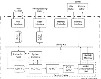
11. THE MPEG-2 VIDEO DECODER A. System Architecture
Fig. 1 shows the block diagram of our MPEG-2 video decoder VLSI. Together with four 4M-bit DRAM and some video post-processing components, a complete video decoder system for MPEG-2 video at main profile and main level (MPOML) can be constructed.
The Decoding Pipeline consists of three functional blocks: variable-lengthhun-length decoder (VLD-RLD), inverse quantizatiodinverse cosine transform unit (IQ- IDCT), and motion compensation/interpolation unit (MC- Interpolator). These functional units can perform the main MPEG-2 decompression algorithm. The RISC-based System Controller can control all other associated functional blocks according to the system parameters issued by host system and the programs stored in instruction RAM. Also; it parses the header information of MPEG-2 bitstream and performs the error concealment routines while error bitstream is encountered. Under the control of System Controller, the decoding pipeline can decode the variable- length-coded information in the MPEG-2 bitstream.
According to the parameters from MPEG-2 bitstream header, the Memory Controller can set up the suitable addresses to load reference pictures. Also, it stores reconstructed picture and loads display picture. It also manages a circular buffer located in external DRAM as the video rate buffer (VBV buffer). The external DRAM, which
514 IEEE Transactions on Consumer Electronics, Vol. 42, No. 3, AUGUST 1996
is connected to the Memory Controller via the DRAM interface, is used to hold the VBV buffer and store decoded frames.
This chip has two internal buses. The 64-bit Memory Bus is used to deliver the incoming MPEG-2 bitstream and decoded pictures. All data transfers to and from the external DRAM pass through this data bus. The control commands between the System Controller and other functional blocks are issued via the 16-bit RISC Data Bus.
B. MPEG-2 Decoding Process follows:
The steps to decode the MPEG-2 bitstream are listed as
Coded bitstream supplied CO the Host Interface i s
written to the VBV buffer
on external DRAM
through the bitstream FIFO and Memory Bus. The transfer is initialized by host system.Coded bitstream is then read out from the VBV buffer, via VLD FIFO, to the VLD-RLD. If the incoming bits belong to the high layer fixed-length coded data (e.g., sequence header, GOP header, picture header and slice header as defined in MPEG-2), they will be then forwarded to System Controller to extract the decoding parameters. On the other hand, if variable-length codes (macroblock header or quantized dct coefficients) are encountered, they will be decoded in the VLD-RLD under the control of System Controller. The decoded DCT coefficients will then be transferred
System Controller first sets up the address of current macroblock for the Memory Controller and checks the type of this macroblock. If the current macroblock is non-intra coded, System Controller also has to calculate the actual motion vectors and set up the addresses of reference macroblocks for the Memory Controller for this non-intra macro- block.
The quantized DCT coefficients are first de- zigzagged and inverse-quantized in IQ unit. Then those values are passed to IDCT unit to recover to the original pixel values or DFD. Finally, the output will be fed to MC-Interpolator.
For non-intra macroblock, MC-Interpolator initializes a memory transfer through Memory Interface to load the reference macroblocks from reference Picture Buffer on external DRAM to the Reference MB buffer. The addresses of these macroblocks are derived by the motion vectors. Interpolation will be needed if motion vectors are given in the half-pel boundary. After MC- Interpolator adds the data of IDCT results and reference macroblock, it will then write the reconstructed blocks to the Picture Buffer on external DRAM. On the other hand, MC- to IQ-IDCT.
Interpolator will forward the IDCT results to the Picture Buffer if intra-coded macroblock is encountered.
6) After decoding one frame, the reconstructed image is re-read from the Picture Buffer according to a specified format and output to the video subsystem outside the decoder chip through Video Interface.
111. BUS POWER REDUCTION
A .Bus
Power ConsumptionIn order to reduce the number of DRAMS and the number of
I/O
pins, the VBV Buffer and Picture Buffer share the same memory port. Wide memory bus organization is often adopted to support sufficient bandwidth because of the low speed nature of DRAM. In our MPEG-2 decoder system that supports MPEG-2 specification at main profile and main level, a 64-bit Memory Bus is used as theU 0
channel between decoder chip and frame buffer memory. Not only the larger number of switching signals in the Memory Bus will contribute a significant percentage of power consumption for MPEG-2 decoder, but they also do for the DRAM. Therefore, it is necessary to explore the strategy to reduce the power dissipation associated with the I/O bus.The bus power consumption is dominated by the switching power consumption[2]:
where F C L K denotes the clock rate, Vd, is the supply
voltage, C, denotes the node capacitance, and
ao+
is defined as the average number of times in each clock cycle that a node will make a power consumption transition (0 to1).
As the technology is progressed to the sub-micron technology, the bus power problem is even more severe. The capacitance ( C L ) percentage in bus routing with respect to the whole chip is becoming larger and larger. Under the consideration that the device process or circuit performance will not be influenced by the change of the voltage or frequency, we try to find strategies to reduce the switching probability
ao+,
in order to decrease the bus power dissipationB. Static Analysis for Data Sequence of Values
Using coding as a method to reduce the number of bit switches on the data bus has been proposed[7]. Although the "Bus-Invert Coding" in [7] for data bus is optimal for the random-distributed sequence of data, the required extra buses and "majority voter" circuits contribute a significant percentage to the system cost. Furthermore, the data sequence on the Memory Bus of our MPEG-2 decoder is not random-distributed. Therefore, we have to explore another method to reduce bus switching activity and power dissipation.
Lin, Chen, and Jen: Low Power Design for MPEG-2 Video Decoder 515
the bus switching activity and then reduce the power consumption on the Memory Bus of our MPEG-2 video decoding system. We first analyze the static data transfer patterns for the different traffic sources on the bus. The I/O processes occurred on the Memory Bus include:
(a) Bitstream Write: Storing compressed bitstream from Bitstream FIFO to the VBV Buffer on external DRAM.
(b) Bitstream Read: Loading compressed bitstream from VBV Buffer to VLD FIFO.
(c) MC Read: Loading reference macroblocks from the Picture Buffer on external DRAM to Motion Compensation unit.
(d) MC Write: Storing reconstructed macroblock from Motion Compensation unit to Picture Buffer. (e) Video Read: Loading image pixels from Picture
Buffer to Video FIFO for displaying.
The data of I/O processes (a) and (b) belong to the compressed MPEG bitstreams. Although this kind of data sequence does not show much temporal correlation, their occurrence on the Memory Bus is relatively rare and will not contribute much to the bus power consumption. On the other hand, the data of I/O processes (c), (d) and (e), which dominates the Memory Bus VO, belong to the reconstructed image pixels. Fig. 2 shows the data sequence patterns for these kinds of transactions. The data sequence patterns for the MC Readwrite processes are block-wise as shown in Fig. 2(a), where the @bit data words (eight pixels per word) in the same macroblock column (8x16 pixel samples) are read/written column by column. For the Video Read process, the image data are read in raster-scan as shown in Fig. 2(b), where the 64 bit data words are read scanline by scanline.
For these kinds of data transfers, each bit slice [N+8:N] (where N = 0, 8, 16, ..., 56) on the Memory Bus contains one pixel sample. The highly spatial correlation in the image frame indicates that the temporal data sequence may be also highly correlated while transferring them on the Memory Bus. Fig. 3 illustrates the distribution of bus value difference between the value of the bus bit slice [N+8:N] on the present transfer cycle and that on the next cycle. The listed I/O processes are "MC Read" and "Video Read" and the associated MPEG-2 bitstreams includes "Table Tennis", "Football" and " Flower garden". For these I/O processes, Fig. 3 shows that two numbers with small difference between them are more likely to happen successively on Memory Bus than those with large difference. Fig. 4 shows that there are also similar distributions on the bus value difference for bit slice [N+8:N+8-m] (m=4-8). The above static analysis indicates that if we re-code the bus data to the one with the smaller Hamming distance (the number of bits in which they differ) between neighbor data values, the total bit switches on the Memory Bus may be lower.
C. Gray Code Representation
One candidate code is "Gray code" representation,
which changes by only one bit as it sequences from one number to the next[8]. The conversions between (n+l)-bit binary (bn,bn.l ,..., bl,bo) and Gray code (gn,gn.l ,..., gl,go)
are:
Binary to Gray Code:
{
g, = b,+] O b ,(i
= n-1, 0) Binary to Gray Code:(2) gn
= b n
(3)
The circuit overhead for converting (n+ 1)-bit binary code to Gray code is n two-input exclusive-OR gates with critical path of one gate delay. However, while there need still only n two-exclusive-OR gates to convert (n+l)-bit Gray code to binary code, the critical path will be n gate delays. The maximum bit width using the Gary code encoding scheme may be limited by the long critical path of this inverse conversion.
Fig. ( 5 ) shows the distribution of Hamming distance for 4-bit and %bit binary code and Gray code representation. Obviously, while two numbers are encoded with Gray code representation, the average Hamming distance between them will be smaller than the distance using binary code if the value difference between these two numbers is odd. For an even value difference, although the average Hamming distance will be larger while using Gray code representation, the difference of these two average Hamming distances is not large for small value differences. In our MPEG-2 decoder, most data on Memory Bus are temporally correlated. As Fig. (3) and (4) are shown, the difference between the present bus value and the next one is usually small. Therefore, using Gray code encoding scheme to re- code the bus data for VO processes (c)-(e) will cause the reduction in the total number of bit switches on Memory Bus.
Table 1 illustrates the number of bit switches using Gray code encoding scheme and "Bus-Invert Coding" for 1 / 0 processes "MC Read" and "Video Read". The m-bit Gray code means that we convert the bit slice [N+8:N+8-m] of the data (where N=O, 8,..:, 56 and m=4 and
8)
into m-bit Gray code and leave the bit slice [N+7-m:N] unchanged. As the table is shown, the number of bit switches using Gray code encoding scheme decreases as m increases. It is reasonable because the distribution of bus value difference is non-increasing and there is only one-bit difference between m-bit and (m-I)-bit Gray code. Also, although Gray code representation reduces the number of bit switches for data for all video sequences, the reduction degrees are different for different sequences. For sequence with larger near-still background like "Table Tennis", the reduction can be high as 22%. However, the reduction may be only 10% for sequence "Flower garden", for the spatial516 WEE Transactions on Consumer Electronics, Vol. 42, No. 3, AUGUST 1996
correlation is relatively lower between the adjacent pixels in the frame. The resulting reduction of bus switches is near to the results using "Bus-Invert Coding" scheme proposed in [SI, while the cost to implement the Gray code encoding is far less than that to implement "Bus-Invert Coding" method.
IV. POWER CONSUMPTION AND BUS SCHEDULING
The static pattern analysis for different
U0
processes occurredon
the Memory Bus of MPEG-2 decoder shows that the number of bit switches will be effectively reduced by the Gray code encoding scheme. However, there is no dedicated U 0 channel for each I/O process and a single Memory Bus is time-shared by all the traffic sources in order to reduce the complexity of the DRAM Interface circuitry. Instead of being transferred continuously, the data for each V O process will be organized in small burst to be transferred on the Memory Bus. Because bus arbitration /scheduling strategy determines the intermixed patterns of data from different traffic sources, it is necessary to explore the influence of bus scheduling on bus switching activity. In section 4-A we first shows a bus arbitration/scheduling model for the dynamic analysis of data sequence. Based on this analysis, the impact of bus arbitration/scheduling on the bus switching activity will be described in section 4-B.A. Bus Scheduling Model
In order to acquire high throughput, all the processes that initialize U 0 transaction will access DRAM by burst to take advantage of page mode feature. Assume that the real- time scheduling model for the
U0
processes on the Memory Bus is a non-preemptive one. For a set of n V O processes zI,z2
,...,z,,
with priority levels P I , P2 ,..., P, (Pi>P2
>...>P,),
the process of
z;
will not miss its deadline for any transaction release time under fixed-priority scheduling if the following holds [9] [ lo]:(4) where
denotes the minimum cycles between two transactions of T,.
Cj denotes the cycles required to transfer data of T~
at each bus transaction.
D, is the deadline of
z,.
B, is the worst case blocking cycles of
7,. Cret is the DRAM refresh cycles.TrCf is the DRAM refresh period.
A is the overhead because of bus arbitration and DRAM page fault.
For a single bus architecture with bus width W,,,,,
suitable I/O buffering for the 110 processes may be needed
in order to prevent the associated functional unit from starving. Assume that the buffer associated with process 2,
follows FCFS discipline and has a FIFO length L, and a
FIFO
threshold TH,.In
additional to sendkeceive data to/from the Memory Bus, the FIFO is also filled/emptied by associated functional unit with rateRI
(Bytekycle). The data filling/emptying will change the FIFO data level and a bus request from FIFO will be generated while the FIFO level becomes higher/lower than the FIFO threshold.The deadline
D,
is of 2, can be defined as the time that the FIFO become underflow or overflow. Then we have:T H , R,
D .
r-The worst case blocking time of T, is simply the maximum execution time over all lower priority processes:
Let t =
Dj and from
(4), ( 5 ) and(6)
we can estimate FIFO threshold THj as:max C, + A
Ri
i-1 ( C j
+
A)(7) Note that the above equation is slightly pessimistic because we ignore the minimum constraints in (4) and assume Sj to be unity.
The FIFO length L; can also be calculated as:
L, = C, ( Wb,, - R; )
+
TH;
(8)providing that:
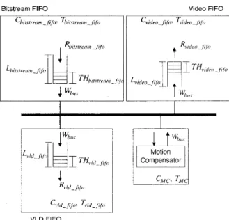
The bus and FIFO model for our MPEG-2 decoder is shown in Fig.
6.
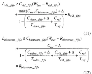
The Memory Controller consists of a non- preemptive fixed-priority scheduler to arbitrate the bus I/O. lower bound of the FIFO length associated with Video FIFO, VLD FIFO and Bitstream FIFO as:Lin, Chen, and Jen: Low Power Design for MPEG-2 Video Decoder 517
Rbitstrerrm- fifo
(12) The equations (lo), (1 1) and (12) shows that the FIFO length is determined by burst size of each transaction and the FIFO fillinglemptying rate of associated functional unit. The first term in equations (lo)-( 12) accounts for the FIFO capacity to sendheceive a burst of data to/from Memory Bus, while the capacity to accommodate the blocking by other tasks contributes the second one. Obviously, if the MPEG-2 decoder chip adopts fixed-priority scheme to arbitrate bus VO, data transfer may be blocked by another data transfer with the time proportional to the transfer burst size.
B. Bus Scheduling
and
Switching ActivityIn order to preserve the data correlation of VO transfers for image-type data, it is necessary to reduce the probability of intermixing the transactions of different VO processes on Memory Bus. As Fig. 7 is shown, transferring those I/O processes with larger burst size is a good way to reduce the intermixed probability and preserve the data correlation. However, equations (lo)-( 12) indicate that the internal buffer size should be increased in order to ensure that the FIFO will not be overflow or underflow and to prevent the functional units from starvation. Large internal buffer memories not only increase the chip area, but also consume more power. Therefore, in order to preserve the data correlation, the non-preemptive fixed-priority arbiter in Memory Controller must be modified to accommodate larger burst of memory access without affecting the size of the internal buffer.
Our goal is to construct a arbiter/scheduler to accommodate larger transaction length for different I/O processes without the necessity to increase the total FIFO size. We first analyze the characteristics of memory I/O transactions as listed in table 2. It can be found that the required bandwidth for the processes "Bitstream Read" and "Bitstream Write" are relatively lower. This means that the associated FIFO filling/emptying rates Rhrrvrrmrnfifi, and
Rv,c,Jifi, are also low and we can estimate the length of both FIFOs as:
and
-
Lbitsfreunz-fifn Chirsrreunz-
fife(
wbu.s - Rbitstreunz-fifo)(14) Therefore, we only have to find a strategy to reduce the extra length of Video
FIFO
to accommodate the blocking by low-priority tasks, which contribute the second term of equation (10).The data in table 2 also indicate that the transactions M C read, MC write and Video Read dominate the memory bus I/O time. However, because these
U 0
processes are deterministic, it is possible to schedule these tasks in the decoding time domain. According to the off-line schedule analyzed in advance, the Memory Controller then performs arbitration as follows. Normally, the Memory Controller monitors the I/O requests to o r from VBV buffer and performs the compressed bitstream transfer for VLD FIFO and bitstream FIFO. While it is time for U 0 process like Video Read, MC Read and MC Write, the bus will be allocated to that process until the transaction ends. The Memory Controller will then return to the state to handle the memory access to/from VLD FIFOhitstream FIFO. Because the processes Video Read, MC Read ad MC Write are off-line scheduled, the latter processes will not contribute the blocking time to the former.On
the other hand, the blocking time of Video Read contributed by process "Bitstream Read" and "Bitstream Write" will also be less because the scheduler polls the state of those FIFOs and fill/empty them as soon as possible. Therefore, by using the propose bus arbitration/scheduling scheme, we can estimate the length of Video FIFO as:Lvideo-,fifo 'video- j;fii(
Wbus
- Rvideo-fifo) (15)Compared to the fixed-priority scheme, the proposed scheme allows larger burst of memory access to Video FIFO. However, the required FIFO size will not be increased.
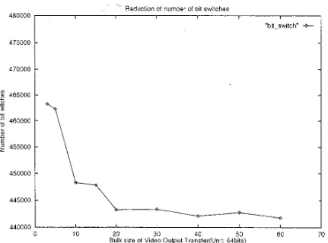
Fig. 7 shows that under the same FIFO size, the proposed bus scheduling scheme allows larger burst of memory access than the fixed-priority scheme. Table 3 shows the comparison of switching activity reduction by Gray code encoding scheme with different scheduling schemes for burst and FIFO sizing.
V. CONCLUSION
The wide connection between the MPEG-2 decoder and its associated frame buffer DRAM is used to provide sufficient I/O bandwidth. The large capacitances on this Memory Bus make the reduction of switching activity on the bus is needed in order to reduce the total power consumption of the whole decoding system. Because most image data that transferred on the bus are highly correlated in spatial domain, their transfer reveals highly temporal correlation. Using Gray code coding scheme to re-code the
518 IEEE Transactions on Consumer Electronics, Vol. 42, No. 3, AUGUST 1996
image data is then an effective way to reduce the bit switches on the Memory Bus because this code representation minimizes the Hamming distance for adjacent numbers. On the other hand, using large burst to transfer these image data may preserve more data correlation than using the shorter one. However, the total size of required I/O buffer is also larger while transferring data with large burst. A bus arbitration and scheduling scheme is then proposed to allow larger burst of
I/O
transfer with less buffer size penalty than the fixed-priority approach Both the Gray code representation and the proposed bus scheduling scheme are adopted in our MPEG-2 decoder VLSI to reduce the chip and system power dissipation.VI. ACKNOWLEDGE
This work is supported by the National Science Council under grant NSC 79-0414-E009-008 and United Microelectronics Corporation.
VII. REFERENCES
ISOiICE 13818, "Generic Coding of Moving Pictures and Associated," (MPEG-2).
Anantha P. Chandrakasan and Robert W. Brodersen, "Minimizing Power Consumption in Digital CMOS Circuits", Proc. of the IEEE, Vol. 83, No. 4, April 1995. Kiyoshi, et al., "A 600 mW Single Chip MPEGZ Video Decoder," IEICE Trans. on ELECTRON., Vol. E78-C, No.
12, Dec 1995.
E. Scopa, et al., "A 2D-DCT low-power architecture for H.261 coders," Proc. of ICASSP '95, P.3271-4, vol. 5, 1995
C-H. Lin, et. al., "The VLSI Design of MPEG2 Video Decoder," Proc. of International Conference on Computer Systems Technology f o r Industrial Applications '96. Tatsuhiko Demura, et. al., "A Single-Chip Video Decoder LSI," in Proc. ISSCC '94.
Mircea R. Stan, Wayne P. Burleson, "Bus-Invert Coding for Low-Power IiO", IEEE Trans. on VLSI System, Vol. 3, No. 1 , March 1995.
Ching-Long Su, Chi-Ying Tsui and Alvin M. Despain, "Saving Power in the Control Path of Embedded Processors," IEEE Design & Test Computers, Winter 1994. Daniel I. Katcher, Hiroshi Arkawa, and Jay K. Strosnider,
" Engineering and Analysis of Fixed Priority Scheduler,"
IEEE Trans. on Sofrwnre Engineering, Vol. 19, No. 9, September 1993.
Kevin A. Kettler and Jay K. Stosnider, "Scheduling Analysis of the Micro Channel Architecture for Multimedia Applications," Proc. of the International Conference on Multimedia Computing and Systems, 1994.
"RAM Buner Buffer
U2
video frame
0
pixel data
(a)video frame
0
pixel data
(b)Fig. 2 Data sequence for image data transfer, (a) I/O process
Lin, Chen, and Jen: Low Power Design for MPEG-2 Video Decoder Binary 6 Gravcode
---
519 &nary-
Gray code -+-Distribution 01 the next %bit dice value. MC Read
O O , , , , , , , , , , , , I , , , Toble Tennis 6 Football -t. Flower Garden 0 0 5 O 5
t
-', 3 5t
Distribution 01 the ne* &-bit slice va1ue:Video Read
07.51 , , , , , , , I , I , , , , , I Table Tennis +- Football -t- Flower Garden o
h
0 1 2 3 4 5 6 7 8 9 1 0 1 1 1 2 1 3 1 4 1 5 1 6 Value dinereme (b)Fig. 3. The distribution of bus value difference for the bit slice [N+8:N] on the Memory bus, (a) I/O process "MC Read", (b) I/O
process "Video Read".
0.3 0 2 0 1 0 0 1 2 3 4 5 6 7 8 9 l O 1 1 1 2 1 3 1 4 1 5 Value dineience
Fig. 4. The distribution of bus value difference for the bit slice [N+8:N+8-m] of the data (where N=O, 8, ..., 56 and m=4-8). The
I/O process is "MC Read".
O ~ " ~ ~ " " ~ ~ ~ ~ ' ~ 1 2 3 4 5 6 7 8 9 1 0 1 1 1 2 1 3 1 4 1 5 Value dlnerence (a) 1 2 3 4 5 6 7 8 9 1 0 1 1 1 2 1 3 1 4 1 5 Value diHwenc8 (b)
Fig. 5. The distribution of Hamming distance for binary code and Gray code, (a) 4-bit representation, (b) 8-bit representation.
--
,I.--
VLD FIFO
520
Video sequence
IEEE Transactions on Consumer Electronics, Vol. 42, No. 3, AUGUST 1996
Process Bit switches reduction Bit switches reduction Bit switches reduction (4-bit Gray code) @-bit Gray code) (Bus-Invert Coding,
one invert b for 8 b 480000 Table tennis Football Flower garden 475000 - MC Read 19% 22% 24% Video Read 17% 19% 23% MC Read 7 70 14% 10% Video Write 10% 13% 15% MC Read 6% 12% 13% Video Write 6% 10% 18% 470000 56 XORs 2 465000 3 5 460000 n $ 455000 128 XORs 450000
I
MOOOO (48 FAs) Reduction 01 number of bit sw8tchesMC Write /Deterministic Video Read IDetermnistic \
38 4M 15 2 M 15 2 M
10 20 30 40 50 GO
Bulk size of Video Output Transler(Unit 64blls)
Scheduling
Table Tennis Football Flower garden
Fig. 7. The relation between transfer bulk size and number of bit switches on the bus.
&bit Gray Code 8 bit Gray Code
Fixed-priority scheme The proposed Scheme Fixed-priority scheme The proposed Scheme
(Clit/ro=4, C,,,, = 16) (C!,t/e0=6, C,,,, = 3 2 ) (CLrdro=4, C,,,, = 1 6 ) (C,,d&, C,,,, = 32)
14% 26% 14% 27% 5 6% 18% 9 7% 23% 4 3% 17% 9 6% 21% 7000 GOO0 3 5000 2 o 4000 3 - m 3000 2000 1000 0 10 20 30 40 50 60
Bulk size 01 Video Output Transfer (Unn. 64bits)
Fig. 8. Relation between transfer bulk size and the size of internal buffer (Bitstream FIFO
+
VLD FIFO+
Video FIFO) in two schedulingiarbitration schemes; dot line: fixed-priority scheme, solid line: the proposed scheme.IImplementation
1
24XORslCoSt
64 latches
8 majority voters
Lin, Chen, and Jen: Low Power Design for MPEG-2 Video Decoder 521
ACM
Chia-Hsing Lin was born in Taipei, Taiwan, ROC, in 1969. He received the B.S. degree from National Chiao Tung University in 1991.
He is a Ph.D. Candidate in Electronics Engineering at EECS College of National Chiao Tung University, Hsinchu, Taiwan, ROC. His research interests include VLSI architecture for video signal processing, computer graphics and multimedia networking. He is a student member of IEEE and
Chen-Min Chen was born in Kaohsiung, Taiwan, ROC, in 1972. He received the B.S. and M.S. degrees from National Chiao Tung University, Hsinchu, Taiwan, in 1994 and 1996, respectively. His major research interests include low power analysis in software level of abstraction and embedded processor design. He is
a member of Phi Tau Phi.
Chein-Wei Jen was born in Shanghai, China, in 1948. He received the B.S. degree from National Chiao Tung University in 1970, the M.S. degree from Stanford University in 1977, and the Ph.D. from National Chiao Tung University in 1983.
He is a professor in the Department of Electronics Engineering and the Institute of Electronics, National Chiao Tung University, Hsinchu, Taiwan. From 1985 to 1986 he was a Visiting Researcher at the University of Southern California, USA. His current research interests include VLSI signal processing, VLSI architecture design, design automation, and fault tolerant computing. He is a member of IEEE and Phi Tau Phi.