國立交通大學
電 子 工 程 學 系 電 子 研 究 所 碩 士 班
碩 士 論 文
在電路延遲限制下降低晶片上匯流排功率消耗之
有彈性之匯流排編碼技術
Flexible On-chip Bus Encoding for Power Minimization under
Delay Constraints
研 究 生:林 子 為
指導教授:周 景 揚 博士
在電路延遲限制下降低晶片上匯流排功率消耗之
有彈性之匯流排編碼技術
Flexible On-chip Bus Encoding for Power Minimization
under Delay Constraints
研 究 生:林子為 Student: Tzu-Wei Lin
指導教授:周景揚 博士
Advisor: Dr. Jing-Yang Jou
國立交通大學
電子工程學系 電子研究所碩士班
碩士論文
A Thesis
Submitted to Department of Electronics Engineering & Institute of Electronics
College of Electrical Engineering and Computer Engineering
National Chiao Tung University in Partial Fulfillment of the Requirements
for the Degree of MASTER in
Electronics Engineering
2006
Hsinchu, Taiwan, Republic of China
在電路延遲限制下降低晶片上匯流排功率消耗之
有彈性之匯流排編碼技術
研究生:林子為 指導教授:周景揚 博士
國立交通大學
電子工程學系 電子研究所碩士班
摘要
隨著製程不斷之演進,在奈米製程下,如何有效地減少長導線之功 率消耗與電路延遲,已成為當前高效能晶片的設計難題,除此,奈米科 技下之電感性與電容性串音更進一步加深設計上之複雜度,尤其在干擾 導致電路延遲、串音雜訊與功率消耗上所造成之衝擊。導因於此,在文 獻中許多已提出之匯流排編碼之研究,在只考慮最差之電容性串音輸入 組態下,雖致力於減少電容之串音效應,以試圖同時減低功率消耗與電 路延遲(或只針對電路延遲或功率消耗做最佳化),但是,由於只考量電 容串音效應,產生之編碼結果,極有可能不適用於未來之高效能晶片, 尤其在電感效應明顯之晶片上。因此,在本篇論文中,我們提出一新式 之匯流排編碼技術,在使用者給定匯流排參數,工作時脈與電路延遲限 制後,此技術能同時考量電容、電感效應與延遲限制,做功率最佳化編 碼。最後,透過實驗結果證明,我們所提出之技術,再給定之延遲限制 下,確實可有效降低匯流排之串音造成延遲與功率消耗。Flexible On-chip Bus Encoding for Power Minimization
under Delay Constraints
Student:Tzu-Wei Lin Advisor:Dr.
Jing-Yang Jou
Department of Electronics Engineering & Institute of Electronics
National Chiao Tung University
Abstract
As technology advances, the global interconnect delay and the power consumption of long wires become crucial issues in nanometer technologies. In particular, both inductive and capacitive coupling effects between wires result in serious problems such as crosstalk delay, coupling noise, and power consumption. However, most existing works consider only RC effects (the worst-case switching pattern resulting from coupling capacitance) to develop their encoding schemes to reduce the bus delay and/or the bus power consumption. In this thesis, we propose a new bus encoding scheme for global bus design in nanometer technologies. With the user-given bus parameters, the working frequency, and the delay constraint, the scheme can minimize the bus power consumption subject to the delay constraint by effectively reducing the LC coupling effects. Simulation results show that the proposed scheme can significantly reduce the coupling delay and the power consumption of a bus according to the delay constraint.
誌謝
感謝周景揚老師無私的指導,以及對我的研究提出深入而獨到的見解使 得整個研究更有深度。而在老師的帶領下EDA 實驗室中和樂的氣氛以及在 學問上互相砥礪探討的氛圍幫助我學習到了做研究的方式及其精神,在學校 兩年的研究生涯,必然對我未來的發展與想法有著巨大的影響。 在實驗室成員中特別要感謝涂尚為學長,沒有他耐心的指導我的碩士論 文必然沒有如此的內涵。王承業學長在探討問題時的觀點與態度讓我深深的 佩服。石哲華學長、李耿維學長與吳孟臻學長在程式語言上及生活上的幫助 讓我在遇到困難時仍可以找出解決的方法。林亮宇學長豐富了我的人生的觀 點。江泰盈學長在我辛苦的碩一生涯給予的協助。李瑞梅學姊對於我生活上 的關懷。當然準博士生林步青與陳冠豪是我度過這兩年碩士生涯的最佳拍檔 謝謝他們。 我的爸媽,林繼志、嚴鳳珠,我的妹妹,林恆如,感謝他們在我學習過 程中的支持,他們的支持给我帶來最大的力量。最後我要感謝我的女朋友李 佳穎,有了他的陪伴是我的幸福。Contents
摘要... iii
Abstract ...iv
誌謝...v
Contents...vi
List of Tables ... viii
List of Figures ...ix
List of Figures ...ix
Chapter 1 Introduction ...1
1.1 Related Works on Bus Encoding...2
1.2 Our Approach ...3
1.3 Organization ...4
Chapter 2 Bus Encoding for Reducing Delay and Power...5
2.1 Preliminary ...5
2.1.1 Assumption and Problem Input...5
2.2 Bus Encoding Flow ...8
2.2.1 Overall Encoding Flow ...8
2.2.2 Extract RLC from Bus ...10
2.2.3 Simulate Basis Vectors by HSPICE... 11
2.2.5 Find Minimum Total Edge Weight b Clique ...15
Chapter 3 Simulation Results...33
3.1 Simulation Results of Delay and Power Reduction ...34
3.2 Delay and Power Reduction under Different Working Frequency..37
3.3 Power Minimization Only ...38
Chapter 4 Conclusions ...41
Reference...43
List of Tables
Table 1: The simulation results of the delay and power minimization for encoding 5-bit bus to 6-bit bus and 7-bit bus (↑: switching from “0” to “1”; ↓: switching from “1” to “0”; _: no switching) ...35
Table 2: The simulation results of the delay and power minimization for encoding 6-bit bus to 7-bit bus and 8-bit bus...35
Table 3: The simulation results of the delay and power minimization for n = 5 and m = 7 with the working frequency varying from 100MHz to 5GHz.
...37
Table 4: the simulation result of the power minimization only for n = 5~6 and m = 6~8...38
List of Figures
Figure 1: The coplanar bus structure...6
Figure 2: The overall bus structure including the encoder and decoder...7
Figure 3: The overall encoding flow. ...9
Figure 4: Extract RLC and generate the corresponding SPICE file. ...10
Figure 5: HSPICE simulations with the minimum basis vectors of the minimum basis vector set. ...13
Figure 6: An example of superposition. ...15
Figure 7: Proposed flow for finding the valid code set. ...17
Figure 8: An example of SOM, SN and C...18
Figure 9: Flow of the 1-opt Local Search. ...19
Figure 10: Flow of MLS...21
Figure 11: Pseudo code of the Modified Local Search for finding minimum total edge weight b clique...23
Figure 12: A 10-node transition graph...25
Figure 13: The seed node “3” is chosen at Step 1 in Figure 7, and S0N is generated. (The current clique ={3}.)...26
Figure 14: A candidate node “4” with minimum average edge weight is chosen and added to the current clique at Step 2 in Figure 7. (The current clique = {3, 4}.)...27
Figure 15: A candidate node “2” with minimum average edge weight is chosen and added to the current clique at Step 2 in Figure 7. (The current
clique = {2, 3, 4}.)...28
Figure 16: Node “2” with the fewest connection to S3OM is chosen and dropped from the current clique at Step 3 in Figure 7. (The current clique = {3, 4}.)...29
Figure 17: Node “5” with the minimum average edge weight in S4N is chosen and added to the current clique at Step 3 in Figure 7. (The current clique = {3, 4, 5}.)...30
Figure 18: Node “6” with the minimum average edge weight in S5N is chosen and added to the current clique at Step 3 in Figure 7. (The current clique = {3, 4, 5, 6}.)...31
Figure 19: Final result after MLS...31
Figure 20: The simulation results of n = 5 and m = 6 ~ 10 for...39
Chapter 1
Introduction
As technology advances into nanometer technology era, the delay and power consumption become two critical problems in the on-chip bus design. With aggressive scaling of transistor gate lengths, the bus delay and the power dissipation of the bus wire loads play important roles in the overall performance of high-speed chips. Besides, due to the lower supply voltage (lower noise margin) and more congested interconnects, the crosstalk problem resulting from both inductive and capacitive coupling effects becomes another important issue in deep-submicron designs [1]. Hence, the strong coupling effects between wires make the delay and the power consumption of on-chip buses worse than before. Therefore, it is crucial to reduce the delay and power consumption of the on-chip bus to improve the circuit performance in DSM designs.
1.1 Related Works on Bus Encoding
Due to the higher wire aspect ratio and smaller wire pitch, the coupling capacitance between neighboring wires becomes the dominant component of the total wire capacitance. Moreover, when the clock frequency increases over GHz, the inductance effects on on-chip interconnects are becoming increasingly significant [1]. However, most existing works focus on reducing the effects resulting from coupling capacitance on the bus structure. There is not much work in the literature considering inductance effects on the bus structure to develop encoding schemes for reducing the bus delay and power consumption. Considering only the capacitive coupling effect, Sridhara et al. [2], Sotiriadis and Chandrakasan [3], Victor and Keutzer [4], Baek et al. [5], and Hirose and Yasurra [6] proposed their bus encoding techniques to eliminate the crosstalk delay. They try to avoid the simultaneous inverse transitions of neighboring wires. Based on eliminating the same worst capacitive coupling patterns, Baek et al. [5], Shin et al. [7], Zhang et al. [8], Sridhara et al. [9], Subrahmanya et al.[10], Lindkvist et al. [11], and Sotiriadis et al. [12] develop their own bus encoding scheme to reduce the bus power consumption.
Since most previous encoding schemes [2 − 12] optimize the bus delay and/or power consumption considering only the capacitive coupling, they might not be suitable for today’s high-performance on-chip bus design due to the significant inductive coupling. Although some works [13, 14, 15] consider the inductance effects to build their encoding schemes, they either neglect the capacitive coupling effects or only reduce the bus delay. However, as pointed out
in [16], the worst-case pattern causing the largest transition delay varies with given design parameters while consider the RLC effects on buses. Besides, the power consumption is also a crucial problem in the bus design. Therefore, when developing an encoding scheme for high performance buses, the given parameters need to be considered to minimize the bus power consumption and the coupling delay.
1.2 Our Approach
As the process technology advances and the clock frequency increases over GHz, the inductance effects on on-chip interconnect structures have become increasingly significant [1]. Most existing works focus on reducing the effect resulting from the coupling capacitance on the bus structure. There is not much work in the literature considering the inductance effects on the bus structure to develop encoding schemes to reduce the bus delay. However, considering the
RLC circuit model for the bus structure, we found out that when the inductance
effect dominates, the worst-case switching pattern with the largest on-chip bus delay is when all wires simultaneously switch in the same direction [16]. Furthermore, in [16], the authors indicate that while considering the RLC effect of interconnects, the worst-case switching pattern will change under different levels of interconnect (local, medium, or global wire) and different working frequency. Hence, as the inductance cannot be neglected in today’s high-performance circuit design, it is very important to consider the RLC effect
while developing the bus encoding schemes. From [16] and the previous discussions, we can understand that the impacts caused by aggressors are very diverse through the mixture of the capacitive and inductive coupling. Therefore, the worst-case delay patterns could be very different for various bus wire parameters, i.e., different inductive and capacitive coupling conditions. Moreover, the capacitive and inductive coupling effects vary with different working frequencies since the impedance of capacitance (jωC)-1 (where ω = 2πf)
decreases with the frequency but the impedance of inductance jωL increases.
Therefore, when considering RLC effects, it is crucial to take design parameters into account to derive a better bus encoding scheme.
Thus, with the concept that the worst-case switching pattern varies with given design parameters while consider the RLC effect of interconnects, we propose a flexible encoding scheme for on-chip buses with given parameters. The key idea is that the coupling effect should be alleviated by transforming the data sequences transmitting through on-chip buses.
1.3 Organization
The rest of this thesis is organized as follows. Section 2 describes the basic assumptions used in our work for the bus structure, and this section also details our encoding flow and algorithm that is used to minimize the LC coupling effects. Simulation results are shown in Section 3. Finally, Section 4 concludes the thesis.
Chapter 2
Bus Encoding for Reducing Delay
and Power
2.1 Preliminary
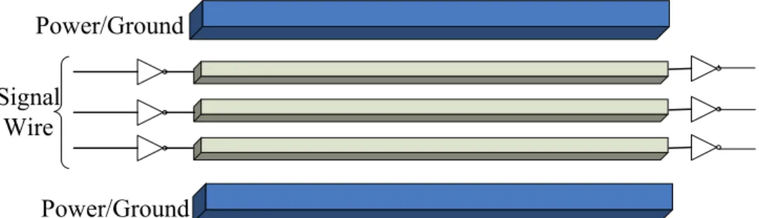
Signal Wire
Power/Ground
Power/Ground
Figure 1: The coplanar bus structure.
In this thesis, we consider the coplanar bus structure as shown in Figure 1 to build our encoding scheme. In the coplanar bus structure, we assume that each driver (receiver) has a uniform size and the driver is also assumed to be symmetric so the effective output resistance is the same for both rising and falling signal transitions. In the bus structure, each signal wire has a uniform width, pitch, length and height. Given the parameters of wires (length, width, height and pitch), delay constraint, working frequency, and the number of data bit
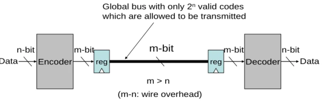
n, we will generate a valid code set that has the minimal total transition power to map the data patterns. The valid code set is obtained at the cost of m – n
extra bus wires. Any valid code set must satisfy the property that any transition between codes within this set is guaranteed to meet the delay constraint. The overall bus structure is shown in Figure 2. The valid code set of the global bus contains only 2n out of 2m possible codes. The mapping between the data patterns
and the generated code set is a straight forward work and will not be discussed in this thesis.
Encoder Decoder Data
n-bit m-bit
m > n
Global bus with only 2nvalid codes which are allowed to be transmitted
(m-n: wire overhead) reg m-bit Data n-bit reg m-bit
Figure 2: The overall bus structure including the encoder and decoder.
Assume the number of data bit is n, the overall bus structure is shown in
Figure 2. The valid code set of the global bus contains only 2n out of 2m possible
codes. The specific 2n codes are selected to minimize the coupling effects
between any two of them. In addition, the transition delay between any two patterns in the specific 2n codes will meet the delay constraint which is given by
users.
Since transistors mainly operate in the linear region during transitions, it is assumed that all drivers’ output resistances are linear throughout the simulations. Therefore, the drivers will be modeled as simple linear resistances. In addition, the receivers will be replaced by equivalent gate capacitances in the circuit model and the wires are replaced by equivalent RLC circuit models. With the models, the built circuit model for the coplanar bus structure will be constructed by only linear elements (linear R, L, and C). In other words, the built circuit is a LTI (linear time invariant) system.
transition time τr can be calculated from the working frequency f by the following equation [17]: (1) 35 . 0 • = f r τ
In our simulation, we assume that synchronous registers are located at the transmitter side. Thus all the signals switch at the same time on the bus.
2.2 Bus Encoding Flow
2.2.1
Overall Encoding Flow
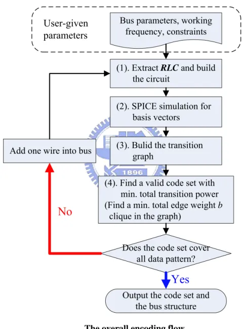
Figure 3 illustrates our overall encoding flow. At first, users should give the
bus parameters (bus width n, wire dimensions, wire pitch, Power/Ground grid dimensions, Power/Ground-to-signal pitch), the working frequency, and the delay constraint. With the given parameters, we extract the resistances, capacitances, and inductances of bus wires. After extraction, the equivalent RLC circuit will be built. Next, the built circuit will be simulated by using HSPICE with the basis
vectors which will be defined later. By applying superposition theorem [18] of
linear circuits, we can establish the transition graph efficiently. From the transition graph, we apply a modified local search algorithm [19] to find a valid code set in which every transition between a code pair meets the delay constraint
and the total transition power of all code pairs is minimized. Next, we will check whether the code set covers all data patterns. If not, we add one more bit line to the bus structure and redo from Step (1). Otherwise, the code set will be output to map to the data patterns with the corresponding bus structure. The details of each step will be described in the following subsection.
Bus parameters, working frequency, constraints
User-given parameters
(1). Extract RLC and build the circuit
(2). SPICE simulation for basis vectors
(3). Bulid the transition graph
(4). Find a valid code set with min. total transition power (Find a min. total edge weight b clique in the graph)
Does the code set cover all data pattern?
Output the code set and the bus structure Add one wire into bus
Yes
No
Figure 3: The overall encoding flow.
2.2.2
Extract
RLC from Bus
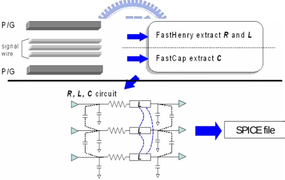
In step (1), with the given feasible parameters, FastCap [20] and FastHenry [21] are used to extract the RLC parameters of the bus and construct the SPICE model. The detailed flow of step (1) is shown in Figure 4. FastCap can extract the self and coupling capacitance of wires, while FastHenry is developed to extract the resistance, self inductance, and coupling inductance. With these extracted RLC parameters, the equivalent RLC circuit models will be constructed. The circuit models are constructed as π-segments using series resistances and inductances and shunt capacitances. The circuit model will be outputted as a SPICE file.
SPICE file
SPICE file
2.2.3
Simulate
Basis Vectors by HSPICE
After building the RLC circuit model, the transition delay and power for a specific input pattern pair can be obtained by simply conducting HSPICE simulation. However, for an n-bit bus, there are 2n input patterns and 4n possible
transition patterns in total. It is extremely time-consuming to simulate all transition patterns by HSPICE when n goes higher. The time complexity is 4n*(HSPICE simulation time for a transition pattern). Hence, we develop a
method based on superposition theorem [18] to significantly reduce the simulation time. Based on this idea, we first simulate the basis vectors which are independent sources to the RLC circuit. Then the real delay of each transition pattern can be obtained by superposing the simulation results of the basis vectors.
What are the basis vectors for a bus? We define them as all independent transitions of bus inputs. Throughout this thesis, “–” represents a stable input (stable at low or high), “↑” represents an input changing from low to high, and “↓” represents an input changing from high to low. Therefore, for an n-bit bus consisting of input signals z0 , z1 , z2 ,…,zn-1 , the basis vectors can be expressed
as:
basis vectors of an n-bit bus =
{(z0 z1 z2 …zn-1 )| z0 ∈{↑, ↓} and z1 , z2 ,…zn-1 ∈{–}}∪
{(z0 z1 z2 …zn-1 )| z1 ∈{↑, ↓} and z0 , z2 ,…zn-1 ∈{–}}∪
• •
The followings are some properties of the basis vectors.
Property 1: In an linear RLC circuit of a bus, given a basis vector, such as (– –
↑), the transition delay and power due to the switching input is the same no matter other stable inputs are at ‘0’ or ‘1’ [15] (e.g. 000Æ001 and 110Æ111 have the same transition delay).
Property 2: In an linear RLC circuit of a bus, given an integer k and
,{( z 1
0≤k≤n− 0 z1 z2 …zn-1 )| zk ∈{↑} and z0 , z1 ,…zn-1 ∈{–}} and {( z0 z1 z2
…zn-1 )| zk ∈{↓} and z0 , z1 ,…zn-1 ∈{–}} are called a dual basis vector pair. The
voltage and current waveforms resulting from a dual basis vector pair are equal in magnitude but opposite in direction [15].
Here we also define a minimum basis vector set as that all transition patterns can be obtained by superposing the basis vectors within this set:
Minimum basis vector sets of an n-bit bus =
{{(z0 z1 z2 …zn-1 )| z0 ∈{↑, ↓} and z1 , z2 ,…zn-1 ∈{–}},
{(z0 z1 z2 …zn-1 )| z1 ∈{↑, ↓} and z0 , z2 ,…zn-1 ∈{–}},
•
•
Therefore, the minimum basis vector set of an n-bit bus has n elements and each element can be one of the dual basis vector pairs as shown in Equation (3). Hence, we only need to simulate the basis vectors of the chosen minimum basis
vector set. Then we can use the simulation results to obtain the delay and power
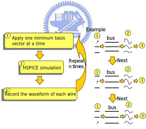
of all transition patterns by applying the superposition theorem. The details and examples of Step (2) are shown in Figure 5. First, we apply one basis vector at a time as the input transition pattern on the bus. Second, we perform SPICE simulation and record the voltage and current waveforms of all signal wires. Then, we repeat this procedure for every basis vector until all basis vectors of the chosen minimum basis vector set are simulated.
Record the waveform of each wire
Record the waveform of each wire 3
Record the waveform of each wire
3
HSPICE simulationHSPICE simulation Apply one input source at one timeApply one input source at one time
1
2
HSPICE simulationHSPICE simulation Apply one input source at one timeApply one minimum basis vector at a time
1
2
Record the waveform of each wire
Repeat n times
Record the waveform of each wire
Record the waveform of each wire 3
Record the waveform of each wire
3
Record the waveform of each wire
Record the waveform of each wire 3
Record the waveform of each wire
3
HSPICE simulationHSPICE simulation Apply one input source at one timeApply one input source at one time
1
2
HSPICE simulationHSPICE simulation Apply one input source at one timeApply one minimum basis vector at a time
1
2
Record the waveform of each wire
Repeat n times Example ↑ 3 1 2 ↑ 3 1 2 ↑ 3 1 bus 2 3 1 2 Next bus Next 3 2 3 2 bus 1 1 Example ↑ 3 1 2 ↑ 3 1 2 ↑ 3 1 bus 2 3 1 2 Next bus Next 3 2 3 2 bus 1 1
Figure 5: HSPICE simulations with the minimum basis vectors of the
2.2.4
Build
Transition
Graph
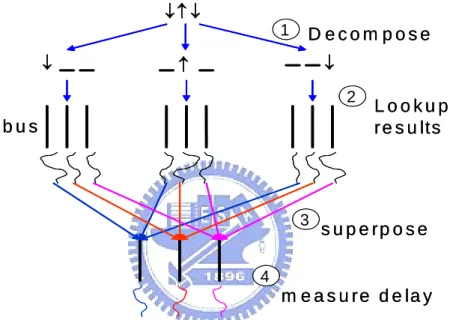
In step (3), we apply the superposition theorem to calculate the real transition delay of each transition pattern by using the simulation results of the
basis vectors in step (2). Figure 6 illustrates how to obtain the real delay of a
transition pattern by using the simulation results of the basis vectors. First, we decompose the transition pattern into some basis vectors. Then, by looking up the simulation results of the basis vectors that have been obtained in step (2) and superposing them, we can obtain the overall voltage waveform of each wire. Then the real delay of this transition pattern can be calculated. Our simulation results show that the results obtained from superposition exactly comply with those obtained from the real HSPICE simulation.
By using superposition, the overall current waveform of each wire can be obtained as well. Then the transition power between any two codes can be obtained from the following equation:
(4)
∑
=⋅
=
n i i ddI
V
P
1 avgpower
Transition
where Ii avg is the average current in wire i.
Hence, by utilizing the superposition, we can calculate the transition delay and power between any two codes very fast without performing a real HSPICE simulation run. Then we build a transition graph to indicate if the transition delay between arbitrary two codes meets the delay constraint or not and record the
transition power as the edge weight. In the transition graph, a node represents a code and an undirected weighted edge indicates that the transition delay between two corresponding codes meets the delay constraint with the transition power as the edge weight.
1 ↓ ↑ ↓ ↓ ↑ ↓ D e c o m p o s e L o o k u p r e s u lts 2 3 b u s s u p e r p o s e 4 m e a s u r e d e la y 1 ↓ ↑ ↓ ↓ ↑ ↓ D e c o m p o s e L o o k u p r e s u lts 2 3 b u s s u p e r p o s e 4 m e a s u r e d e la y
Figure 6: An example of superposition.
2.2.5
Find Minimum Total Edge Weight b Clique
2.2.5.1
Our Proposed Flow for Finding Valid Code Set
After building the transition graph, we want to find a minimum total edge weight b (=2n) clique in the graph. The reasons to find such a clique in the
transition graph are: (a) we want to find a valid code set that can map to all data patterns, i.e., the size of the valid code set equal to 2n data patterns; (b) within the
valid code set, any transition between two codes is guaranteed to meet the delay constraint; (c) the total transition power of this code set can be minimized, and thus the average power consumption of the encoded bus can also be minimized.
Inspired by the K-opt Local Search [19], we propose Modified Local Search
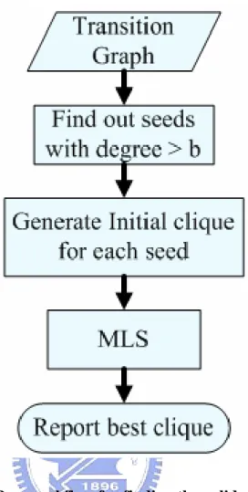
(MLS) to solve the problem. In Figure 7, we propose a flow for finding the valid
code set. Since finding the maximum clique is an NP-complete problem, the
K-opt Local Search is a heuristic algorithm. The algorithm can process the graph
up to 4000 nodes. Therefore, the proposed Modified Local Search is also a heuristic algorithm. By applying the Modified Local Search, the quality of the finding valid code ser would be improved both on the size and the total edge weight of the finding clique.
As shown in Figure 7, given a weighted transition graph, our goal is to find out a valid code set that can map to all the data patterns with minimum total edge weight (i.e. minimum total transition power). There are three steps in our proposed flow. First step is finding out the seeds with degree larger than b. The next is generating the initial clique for each seed. The third step is processing each clique by MLS.
Figure 7: Proposed flow for finding the valid code set.
2.2.5.2
Notations
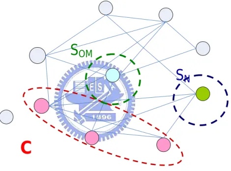
The notations used in this thesis are given below. An example is given in
Figure 8 to demonstrate the notations.
C
: the current clique.S
N: the neighbor node set in which the node can be added to enlarge C,i.e., the vertices are connected to all vertices of C. For example, SN = {8} in
S
OM: the node set of one edge missing, i.e., the vertices that areconnected to |C| − 1 vertices of C. For example, SOM = {5} in Figure 8.
Ci, SiN , SiOM: the current clique, the neighbor node set, and the node set of
one edge missing in iteration i, respectively.
Total-Power(C): the sum of all edge weights of C.
Figure 8: An example of SOM, SN and C.
2.2.5.3
Finding Seeds and Generating Initial Cliques
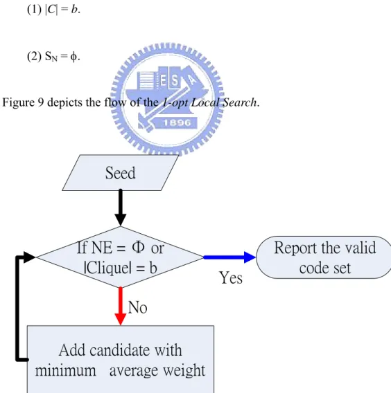
After the weighted transition graph is built, we use the 1-opt Local Search [19] to develop initial cliques from seeds. Due to the size of our target clique is b, the edge degree of seeds should be larger than b.
Since initial cliques are inputs of MLS, the performance of MLS will depend
S
NS
OMon the given initial cliques. Hence, different initial cliques should be tried by
MLS as many as possible to find the global optimum. To generate initial cliques,
we apply the 1-opt Local Search to develop them from seeds. Given a graph, nodes with edge degree larger than b will be chosen as seeds. Once a seed is chosen, the corresponding initial SN and SOM will also be generated. To enlarge a
clique, we choose a candidate from SN at a time. The candidate is the node with
the minimum average weight. After adding the candidate into the clique, SN and
SOM will be updated. The procedure continues until two conditions are satisfied:
(1) |C| = b.
(2) SN = φ.
Figure 9 depicts the flow of the 1-opt Local Search.
If NE = Φ or
|Clique| = b
Add candidate with
minimum average weight
Yes
No
Seed
Report the valid
code set
2.2.5.4
Modified Local Search
Inspired by the k-opt Local Search [19], we propose Modified Local Search to solve the problem in this thesis.
As described in the following, there are two basic ideas of the algorithm. Given a current clique C for a graph G:
(i). If |C| < b, by dropping a node set A contained in C, we can add a different node set B contained in current SN (|B| > |A| and assume B is also a clique)
of the resulting clique C − A. Then the resulting larger clique size |C| − |A| + |B| can be obtained.
(ii). If |C| = b, by dropping a node set A contained in C, we can add a different node set B contained in current SN (|B| = |A|, assume B is also a clique and
Total-Power(B) < Total-Power(A)) of the resulting clique C − A. Then a new clique (C − A) ∪ B will have the same size with C but smaller total edge weight than C.
According to the two ideas, we give a flow as shown in Figure 10 to detail MLS.
Transition
graph and
initial clique
Initialization
If S
N= F or
|C| = b
Add Phase
Is every node in initial
clique tried?
Is better clique found?
Yes
No
Report the valid
code set
No
Yes
NO
Yes
Drop Phase
Figure 10: Flow of MLS.
The procedures of Modified Local Search are given as follows. Given a initial clique C0 (| C0|< b) with S
N0 ≠ φ, the first solution C1 can be obtained by C0 ∪ {v},
is update to be SN1 and S1OM, respectively. The adding procedure is repeated until
SN = φ or |C| = b.
After some adding procedures are performed (assume α times), either the condition “SαN = φ” or “|Cα| = b” will be encountered. If “SαN = φ” is
encountered, our algorithm tries to find larger cliques after dropping one or several vertices from Cα. Otherwise, if “|Cα| = b” is encountered, the Modified
Local Search will try to find a better b clique with smaller edge weight after
dropping one or several vertices from Cα.
The dropping procedure begins when either the condition “SαN = φ” or “|Cα| =
b” is encountered. This procedure is continued until no node can be dropped from
the current clique, or one or some vertices can be added during adding phase (i.e., Sα+βN ≠ φ after performing β times dropping). During the dropping procedure, a
node v ∈ Cα that can result the largest Sα+1N is chosen. Hence, when the next
adding procedure is performed, many candidates can be chosen from SNα+1 and
added to Cα+1. The node v ∈ Cα that results the largest Sα+1Ncan be found by
checking all vertices of Cα and choosing the one with most lacking edges to v in
SαOM.
The adding and dropping procedure will be repeated until a termination condition is satisfied. The information of SN and SOM will be updated whenever a
node is added or dropped.
When the termination condition is encountered after p iterations, we choose the best one Cx from C1 to Cp (1 ≤ x ≤ p). The “best” Cx could be either the
“largest” clique among C1 to Cp when all cliques’ size is smaller than b or Cx
could be the clique with “minimum” total edge weight when some cliques’ size is equal to b. Then the best solution becomes a new initial clique C0 := Cx for the
next search. The Modified Local Search is continued until no better solution is found.
Figure 11: Pseudo code of the Modified Local Search for finding minimum total edge weight b clique.
Figure 11 shows the pseudo code of the Modified Local Search for the
minimum total edge weight b clique problem. In our pseudo code, two variables
g and gpower (lines 2 and 3) are used to denote the clique size gain and the
minimum total edge weight in each iteration. A candidate set PO (line 2) is used to prevent the cycling among the solutions. Only one node in PO can be added or dropped in each iteration.
The Modified Local Search has inner and outer loops. In the inner loop (lines 4 to 25), given a initial solution, several adding and dropping procedures are performed with the restriction of PO, and the best solution is chosen. In the outer loop (lines 1 to 29), the chosen best solution will be checked if it is better than the previous one (Cpre) by comparing with gmax and gpower (lines 26 and 27). The
maximum gain gmax is updated in the adding procedure (line 11). gmax is the
difference between the current best solution and Cpre at line 2. On the other hand,
the minimum total edge weight gpower is also updated in the adding procedure
(line 13). gpower keeps recording the minimum total edge weight in the inner loop.
The termination condition of the inner loop (line 25) is “DR = φ“. Initially,
DR is set to the initial clique Cpre at line 2 before entering the inner loop. When a
node v is dropped in the dropping procedure, it is deleted from DR if v is contained in Cpre at line 23.
2.2.5.5
Example
To demonstrate how the MLS works, we use an example as shown in
Figures 12-19 to go through our algorithm. Given a 10-node graph in Figure 12,
we want to find a clique with size 4 (b = 4). First, the 1-opt Local Search is conducted to find an initial clique (Figures 13-15). Next, the initial clique is input to the MLS to find a “better” clique (In this example, we first try to find a larger clique, and then we try to minimize the total edge weight of the clique.) (Figures 16-19).
In Figures 12 -19, the shaded number beside the node represents the average edge weight of the node.
6 4 8 7 3 9 1 2 8 1 3 10 5 5 2 3 3 1 4 2 3 7 4 7 1 4 5 8
2.25
4.3
4
5.7
6.5
4.5
3.2
2.3
3.6
0
(I). At Step 1 in Figure 7: As illustrated in Figure 13, we choose the seed node “3” with degree is 4 and average edge weight 3.2. Then there will be 5 candidates in S0N. 6 4 8 7 3 9 10 5 2 1
2.25
4.3
4
5.7
6.5
4.5
3.2
2.3
3.6
0
S
0NC
0Figure 13: The seed node “3” is chosen at Step 1 in Figure 7, and S0N is
generated. (The current clique ={3}.)
(II). At Step 2 in Figure 7: As shown in Figure 14, we choose the node “4” with the minimum average weight and add to the current clique. Therefore, the clique is {3, 4}, and S1N is {2,5,6}.
6 4 8 7 3 9 10 5 2 1
2.25
4.3
4
5.7
6.5
4.5
3.2
2.3
3.6
0
S
1NC
1Figure 14: A candidate node “4” with minimum average edge weight is chosen and added to the current clique at Step 2 in Figure 7. (The current clique = {3, 4}.)
(III). At Step 2 in Figure 7: As shown in Figure 15, we extend the current clique with the only candidate node “2”. S2N is updated to φ. Since the
termination condition of 1-opt Local Search is satisfied, the clique {2, 3, 4} is outputted as an initial clique.
C
2S
2OM 6 4 8 7 3 9 10 5 2 12.25
4.3
4
5.7
6.5
4.5
3.2
2.3
3.6
0
Figure 15: A candidate node “2” with minimum average edge weight is chosen and added to the current clique at Step 2 in Figure 7. (The current clique = {2, 3, 4}.)
(IV). At Step 3 in Figure 7: Since S2N = φ, no node can be added to the current
clique. Hence, in MLS, we will drop the node with the fewest connections to SOM.
As illustrated in Figure 16, node “2” has no connection to S3OM, and thus it is
S
3OM 6 4 8 7 3 9 10 5 2 12.25
4.3
4
5.7
6.5
4.5
3.2
2.3
3.6
0
C
3Figure 16: Node “2” with the fewest connection to S3OM is chosen and
dropped from the current clique at Step 3 in Figure 7. (The current clique = {3, 4}.)
(V). At Step 3 in Figure 7: As shown in Figure 17, 2 nodes is added back to S4N after dropping the node “2”. Again, we choose the node with minimum
average weight in S4N. Now, node “5” is chosen and added in the current clique,
S
4N 6 4 8 7 3 9 10 5 2 12.25
4.3
4
5.7
6.5
4.5
3.2
2.3
3.6
0
C
4Figure 17: Node “5” with the minimum average edge weight in S4N is
chosen and added to the current clique at Step 3 in Figure 7. (The current clique = {3, 4, 5}.)
(VI). At Step 3 in Figure 7: As shown in Figure 18, there is only one node in S5N that can be added. Therefore, we obtain a clique with size 4 which is larger
6 4 8 7 3 9 10 5 2 1
2.25
4.3
4
5.7
6.5
4.5
3.2
2.3
3.6
0
S
5NC
5S
5OMFigure 18: Node “6” with the minimum average edge weight in S5N is
chosen and added to the current clique at Step 3 in Figure 7. (The current clique = {3, 4, 5, 6}.)
(VII). At Step 3 in Figure 7: As shown in Figure 19, since the size of the current clique C6 is larger than the size of the initial clique C3, our next step is try to minimize the total edge weight gpower.
6 4 8 7 3 9 10 5 2 1
2.25
4.3
4
5.7
6.5
4.5
3.2
2.3
3.6
0
C
6From (IV) – (VII), although we obtain a larger clique, the MLS continues optimizing the clique. The clique found at (VI) will be set as a new initial clique to MLS, and the MLS will restart. In this example, the clique found at (VI) is optimal. Therefore, the following steps of the flow are not shown for short.
However, in order to find the global optimum, we must try as many seeds as possible in our flow.
Chapter 3
Simulation Results
In this chapter, we first show the simulation results of utilizing our encoding scheme to reduce the power consumption of the on-chip bus subject to the delay constraint, and then the results of power optimization only by using our encoding scheme are also given to demonstrate the efficiency of our work.
In our encoding flow, we iteratively applied the Modified Local Search with different initial cliques after building the transition graph. Finally, the best clique will be chosen and outputted as the final result. The initial cliques are generated by iteratively executing the modified 1-opt Local Search with different single node as a seed. Therefore, if there are q vertices with edge degree larger than b in a graph G, the modified 1-opt Local Search will be executed q times and total q
initial cliques will be generated. By utilizing the initial cliques, our flow can find a global optimum solution rather than a local solution.
To demonstrate the efficiency of our approach, we implemented the encoding flow in C++ and applied with the same setting in [15].
3.1 Simulation Results of Delay and Power Reduction
In the following simulations, the length, width, height, pitch of signal wires, and Power/Ground-to-signal pitch are 2000μm, 2μm, 2μm, 4μm, and 13μm, respectively. The bus working frequency is 1GHz and the supply voltage is 1.2V. The delay constraint is set to 300ps and the coupling to self capacitance ratio is 5.
Table 1 shows the simulation results of a 5-bit bus with wire overheads (m − n)
varying from 1 to 2, while Table 2 lists the results of a 6-bit bus. In Tables 1 and
2, column 2 shows the simulation results of the original bus without encoding.
Columns 3 and 5 list the simulation results of previous work [15] which are only encoded bus to meet the delay constraint without power minimization (denoted as “[15]”). The simulation results of the encoded buses with power minimization in this work (denoted as “Ours”) are shown in columns 4 and 6. Dworst denotes the
worst-case switching delay of the bus, while ΔPpeak and ΔPavg denote the peak
and average power saving, respectively. Patworst_D and Patworst_P represent the
worst-case switching patterns for the bus delay and power consumption, respectively.
Table 1: The simulation results of the delay and power minimization for encoding 5-bit bus to 6-bit bus and 7-bit bus (↑: switching from “0” to “1”; ↓: switching from “1” to “0”; _: no switching)
Table 2: The simulation results of the delay and power minimization for encoding 6-bit bus to 7-bit bus and 8-bit bus
As shown in Tables 1 and 2, the worst-case switching delays of the original buses do not satisfy the delay constraint (300ps). However, after applying our bus encoding scheme, all the worst-case switching delays of the encoded buses are less than the delay constraint. As shown in Row 2, since the switching patterns resulting in the worst-case delay are eliminated by our encoding scheme, the
worst-case bus delay can be minimized to meet the delay constraint. From Tables
1 and 2, we observe that the average power consumptions of the encoded buses
of previous work [15] could be worse than those of the original buses, although the peak power saving can be up to 25%. However, when the buses encoded both for delay and power minimization in this work, the average and peak power saving can be up to 16% and 44%, respectively, with one wire overhead (m − n = 1). For two wire overheads, the average and peak power saving can be up to 21% and 53%, respectively. In these simulations, we can also observe that there is only a slight or even no difference between the worst-case delay and power pattern as shown in column 2 of Tables 1 and 2. This is because the capacitance effect is the dominant factor in these simulations.
3.2 Delay and Power Reduction under Different
Working Frequency
Table 3: The simulation results of the delay and power minimization for n = 5 and m = 7 with the working frequency varying from 100MHz to 5GHz.
In this section, we will show the flexibility of our encoding flow for various working frequencies. We vary the bus working frequency from 100MHz to 5GHz and list the simulation results in Table 3. The same wire parameter and supply voltage are applied. The coupling to self capacitance ratio is set to 2.5. From
Table 3, we can observe that the worst-case delay pattern changes from the
capacitance-dominated one to the inductance-dominated one as the working frequency increases. Thus the efficiency of the power optimization of our encoding scheme tends to decrease as the frequency increases. This is because when the inductance effect becomes more significant than the capacitance effect, the worst-case delay pattern changes to the inductance-dominated one, but the worst-case power pattern is still the capacitance-dominated one.
3.3 Power Minimization Only
In this section, we utilize our encoding scheme to optimize the bus power consumption only by loosening the delay constraint. The wire parameters and supply voltage are the same with the previous section. The working frequency is set to 1GHz and the coupling to self capacitance ratio is 5. The simulation results are listed in Table 4. As shown in Table 4, when optimizing the bus power consumption only, the average and peak power saving can be up to 17% and 43%, respectively, with one wire overhead. For two wire overheads, the average and peak power saving can be up to 22% and 50%, respectively. In addition, the worst-case delay can also gain a little improvement.
m = 5 m = 6 m = 7 m = 6 m = 7 m = 8
Dworst (ps) 329 328 315 338 330 321
ٛPavg (%) 0 17.78 19.82 0 14.78 22.07
ٛPpeak (%) 0 43.84 44.7 0 36.37 50.8
Scheme n = 5 n = 6
Table 4: the simulation result of the power minimization only for n = 5~6 and m = 6~8.
14% 16% 18% 20% 22% 24% 26% m = 6 m = 7 m = 8 m = 9 m = 10
average power saving
(a) 10% 20% 30% 40% 50% 60% 70% m = 6 m = 7 m = 8 m = 9 m = 10
peak power saving
(b)
Figure 20: The simulation results of n = 5 and m = 6 ~ 10 for (a) average power saving and (b) peak power saving.
With the same wire parameters and working frequency, we vary wire overheads from 1 to 5 with n = 5 and the simulation results are shown in Figure
20. From Figure 20, we observe that although the peak power saving does not
the wire overhead increases. This is due to the fact that as the wire overhead increases, there are more codes could be used to optimize the power consumption than that with less wire overhead. In addition, since we are always eager to minimize the average power, the peak power saving may not always be maximized.
Chapter 4
Conclusions
In this work, we propose a flexible on-chip bus encoding flow considering bus parameters to minimize the bus power consumption subject to the delay constraint by effectively reducing the LC coupling effects.
To improve the quality of the finding valid code set, we proposed the
Modified Local Search to solve the minimum total edge weight b clique problem
in this work. Simulation results show that our encoding method can significantly reduce the coupling delay of a bus with given delay constraints and parameters. Meanwhile, the power consumption can be reduced.
In simulation results, we also observe the trend predicted in [16] (i.e., the worst-case delay pattern will vary with the working frequency while considering
RLC effects). Therefore, the power saving of our method will also vary with the
method can still save 13% average power reduction of a bus when the working frequency is set to 5 GHz.
Based on the superposition theorem, the transition delays and currents obtained by our method and pure HSPICE simulation are exactly identical. In addition, many HSPICE simulations can be reduced and thus a great amount of the simulation time can be saved.
By loosening the delay constraint, our encoding scheme can be applied to optimize the power consumption of buses only.
Reference
[1] Semiconductor Industry Association, International technology roadmap for semiconductors, 2003.
[2] Srinivasa R.Sridhara, Arshad Ahmed, and Naresh R.Shanbhag, “Area and energy-efficient crosstalk avoidance codes for on-chip buses,” IEEE
International Conference Computer Design, pp. 12—17, 2004.
[3] Paul P. Sotiriadis and Anantha Chandrakasan, “Reducing bus delay in submicron technology using coding,” Proceedings of the Asia and South
Pacific Design Automation Conference, pp. 109-114, 2001.
[4] Bret Victor and Kurt Keutzer, “Bus Encoding to Prevent Crosstalk Delay,”
International Conference on Computer Aided Design, pp. 57-63, Nov. 2001.
[5] Kwang-Hyun Baek; Ki-Wook Kim; and Sung-Mo Kang, “A Low Energy Encoding Technique for Reduction of Coupling Effects in SOC Interconnects,” Proceedings of the 43rd IEEE Midwest Symposium on
Circuits and Systems, vol. 1, pp. 80-83, Aug. 2000.
[6] Kei Hirose and Hiroto Yasuura, “A bus delay reduction technique considering crosstalk,” Proceedings of Design, Automation and Test in
[7] Youngsoo Shin, Soo-IK Chae, Kiyoung Choi, ”Partial bus-invert coding for power optimization of system level bus,” Proceedings of International
Symposium Low Power Electronics and Design, pp. 127-129, 1998.
[8]
Y
an Zhang, John Lach, Kevin Skadron , “Odd/even bus invert with two-phase transfer for buses with coupling,” Proceedings of InternationalSymposium Low Power Electronics and Design, pp. 80-83, 2002.
[9] Srinivasa R. Sridhara, Arshad Ahmed, and Naresh R. Shanbhag, “Area and energy-efficient crosstalk avoidance codes for on-chip buses,” Proceedings
of IEEE International Conference Computer Design, pp. 12-17, 2004.
[10] P. Subrahmanya. R. Manimegalai. V. Kamakoti. Madhu Mutyam, “A bus encoding technique for power and cross-talk minimization,” Proceedings of
17th International Conference VLSI Design, pp. 443-448, 2004.
[11] Tina Lindkvist, Jacob Löfvenberg and Oscar Gustafsson, “Deep sub-micron bus invert coding,” Proceedings of 6th
Nordic Signal Processing Symposium , pp. 133-136,2004
[12] Paul P. Sotiriadis and Anantha Chandrakasan, “Reducing Bus Delay in Submicron Technology Using Coding,” Proceedings of the Asia and South
[13] Matheos Lampropoulos, Bashir M. Al-Hashimi, Paul M. Rosinger, “Minimization of crosstalk noise, delay and power using a modified bus invert technique,” Proceedings of Design Automation Test Europe
Conference, pp. 1372-1373, 2004.
[14] Shang-Wei Tu; Jing-Yang Jou; Yao-Wen Chang, “RLC coupling-aware simulation for on-chip buses and their encoding for delay reduction,” IEEE
International Symposium on Circuits System,pp.4134-4137 2005.
[15] Jiun-Sheng Huang; Shang-Wei Tu; Jing-Yang Jou, “On-Chip Bus encoding for LC cross-talk reduction,” IEEE International Symposium on VLSI Design,
Automation and Test, pp. 223-236,2005.
[16] Shang-Wei Tu; Jing-Yang Jou; Yao-Wen Chang, “RLC Effects on Worst-Case Switching Pattern for On-Chip Buses,” IEEE International
Symposium on Circuits and System, 2004.
[17] Chung-Kuan Cheng, John Lillis, Shen Lin, Norman Chang, Interconnect
Analysis and Synthesis, John Wiley & Sons, Inc., 2000.
[18] Leon O. Chua, Charles A. Desoer, Ernest S. Kuh, “Linear and Nonlinear Circuits”, McGraw-Hill Inc, 1987.
[19] Kengo Katayama, Akihiro Hamamoto, Hiroyuki Narihisa, “An effective local search for the maximum clique problem,” Information Processing
[20] K. Nabors and J. White, “FastCap: a multipole accelerated 3-D capacitance extraction program,” IEEE Transactions on Computer-Aided Design of
Integrated Circuits and Systems, vol. 10, pp. 1447--1459, November 1991.
[21] M. Kamon et al, “FastHenry: a multipole-accelerated 3D inductance extraction program,” IEEE Transaction on Microwave Theory and Techniques, Vol.42(9):1750-1758, September 1994.
Vita
Tzu-Wei Lin was born in Kaohsiung on October 9, 1980. He received the M.S. degree in Electrical Engineering from National Chi Nan University in June 2004 and entered the Institute of Electronics, National Chiao Tung University in September 2004. His major studies were Electronics Design Automation (EDA) and VLSI design. He received the M.S. degree from NCTU in June 2006.