946 IEEE TRANSACTIONS ON ELECTRON DEVICES, VOL. 43, NO. 6, JUNE 1996
A
New
Extraction Algorithm for the
Metallurgical Channel Length
of
Conventional and
LDD
MOSFET’s
Yuh-Sheng Jean,
Student Member, IEEE
and Ching-YuanWu, Member, IEEE
Abstruct- A new extraction algorithm for the metallurgical channel length of conventional and LDD MOSFET’s is presented, which is based on the well-known resistance method with per- forming a special technique to eliminate the uncertainty of the channel length as well as to reduce the influence of the parasitic source/drain resistance on threshold-voltage determination. l n particular, the metallurgical channel length is determined from a wide range of gate-voltage-dependent effective channel length at an adequate gate overdrive. The 2-D numerical analysis clearly show that the adequate gate overdrive is strongly dependent on the dopant concentration in the source/drain region. Therefore, an analytic equation is derived to determine the adequate gate overdrive for various source/drain and channel doping. It shows that higher and lower gate overdrives are needed to accurately determine the metallurgical channel length of conventional and
LDD MOSFET devices, respectively. It is the first time that we can give a correct gate overdrive to extract Lmet not only for conventional devices but also for LDD MOS devices. Besides, the parasitic source/drain resistance can also be extracted using our new extraction algorithm.
I . INTRODUCTION
HE channel length is one of the most important pa- rameters for MOSFET’s. In addition to performance analysis and fabrication process control, the channel length plays a major role on device design and circuit simulation. The so-called channel length has two different definitions in literatures. One is the effective channel length
(Le,),
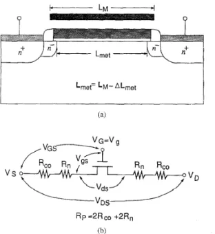
which represents the ‘effective’ channel region that can be strongly modulated by the gate bias, while the metallurgical channel length (L,e,t) is defined to be the distance between the metallurgical junctions of source and drain diffusions in the channel surface of a MOSFET, as illustrated in Fig. I(a).The extraction algorithms for effective channel length pro- posed in literatures were usually based on the resistance
[ 11-[8] and capacitance [SI, [IO] measurements. In addition to the problems of parasitic capacitance, equipment with high resolution is required to measure the small intrinsic gate capacitance down to the order of femto farads. Therefore, the capacitance method is impractical for applications. Comparing with the capacitance methods, the extraction algorithms based on the resistance methods are much simpler. Based on the Manuscript received August 11, 1995; revised December 7, 1996. The review of this paper was arranged by Editor K. Tada. This work was supported by the National Science Council, Taiwan, ROC, under Contracts NSC85-2215- E-009-041 and NSC84-2215-E009-019.
The authors are with the Advanced Semiconductor Device Research Labo- ratory and Institute of Electronics, National Chiao-Tung University, Hsinchu 30050, Taiwan, ROC.
Publisher Item Identifier S 001 8-9383(96)04041-5.
v s
Fig. 1. (a) The cross ection view of a LDD nMOSFET showing the definitions and the relationship among L,w, Lmet and AL,,t, and (b) the equivalent circuit of a practical MOSFET device.
resistance measurements, the methods [
11,
[2],[4]
determinedL,R
in a high gate overdrive range, which are applicable for conventional MOSFETs; while the method presented in [8] used a low gate overdrive range for LDD MOSFET’s. There is no definite method to determine the magnitude of gate overdrive.In this paper, an analytic equation is derived to predict the correct gate overdrive in order to determine the unique Lmet from the extracted L,R for both conventional and LDD MOSFET’s. In Section 11, a new extraction algorithm for the metallurgical channel length of MOSFET’s is described. Our new extraction algorithm is based on the resistance measurement, from which we can determine the effective channel-length reduction (AL,E). According to our analysis, the metallurgical channel-length reduction (AL,,,) can be determined from a wide range of gate-bias dependent A L e ~ .
To improve the accuracy, the threshold-voltage correction is performed iteratively. In Section 111, the 2-D numerical analy- sis shows that the major deviation in extraction arises from the nonideal resistance distribution due to carrier redistri- bution. In addition, an analytic model is proposed to evaluate this phenomenon, and comparisons between 2-D numerical 0018-9383/96$05.00 0 1996 IEEE
JEAN AND WU: NEW EXTRACTION ALGORITHM 941
analysis and analytic model evaluation are performed. The proposed extraction algorithm is verified by comparing the ex- traction results from 2-D simulation and experimental devices in Section IV. Finally, conclusions are given in Section V.
11. DESCRIPTIONS OF THE EXTRACTION ALGORITHM For an ideal MOSFET device operated in the linear (low drain bias) region, the drain current can be expressed as
where p is the effective channel mobility, which is a function of applied gate bias; Cox is the gate oxide capacitance per unit area;
we^
and L,ff are the effective channel width and length, respectively; V,, and V d , are the intrinsic gate to source and drain to source voltage drops, as shown in Fig. I@); andV, is the threshold voltage. If the total parasitic source/drain resistance is Rp and the source and drain are symmetrical, then we have
V
,
,
= VGS - I D s R P / ~ and Vds = VDS -I D S R P ,
where
IDS
is equal tola,.
Substituting V,, and V d s into (l), then the total resistance RT is given bywhere R,h is the channel resistance; L M is the mask channel length; and A L e ~ is the difference between mask channel length and effective channel length. If A L e ~ is assumed to be the same for all test devices in a testkey and the threshold voltage of all test devices are known exactly, we can determine
A L r ~
from (2) by the following steps:1) Taking the
RT
value versusL M
at the same gate overdrive for all devices, the slope (Slope) and the intercept in y-axis(Ycept)
can be obtained by a least squares fitting as followK e p t = RP - Slope x A L E . (4)
2) Varying the gate overdrive, we can get the variations of 3) Differentiating
K.ept
in (4) by Slope, we haveYccpt
with respect to Slope.Note that each A L e ~ at a given gate overdrive is deduced by its small gate overdrive interval, which is
a
constant within this small gate overdrive interval. Moreover, the extraction procedure described above needs to accurately determine the threshold voltages for all devices with different channel lengths Similarly, the effective channel mobility and the parasitic source/drain resistance are assumed to be constant within a small gate overdrive interval for all mask channel lengths. Theextracted overall effective channel-length reduction ( ALrff) in ( 5 ) is gate-bias dependent [l], [ 2 ] , [ 5 ] , [ 6 ] , and the detenni- nation of the metallurgical channel-length reduction from the gate-bias dependent effective channel-length reduction will be the major emphasis of this paper.
There are two basic guides to determine
ALrnet
from the gate-bias dependent A L e ~ :(a)
For conventional MOSFET devices, AL,E is chosen at higher gate overdrive [I]; (b) For LDD (lightly doped source/drain) MOSFET devices, AL,ff is chosen at lower gate overdrive [8]. The major reasons for using these two guides will be described in details in the next section. Once ALmet has been determined, the parasitic sourceldrain resistance ( R p ) can be derived.Rp
can be determined from (2) and is the value of RT whenLM
is equal to ALmet. Therefore, the definition of Rp is the total resistance outside the metallurgical junctions of source and drain diffusions. As mentioned above, for each gate overdrive there is a differentRp
because RP is gate-bias dependent. Nevertheless, the key step in channel-length extraction is to accurately determine the threshold voltage of each device so thatRT
can be evaluated at the same gate overdrive [7], [8]. With the improperly deduced threshold voltage, the extracted ALee will be far away from its exact value. Consequently, the threshold voltage must be determined accurately and carefully.In our extraction method, the normalized current method is used to determine the threshold voltage. First, the longest channel-length device is chosen to ensure negligible short- channel and parasitic source/drain resistance effects; and its threshold voltage is determined by the conventional maximum transconductance extrapolation method. The current at the extracted threshold voltage divided by the channel length is defined as the ‘normalized current’. Next, this ‘normalized current’ multiplied by other shorter channel length is used to determine the threshold voltage of shorter device. However, the channel length of shorter device before determining its threshold voltage is unknown except that the mask channel length is known. Therefore, initially the mask length is used instead of the channel length. This is a good approximation in the case of L M
>>
ALmet and will produce serious errors for small L M . In addition, it is known that the parasitic source/drain resistance Rp may greatly reduce the drain current of short channel devices. To reduce the influence of ALmet andRP
on the threshold-voltage determination, the ‘iteration’ method proposed in [8] is used. After extracting ALmet and Rp, from (2) we havewhere Ihs is the intrinsic drain current, which does not include the Rp effect. Therefore, we can determine VT from the extracted ALm,,t and ( 6 ) , and further to extract ALmet. This process is repeated until the extracted
V,
andALmet
self- consistently converge to their true values, as expressed by a flowchart shown in Fig. 2.111. NUMERICAL ANALYSIS AND
ANALYTIC MODEL EVALUATION
A. Numerical Analysis
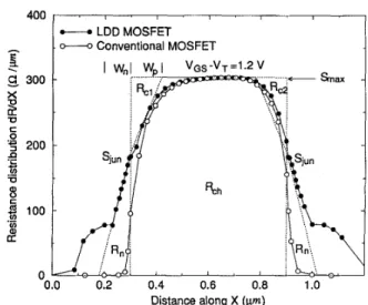
In the previous section, we have assumed that the MONS devices exhibit the ideal characteristics. The ideal resistance distribution is shown in Fig. 3 by the dashed line, in which
948 IEEE TRANSACTIONS ON ELECTRON DEVICES, VOL. 43, NO. 6, JUNE 1996
Determine V T from the Intrinsic Current with
Extracted Lmet
0.0 0.2 0.4 0.6 0.8 1.0 1.2 1.4
Distance along X ( p m )
and source-drain current [5]. Note that the area under the curve shown in Fig. 3 represents the resistance of a MOSFET. For an ideal device, the parasitic source/drain resistance (the resistance outside the Lmet region) is a fixed value and is independent of gate overdrive, whereas the channel resistance (the resistance in the Lmet region) is proportional to the metallusgical channel length Lmet and is bias-dependent. The maximum dR / d x (signed
S,,,)
must be the same for all channel lengths at a given gate overdrive. This means that the deduced threshold voltage is accurate, i.e., all devices are operated at the same gate overdrive. From the ideal devices shown in Fig. 3, the total resistance can be expressed aswhere R p = 2R,,
+
2R,; R,, is the contact resistance, which is not shown in Fig. 3; R, is the resistance between sourceldrain contact and channel region, as shown in Fig. 3. In general, R,, is constant, while R, is bias-dependent. Nevertheless,R,,
andR,
are all constants for the ideal characteristics. Now, Slope andYcept
in ( 5 ) can be obtained from (7): Slope = S m a x andYcept
= RP - S m a x xALmet.
According to ( 5 ) , the channel-length reduction can be obtained byd
AL., = --(Rp - Smax x AL,,t) (8)
dsmax
where Rcl and
Rc2
are the areas indicated in Fig. 3 and are bias-dependent, which represent the difference of channel resistance between ideal and practical MOSFET’s. On the other hand, the R, in the parasitic resistanceR p
is also dependent on gate overdrive for a practical device. Now, the total resistance of a practical MOSFET in (7) can be rewritten asRT
= 2Rc0+
A+
S
,
,
,
x (Ln/r - AL.,,t) (10) where A =2R,
-Rcl
- Rc2. From (lo),Ycept
becomesK e p t = 2 R c o
+
A - S m a x x ALmet. (1 1) Applying(3,
the extracted channel-length reduction becomes(12) d A
AL, =
AL,&
--.
dSmax
In practice, (1 2) is the effective channel-length reduction
AL,R as mentioned in the previous section. This equation described the relation between the extracted AL,R and the real
AL,,,.
If dA/dS,,, in (12) is equal to zero, the extracted AL,E will be equal to It is worth noting thatALmet
in (11) and (12) is a constant, while AL, and dA/dSmax are bias-dependent. The resistancesR,,
Rcl andRcz are all bias-dependent. Anyway, R,,
Rcl
and Rc2 cannot be extracted from the extraction algorithm as described in Section 11. Therefore, we compute these resistances fromJEAN AND WU: NEW EXTRACTION ALGORITHM
-
dle(ALeff)-
dAldSmax 0.4 0.3s.
0.2 v S.g
0.1 -1 0.0 -0.1 -0.2 0 1 2 3 4 5 6 7 Gate overdrive VGS -VT (V) Conventional nMOSFET t--.&e(ALeff)-
PdRnIdSmax-
-d(Rcl +RcZ)/dSmax 0.3t
2p
0.1 -1 0.0 -0.1 0 1 2 3 4 5 6 7 Gate overdrive VGS-VT (V) Fig. 4.device, and (b) conveutional device.
The simulation results using 2-D numerical analysis for (a) LDD
a 2-D device simulator-SUMMOS [ l l ] , as demonstrated in Fig. 4(a). In this figure, AL,R, dA/dS,,,, 2dR,/dSmax
and -(dRcl
+
dR,z)/dS,,, are computed as a function ofV i s - V, and the given
ALmet
is 0.2 pm. Note that AL,ff in Fig. 4 is calculated by(S),
where Slope(Smax) is obtained from Fig. 3,Ycept
is calculated byRT -
S m a x L ~ . As mentioned above, A L e ~ is bias-dependent and its value decreases from 0.5 pm to 0.1 pm when VGS - VT increases from 0 to 5V. Similarly, dA/dS,,, increases from negative to 0.1 pm. If we add
AL,ff
and dA/dS,,, together, the sum is nearly a constant, i.e., 0.2 pm, just the given value forALmet.
In other words, when dA/dS,,, is equal to zero, @.Lee is exactly equal to ALmet, and this situation happens at a gate bias ofVGS - VT = 1.8 V, as shown in Fig. 4(a). This means that the decrease rate of R,1
+
Rc2 is just compensated by the decrease rate of 2R,.Note that Figs. 3 and 4(a) are for LDD MOSFET's. For a conventional device, as shown in Fig. 5 , it is clearly shown that R, is nearly equal to zero because of the heavily doped sourceldrain region, so its gate modulation 2dR,/dS,,, in
949
400
-
, ' , ' , ' I / ! 'LDD MOSFET
-
Conventional MOSFET~
Fig. 4(b) approaches to zero. On the other hand, Rcl and Rc2 7 is constant.
0.0 0.2 0.4 0.6 0.8 1.0
Distance along X (pn)
Fig. 5. Comparisons of the resistance distribution between a LDD and a conventional MOSFET with Lmct = 0.6 p m for gate overdrive of 1.2 V. The resistances for a practical MOSFET device approximated by the simple geometrical shapes are also illustrated.
are similar for conventional and LDD MOSFET's. Hence, the curve of -(dR,1
+
dR,a)/dS,,, in Fig. 4(b) is similar to that in Fig. 4(a). Again, the sum of dA/dS,,, and ALeg is a constant. Apparent differences shown in this figure are AL,E and dA/dS,,,; unlike the LDD MOSFET's, AL,E anddA/dS,,,
approach to 0.2 and 0 pm at higher gate overdrive, respectively.From the 2-D numerical analysis for LDD and conventional MOSFET's mentioned above, the principle to choose ALmet from AL,g as described in the previous section has been given.
B. Analytic Model Evaluation
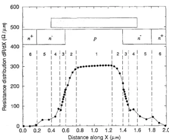
The resistance distribution of a typical MOSFET can be 1) Gate-controlled channel resistance,
2) Carrier diffusion related channel resistance, 3) Carrier diffusion related sourceldrain resistance, 4) Gate overlapped sourceldrain resistance, 5 ) Gate fringe field induced resistance, 6) Sourceldrain sheet resistance,
7) Contact resistance (not shown in Fig. 6).
divided into 7 components, as shown in Fig. 6. They are:
The gate-controlled channel resistance locates at the center of the channel and is strongly modulated by the gate volt- age. Components 2 and 3 come from carrier redistribution between sourceldrain region and channel region. Higher carrier concentration in sourceldrain region will diffuse to channel region where the carrier concentration is lower. This carrier redistribution decreases the channel resistance and increases the sourceldrain region resistance. Therefore, Component 2
is smaller than Component 1, while Component 3 is larger
than Component 4, as shown in Fig. 6. Components 4 and 5 are also modulated by gate bias, which are weak and very weak functions of gate bias, respectively. Component 6 is related to sourceldrain doping concentration and Component
950 IEEE TRANSACTIONS ON ELECTF-ON DEVICES, VOL. 43, NO. 6, JUNE 1996
0.0 0.2 0.4 0.6 0.8 1.0 1.2 1.4 1.6 1 8 2.0
Distance along X (pm)
Illustration of the practical MOSFET dewce divided into 7 regions Fig 6
according to the resistance distribution
Note that dA/dS,,, is an indicator of how AL,R approach- ing to QLmet. As the value
dAldS,,,
approaches to zero,QL,s
approaches to ALmet. Here,S,,,,
is a strong function of gate bias (Component l), and A is related to Components 2, 3 , 4 , 5 and 6. However, Component 6 is independent of gate bias and Component 5 is a very weak function of gate bias, so we can neglect them. Component 4 is basically a weak function of gate bias. For modern MOSFET devices, ALmet is small and, therefore, the overlapped region is further smaller than it. Again, Component 4 is abandoned. Now, we only consider Components 1, 2 and 3 to computedAldS,,,.
For a small drain to source voltage (e.g.,
VDS
= 0.05 V), the shape of Fig. 5 is nearly symmetrical, i.e., R,1=
Rc2. Therefore, dAldS,,, becomes(13) where
R,,
and R,1 can be approximated by the triangle areas shown in Fig. 5 and are given byRcl =
W,(S,,, - Sj,,)/2and
R,
= W,Sj,,/2, in which W, and W, are the widths of carrier redistribution in the channel and sourceldrain regions, respectively; Sj,, is the value ofd R l d x
at the metallurgical junction. Now, (13) becomesd
( 2 L - 2Rc1). -
-
dSmax
The exact values for W, and W, can be obtained by solving the current density and Poisson's equations. To simplify the problem, we consider that W, and
W ,
are proportional to Debye length in this paper. Since the majority-carrier con- centration deviated from the dopant concentration is governed by the extrinsic Debye length L D [12], which is expressed byL D =
[
-1
3 .
Therefore, W, and W , can be expressed as (15) Wn = ~ I L D , N k z [ q N D+
C~X(VGS - V F B ~ ) / Y ] - ~ (16)v (,+PI
wp
= ~ L D , p b [ c o , ( V ~ ~ - V T ) / Y ] - ~ ,where
kl
and IC2 are the constants;L D ,
and L D , are theextrinsic Debye length in the channel and source/drain region, respectively; CO, is the oxide capacitance per unit area; Y is the effective thickness of inversion and accumulation carriers; X, is the dopant concentration in the source/drain region;
V&, is the flat-band voltage in the source/drain region. The S,,, can be approximated by (referred to (3))
S m a x k:$(VGS - VT1-l (17)
where k3 is a constant, and we can evaluate
S,,,
from (17)simply by considering the channel resistance reduced by the built-in potential of the soul-ce/drain junction
S,,,
=
ks(Vc:s - VT+
VbJ1 (1 8) where Vblp is the built-in potential in the channel side. Substituting (15)-(18) into (14) and letting dA/dS,,, = 0, after some manipulations we haveSubstituting Y [13], VT,
VFB,
and vbip into (19), we cansolve
V&
by the iteration method. The results of the relation- ship among VGS -VT,
N o and N A (dopant concentration inthe channel region) are shown in Fig. 7. The adequate gate overdrive to determine for a fixed surface channel doping increases with the sourceldrain doping, because a larger gate overdrive is needed to accumulate the carrier density comparable to source/drain dopant concentration for heavily doped sourceldrain region, as shown in Fig. 4, where the higher sourceldrain doping results in weaker modulation for gate overdrive
on
the sourceldrain region. On the other hand, the gate modulation in the channel region becomes difficult as the gate overdrive increases due to strong inversion. So, a larger gate overdrive for heavily doped sourceldrain is needed to have dA/dS,,, approaching to zero for extracting ALmet. This also can be observed from (13), in which R,1+
Rc2 can be approximated by Wp(Smax - Sjun), as shown in Fig. 5, where W, in (15) a:ndS,,,
in (17) are independent of sourceldrain doping. Although Sj,, in (18) depends on sourceldrain doping through Vb;,-built-in potential in the channel side, it is a weak function of source/drain doping because source/drain doping is much higher than channel doping. Therefore, the gate modulation for R,1+R,z
is nearly the same for varied source/drain doping. However, 2R, NW,Sj,, strongly depends or1 sourceldrain doping through W ,
in (16), and this indicates that the gate modulation becomes weak when sourceldrain doping increases. In this situation, a weak gate modulation for R,l
+
R,z is needed to compensate it to let dAldS,,, = 0, which requires a higher gate overdrive.JEAN AND WU: NEW EXTRACTION ALGORITHM 95 1
-
E
=i
-
=-
Conv. MOSFET Without VT Correctioni)--oLDD MOSFET Without VT Correction
.
-
Conv. MOSFET With VT CorrectionParameter v a l u e Parameter
-
-
LDD MOSFET With VTCorrection
;;"
0.31
__ ALmetv a l u e
0 1 2 3 4 5 6 7
Gate overdrive VGS -VT (V)
Fig. 7. The adequate gate overdrive for extracting the Lmet versus Fig. 8. The relations of the extracted AL,R versus the gate overdrive for source/drain doping calculated by analytic evaluation and 2-D numerical conventional and LDD MOSFET's. The extraction results before and after simulation for various channel dopings. VT correction are shown.
On the other hand, the lower source/drain doping requires a lower gate overdrive to determine Lmrt.
For the channel concentration varies as large as two orders in magnitude, however, the adequate gate overdrive to determine
ALmet
does not show a large variation. This is convenient for our extraction algorithm, and we can determine ALmet without taking care of the channel doping. Moreover, then- region doping for LDD devices is around 10"
cmP3,
and the adequate gate overdrive is about 1.5 V. For conventional devices, the gate overdrive must be large enough to about5 V. Therefore, the principles for determining ALmet from AL,R are verified again. Simulation results from Fig. 4 and other cases are also marked in Fig. 7, the results agree well with those using the analytic model evaluation. Therefore, the deduced range of gate overdrive is a useful reference for our extraction algorithm.
In general, the parasitic source/drain resistance extracted from the algorithm described in the previous section will be smaller than the exact value (if ALmet is correct). This can be observed from (lo), if we let L M = ALnlet,
RT
will be equal to 2R,, +2R, -RC1
-Rc2
and this value is smaller thanRp = 2R,,
+
2R, byR,1
+
Rc2. So, we can predict that the extracted Rp will deviate from its exact value, especially when the the gate overdrive is small and the deviation is extremely large (Fig. 9). However, the extracted RP is very accurate at high gate overdrive.I v . EXTRACTION RESULTS
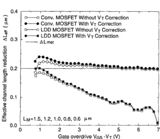
The parameters given in our simulation are listed in Table I for conventional and LDD MOSFET's, and the definitions for the parameters are given in [ l l ] . The mask channel lengths used are L M = 1.5, 1.2, 1.0, 0.8, 0.6 pm. The extraction results for conventional and LDD MOSFET' s with and without V, correction are all shown in Fig. 8. The AL,t-f for conventional devices approaches to
ALmet
at aroundV& -
VT
= 5 V, this agrees with the conclusions in the previous analysis (Fig. 7). TheV
,
correction is not impor-tant because Rp of conventional device is small. For LDD devices without VT correction,
A L e ~
is always smaller than ALmet. After VT correction,A L e ~
is equal to ALmet at a gate overdrive of about 1 V. The gate overdrive does not precisely agree with the analysis (Fig. 7) due to the assumptions of constant Rp and p, and the error is introduced in the extraction process. For convenience without losing the precision of ALmrt extraction, the maximum ofAL,R
is chosen to be ALnlet for LDD devices. On the contrary, we regard AL,s at high gate overdrive (e.g., 5 V) as ALmet for conventional devices. However, it is not adequate to choose a very high gate overdrive because S,,, (averaged channel resistance) decreases very slowly at high gate overdrive, thereforedAldS,,,
is prone to induce enormous error by noise. On the other hand, as shown in Fig. 4(b), -d(R,1t-
Rc2) /dS,,, approaches to zero at high gate overdrive, but 2 d R ,
Ids,,,
increases slowly. If a very high gate Overdrive is chosen, ALrrlet will be underestimated. This means that at the very high gate overdrive a part of source/drain region becomes channel region, therefore reducing ALeff. In practice, we take the average of A L e ~ in the range of 4 N 5 V in order952
L13343-19
IEEE TRANSACTIONS ON ELECTRON DEVICES, VOL. 43, NO. 6, JUNE 1996
140 . 0.181 0.188 0.185
z
x 1017L ~ = 1 . 5 , 1.2, 1.0, 0.8, 0.6 pm
o---o Computed Rp of C o w . MOSFET D--O Computed RP of LDD MOSFET
-
-
Extracted Rp of Conv. MOSFET Extracted Rp of LDD MOSFET G t L23003-36 a I4O . 0.334 0.404 0.395 l O I 7 0 " " " " " " " ' 0 1 2 3 4 5 6 7 Gate overdrive V,, -V, (V)Comparisons between the computed and extracted parasitic resistance Fig. 9.
versus gate overdrive for conventional and LDD MOSFET's.
TABLE I1
THE EXTRACTION RESULTS FROM CONVENTIONAL AND LDD
STRUCTURES. THE PARAMETERS LISTED ARE DIFFERENT FROM TABLE I DEVJCES BEFORE AND AFTER
v~
CORRECTION FOR VARIOUSI I I I I T,,=lOO d 0.197/0.162 0.202/0.191 f = 0.9 0.197/0.188 0.201/0.201 E,, = 250 0.202/0.186 0.206/0.199
L
AL.,,, = 0.5pm 0.506/0.452 0.509/0.503The extracted and computed (from simulator)
Rp
are plotted in Fig. 9. As indicated, the largerRp
values emphasize the im- portance of VT correction for LDD devices. For conventional devices,Rp
at low gate overdrive is smaller than that at high gate overdrive. This is due to large RC1, Rc2 and smallR,
at low gate overdrive. However, for LDD devices, the behaviors ofRC1
and Rc2 are similar to those of conventional devices, butR,
is large enough to compensate R,1 andRcz.
SoR p
still increases: unlike the conventional devices, it decreases as the gate bias is reduced. Anyway, the extracted R p is always smaller than the computed results using a simulator at any gate overdrive for both devices, because we cannot evaluate
RC1
andR,z.
To verify the validity of this extraction algorithm for various device structures, many cases are simulated by the SUMMOS. In addition to the previous case, other cases for different channel dopings, oxide thicknesses, lateral diffusion coef- ficients, contact resistances and AL,,, are examined. The parameters used and the extraction results are listed in Table I1 for conventional and LDD devices. It is shown that fairly good agreements are obtained. Again, we find that the V,
TABLE 111
COMPARISONS OF THE EXTRACTION RESULTS BETWEEN THIS ALGORITHM AND THE METHOD PROPOSED IN [ 151
L13343-15 140 0.180 0.195 0.215
6 x 10¹⁶
I
L13343-32
E-1
0.1661
0.1701
0.210I
correction is more important for LDD than conventional devices. Comparing the extracted A Lmet with the given value, the variations for all cases are smaller than 0.01 pm. This indicates that our extraction algorithm is valid for all device structures.
The conventional devices consisting of different oxide thick- nesses and channel concentrations are fabricated, and the I-V characteristics are measured by HP-4145B. Applying our extraction algorithm to the I-V characteristics of these devices, the extraction results are listed in Table 111. In Table 111, wafer Nos. 5, 17 and 32 have different oxide thicknesses with the same channel doping, the extraction results show that
AL,,,
is 0.170 pm with small variation. A quite reasonable conclusion can be drawn for these cases-the oxide thickness doesn't influenceAL,,,.
However, wafer Nos. 15, 17 and 19 have different channel implantation doses with the same oxide thickness, the extractedALmet
value varies from 0.170 to 0.195 pm. In theory, the higher channel concentration should reduceAL,,,
slightly. This phenomenon is not shown in Table 111. The discrepancy may be resulted from the nonuniform channel profile in the lateral direction due to the reverse short channel effect, which is more serious for heavy channel implantation [ 141.The test devices with the LDD structure are also fabricated and examined, as shown in Table 111, in which a novel channel- length extraction method using the charge pumping technique
[ 151 is also performed. Comparing with our extraction results, it is shown that very good agreements are obtained.
V. CONCLUSION
A new extraction algorithm for the metallurgical channel length and the parasitic resistance of conventional and LDD MOSFET's is described. With our proposed technique, the errors induced by channel-length uncertainty and the effects of parasitic source/drain resistance on the threshold voltage are reduced. A 2-D numerical analysis is performed to analyze the factors affecting the effective channel length, and the ex-
JEAN AND WU: NEW EXTRACTION ALGORITHM 953
traction principles for A
Lmet
are proposed. The principles for extracting the metallurgical channel length deduced from the 2-D numerical analysis are also evaluated by a simple analytic model. Comparing with 2-D numerical analysis, the analytic model evaluationis
proven to bea
reasonable approximation. The proposed extraction algorithm has been verified by the simulated I-V characteristics, and the error is within 0.01 pm. Moreover, the parasitic source/drain resistance is also extracted, and it is shown that smaller parasitic resistance at low gate overdrive is inevitable. Compared with the computa- tion results, the extraction results are fairly accurate. Applying this extraction algorithm to the experimental devices and comparing with the results extracted by the charge pumping method, it is shown that very good agreements between these two methods are obtained.ACKNOWLEDGMENT
The authors would like to express their sincere thanks to the National Science Council, Taiwan, Republic of China, for continuous grant support. Special thanks are given to the Elec- tronics Research and Service Organization (ERSO), Industrial Technology Research Institute (ITRI), Taiwan, Republic of China, for providing the test devices.
REFERENCES
111 K. Terada and H. Muta, “A new method to determine effective MOSFET channel length,” Jpn. J. Appl. Phys., vol. 18, no. 5 , p. 953, May 1979. [21 J. G. J. Chern et al., “A new method to determine MOSFET channel length,” IEEE Electron Device Lett., vol. EDL-1, no. 9, p. 170, Sept. 1980.
[3] F. E. de la Moneda et al., “MCdSUR“ent of MOSFET constants,” IEEE Electron Device Lett., vol. EDL-3, no. 1, p. 10, Jan. 1982.
[4] K. L. Peng et al., “Basic parameter measurement and channel length broadening effect in submicronmeter MOSFET,” IEEE Electron Device Lett., vol. EDL-5, p. 473, Nov. 1984.
151 S. E. Laux, “Accuracy of an effective channel length/external resistance extraction algorithm for MOSFET’s,” IEEE Trans. Electron Devices, vol. ED-31, no. 9, p. 1245, Sept. 1984.
161 C. J. Hu e f al., “Gate-voltage-dependent effective channel length and serious resistance of LDD MOSFET’s,” IEEE Trans. Electron Devices, vol. ED-34, no. 12, p. 2469, Dec. 1987.
171 Y. Taur et al., “A new ‘shift and ratio’ method for MOSFET channel- length extraction,” IEEE Electron Device Lett., vol. EDL-13, no. 5, p. 267, May 1992.
[XI J. Y.-C. Sun et al.. “On the accuracy of channel length characterization of LDD MOSFET’s,” IEEE Trans. Electron Devices, vol. ED-33, no. 10. p. 1556, Oct. 1986.
[9] B. .I. Sheu and P. K. KO, “A capacitance method to determine channel length for conventional and LDD MOSFET’s,” IEEE Electron Device Lett., vol. EDL-5, no. 11, p. 10, Nov. 1982.
[ I O ] S.-W. Lee, “A capacitance-based method for experimental determination of metallurgical channel length of submicron LDD MOSFET’s,” IEEE Trans. Electron Devices, vol. ED-41, no. 3, p. 403, Mar. 1994. [I11 R. K. Perng, “An efficient two-dimensional MOS simulator (SUMMOS)
and it5 application,” Ph.D. Dissertation, Inst. of Electronics, National Chiao-Tung University, Taiwan, R.O.C, July 1991.
1121 W. C. Johnson and P. T. Panousis, “The influence of Debye length on the C-V measurement of doping profiles,” IEEE Trans. Electron Devices, vol. ED-18, no. 10, p. 965, Oct. 1971.
[I31 S. A. Schwarz and S. E. Russek, “Semi-empirical equations for electron velocity in silicon: Part 11-MOS inversion layer,” IEEE Trans. Electron Devices, vol. ED-30, no. 12, p. 1634, Dec. 1983.
[14] M. Orlowski et al., “Submicron short channel effects due to gate reoxidation induced lateral interstitial diffusion,” IEDM Tech. Dig., p.
632, 1987.
[15] H. H. Li and C. Y. Wu, “A novel extraction technique for the effective channel length of MOSFET devices,” IEEE Trans. Electron Devices, vol. 42, no. 5 , p. 856, May 1995.
Yuh-Sheng Jean (S’90) was born in Taiwan, Republic of China, on July 5, 1968. He received the B.S. degree in electrical engineering from the National Central University, Taiwan, in 1990. He is currently working toward the Ph.D. degree in
the Institute of Electronics, National Chiao-Tung University. His research areas focus on deep- submicrometer MOS device physics and reliability issues.
Ching-Yuan Wu (M’72) wa\ born in Taiwan, Republic of China, on March 18, 1946 He received the B S. degree in electrical engineering from the National Taiwan University, Tdiwan, in 1968, and the M S and P h D degrees from the State University of New York at Stony Brook in 1970 and 1972, respectively
During the 1972-1973 academic year, he was appointed a\ a Lecturer, Department of Electronical Sciences, SUNY-Stony Brook. During the 1973-1975 academic years, he was a Visitin;; Associate Professor at the National Chiao-Tung University (NCTU), Taiwan In 1976, he became Full Professor in the Department of Electronics dnd the Institute of Electronics at NCTU While there he wd\ the Director of the Engineering Laboratories and Semiconductor Re\earch Center from 1974 to 1980, the Director of the Institute of Electronic\ from 1978 to 1984. and the Dean of the College of Engineering from 1984 to 1990 He was a
principal investigator of the National Electronics Mass Plan-Semiconductor Devices and Integrated-Circuit Technologies from 1976 to 1979, and had been a Coordinator of the National Microelectronic5 Re\earches and High- Level Man-Power Education Committee, National Science Council, Republic of China from 1982 to 1988. He ha5 been the Revearch Consultant of the Electronics Research and Service Organization (ERSO), ITRI, a member of the Academic Review Committee in the Ministry of education, and the chairman of the Technical Review Committee on Information and Microelectonic 5
Technologim at the Ministry of Economic Affairs His reyearch activities have been in semiconductor device physics and modeling, Integratecl- circuit designs, and technologies His current research area? focus on the developments of efficient 2D and 3D simulators for deep-submicrometer semiconductor device\, design rules and optimization techniques for d e e p submicrometer CMOS device\. He has published over 180 papers in the semiconductor field and has served a5 a reviewer for international journals such as IEEE ELECTRON DEVICE LETTERS, IEEE TRANSACTIONS ON ELECTRON DEVICES and Solid State Electronics.
Dr. Wu is a member of the Honorary Editorial Advisory Board of Sold State Electronics, and is a board member of the Chinese Engineering Society He received the Academic Research Award in Engineermg from the Ministry of Education (MOE), in 1979 and the Outstanding Scholar Award from the Chinese Educational and Cultural Foundation in 1985. He received the outstanding research Professor fellowship from the Ministry of Education arid the National Science Council (NSC), Republic of China from 1982 to 1995 He received the Distinguished Engineering Professor Medal Award from the Chineae Engineering Society in 1992