The Circle-grid Electrode on Concentrated GaAs Solar Cells Efficiency
Chen-Chen Chung, Hung-Wei Yu, Li-Han Hsu, Chien-I Kuo, Nguyen-Hong Quan, Yu-Sheng Chiu and Edward Yi Chang
Department of Materials Science and Engineering, National Chiao Tung University, R409, MIRC. 1001 University Rd., Hsinchu, Taiwan 30010, R.O.C.
The relationship between front contact pattern of GaAs single-junction solar cell with conversion efficiency at different concentration ratios is studied in this paper. Five different front circle-grid patterns were designed and patterned on the in-house fabricated single junction GaAs solar cells. At high light concentration ratio, the cell efficiency is strongly dependent on the series resistance of the electrode. At the same time, the thermal effect should also be taken into consideration, especially when a device is operating under high concentration ratio. Therefore, the aim of this work is to find a suitable front contact pattern for a GaAs single-junction solar cell to increase the conversion efficiency under high concentration solar radiation. It is found that the device with proper pattern design geometrical shadowing factor of 7.1% has the best cell efficiency of 27.05% at CR>100x, AM1.5G.
Introduction
Global-warming issues coupled with high oil prices have become a major driving force for the use of advanced solar power technology. III-V solar cell is so far the commercial solar cell with highest efficiency and they will play an important role in future high-efficiency and low-cost photovoltaic cells industry [1]. III-V compound semiconductors are promising materials for achieving high reliability and high performance in optoelectronic devices. However, III-V solar cell is a promising technology due to several advantages such as higher efficiencies of up to 25%, a nearly ideal band gap (1.42 eV) for single-junction solar cell, a higher absorptivity, relatively insensitive to temperature variation, and having better radiation resistance than silicon [2]. All these properties make GaAs become a very desirable material for space applications. There are several important parameters that effect the solar cell efficiencies including effective photon absorption, carrier separation, and carrier collection [3, 4]. Besides, the conversion efficiency of a solar cell depends on the antireflection (AR) coating, recombination loss, ohmic contact, and for III-V solar cell, electrode patterns is particularly important [5].
Among of these several parameters, the shadowing factor is the most important one that influences the amount of incident light and series resistance of front contact especially when a solar cell is operated under a high concentration ratio, the high-intensity incident light will generate large photocurrent and consequently induce a loss path due to the Joule effect. Besides, there is an antagonism problem between the shadowing effect and the series resistance [6].
For the concentrated solar cell, the design of the contact pattern is quite different from conventional silicon solar cell. In fact, various shadowing factor for the incident light and series resistance of the solar cell were influenced by the geometry of the front contact
pattern. In this respect, in order to get the best conversion efficiency, the choose of an optimal front contact for solar cell becomes more and more important, especially when a solar cell is operated under a high concentration ratio of light [7]. Therefore, in this paper, we tried to figure out how these two effects influence the solar cell efficiency and how to attain maximum conversion efficiency. Five different circle-grid electrode patterns of the front contact were designed and fabricated on the GaAs solar cells with the consideration of collecting more photocurrent, reducing the series resistance, lowering shadowing effect, and increasing the conversion efficiency.
Experiment
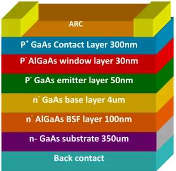
The schematic diagram of the GaAs single junction solar cell is shown in Fig. 1. The structure was grown in a commercial metal-organic chemical vapor deposition (MOCVD) reactor. The reactant gases were trimrthylindium (TMIn), trimethylgallium
(TMGA), trimethylaluminum (TMAl), arsine (AsH3), and phosphine (PH3). The doping
sources for n-type and p-type GaAs were silane (SiCH4). These sources were carried out
into the reactor by purified hydrogen that diffuses though a palladium cell.
The layers listed in Fig. 1. were obtained by optimizing growth conditions such as III/ V ratio, dopant type, exposure time to reactant gases and growth temperature (600-700
oC). The cascade structure consists of five layers, starting with a n-GaAs substrate,
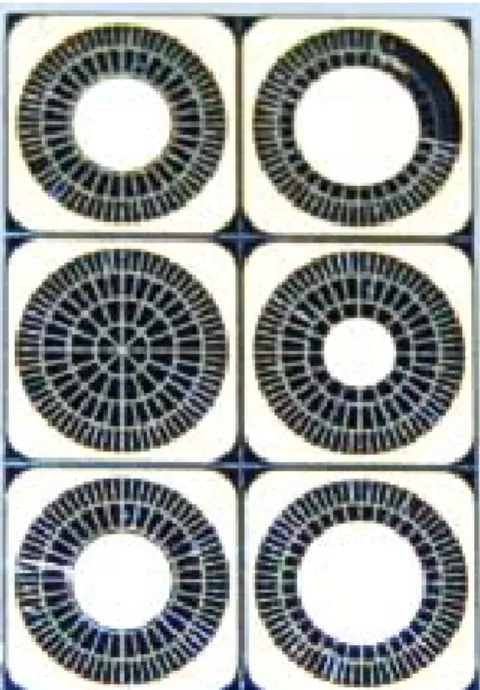
followed by n at p type, AlGaAs at GaAs layers. Finally, the cell structure is terminated with highly-doped GaAs cap layer of 300nm thickness for better ohmic contact. The front and back ohmic contacts were formed by Ti/Pt/Au and Ni/Ge/Au/Ni/Au, respectively. Here, five different circle-grid patterns were designed for the front contact of the GaAs single junction solar cells. Fig. 2 shows all the designed patterns, they are with the same grid length and spacing except for different percentages of shadowing factor for the center spot. The geometrical shadowing factors are shown in Table 1. In order to obtain better electrical properties, the top circle-grid patterns were subsequently plated with Au to a total thickness of about 5μm. Finally, a thickness of 750 Å silicon nitride AR coating
film was deposited by PECVD system. The area of the samples is 4.4×4.4 mm2 with
illuminated active area of about 0.125 cm2. Then the I-V characteristics were measured
under one sun AM1.5 (100mw/cm2) with an ISO-standard AM1.5 solar simulator. Figure
Back contact n- GaAs substrate 350um
n- AlGaAs BSF layer 100nm
n- GaAs base layer 4um
P- GaAs emitter layer 50nm
P- AlGaAs window layer 30nm
P+ GaAs Contact Layer 300nm
ARC
Fig. 1 The schematic structure of the single-junction GaAs solar cell.
R5 00 R1,0 00 R1,50 0 R2,000 4,400 4, 40 0 100 80 4,200 4, 20 0 R600 N=8 N=16 10 N=32 N=64 30 (A) (B) R2,000 R1,50 0 R1,000 N=16 10 N=32 N=64 R6 50 4, 200 4, 400 4,200 4,400 R600 (C) 4,400 4,200 4, 4004,200 R600 R2,00 0 R1,50 0 R1,0 00 N=16 10 N=32 N=64 R900 (D) N=32 N=64 10 R1,50 0 R2,000 R1,1 50 4,400 4,200 4, 4004,200 R600 (E) Fig. 2 Fabricated circular grid patterns for the front contact of solar cell.
Table 1 The shadowing factors for the front contact patterns.
Grid Pattern A B C D E
Shadowing
Fig. 3 Photograph of the fabricated GaAs single-junction solar cells.
Results and Discussion
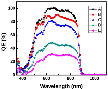
Fig. 4 shows the measured quantum efficiency (QE) of the GaAs single junction solar cell with five different grid patterns. The quantum efficiency of solar cell is defined by the following equation:
( )
λ hc qφ( )
λJ
QE = sc /
[1]
The quantum efficiency at a given wavelength λ is defined as where Jsc (λ) is the total
photo generated short-circuit current density at a given wavelength λ; (λ) is the
photon flux of the corresponding incident light and q is the elementary charge [8]
.
Itshows the ability of generating electron-hole pairs due to by the incident photon. The quantum efficiency of pattern A is 100%, pattern B is 90%, pattern C is 80%, pattern D is 50% and pattern E is 30%. It is clearly observed that the shadowing factor of the pattern A (shadowing factor = 6.2%) is the smallest of these five different devices but has the highest quantum efficiency due to more photon absorbed in the devices which increased the short current density. Fig. 5 shows the measured I-V curve of these devices with different circle-grid patterns under 1 sun (100mW/cm2, AM1.5G). As we can see, the device with pattern A has the highest efficiency of about 28.5% due to large amount of incident light caused by the smallest shadowing factor of the contact pattern [9]. However, when a solar cell operated under higher light concentration condition (CR>100x, AM1.5G), the thermal effect should be taken into account. For a concentrated solar cell, the effect of current crowding may occur at the center of the device due to the focused incident light [10, 11]. Fig. 6 shows the efficiency of the solar cell with different contact patterns investigated under different concentration ratios. At low and high concentrate ratios, the measurement results show that for lower concentration ratio (34x, AM1.5G), the device with front contact pattern A (shadowing factor = 6.2%) still has the best cell efficiency of 28.5%. However, at higher concentration ratio (CR>100x, AM1.5G), the device with front contact pattern B (shadowing factor = 7.1%) showed the highest
efficiency of about 27.05%. Although pattern B has larger shadowing factor than pattern A, the larger contact area in the center spot can improve the heat dissipation, resulting in lower series resistance and better cell efficiency.
400 600 800 1000 0 20 40 60 80 100
QE (%)
Wavelength (nm)
A B C D EFig. 4 Quantum Efficiencies of the single junction GaAs solar cells with different grid patterns. 0.0 -0.2 -0.4 -0.6 -0.8 -1.0 -1.2 -1.4 0.0 0.5 1.0 1.5 2.0 2.5 3.0 3.5
Isc (mA)
Voc (V)
A B C D EFig. 5 Current-voltage characteristics of the single junction GaAs solar cell with different grid patterns.
0 20 40 60 80 100 120 140 160 20 22 24 26 28 30 A B C D E
EFF. (%)
CR
Fig. 6 The Efficiency vs concentration ratio of single-junction GaAs solar cell with different circle-grid patterns.
Conclusion
In this paper, the relationship between front contact pattern and conversion efficiency of GaAs single-junction solar cell is investigated under different light concentration ratios and pattern designs. Regarding to the front contact pattern, there is an antagonism between the shadowing effect and series resistance effect. For a concentrated solar cell, the effect of current crowding may occur at the center of the device due to the focused incident light. The measurement results show that in the low concentration ratio (CR=35x, AM1.5G), the device with front grid pattern A (shadowing factor = 6.2%) has the best cell efficiency of about 28.5%. However, in higher concentration ratio (CR>75x, AM1.5G), the device with front grid pattern B (shadowing factor = 7.1%) shows the best cell efficiency of 27.05%, which is due to the improvement of heat dissipation at the center spot.
References
1. H. F. MacMillan, H. C. Hamaker, N. R. Kaminar, M. S. Kuryla, M. Ladle Ristow, D. D. Liu and G. F. Virshup, Proc. 20th IEEE PVSC, pp. 462-468 (1988).
2. F. Dimroth, “High-efficiency solar cells from III-V compound semiconductors” phys.stat.sol (2006).
3. J. Zhao, A.Wang, P. Altermatt, M. A. Green, Appl. Phys. Lett. 1995, 66, 3636.
4. J. Zhao, A. Wang, M. A. Green, F. Ferrazza, Appl. Phys. Lett. 1998, 73, 1991.
5. S.E. LEE, S.W. Choi, J. Yi, Thin Solid Films (2006).
6. A Cheknane, B.Benyoucef, J-P. Charles and R.Zerdoum, J.of Active and Passive Electronic Devices, Vol. 1, pp.1-11 (2005).
7. Z.H. Lu, Q. Song, S.Q. Li, Q. Yao, Proceedings of ISES Solar Word Congress (2007).
8. E.T.Franklin, and J.S Coventry, Proceedings of Solar 2002 - Australian and New Zealand Solar Energy Societ.
9. Martin A. Green “Solar Cells Operating Principles, Technology, and System Applications” P85~102.
10. V.M. Andreev, V.A. Grilikhes, V.D. Rumyantsev “Photovoltaic Conversion of Concentrated Sunlight” P73~87.
11. M.Y, T.T, K.A, N E-D, “ Multi-junction III-V solar cell: current status and future potential” Solar energy (2005).