Formation of CrZO and CrZNZO ®lms serving as Cu oxidation resistant
layers and their N
2
pre-sintering effect
Jui-Chang Chuang*, Mao-Chieh Chen
Department of Electronics Engineering and the Institute of Electronics, National Chiao-Tung University,1001 Ta Hsueh Road, Hsinchu, 300, Taiwan Received 19 March 1998; accepted 12 June 1998
Abstract
This study investigates the Cu oxidation resistant layers of sputter deposited CrZO and reactively sputter deposited CrZNZO of 200 AÊ thickness, with and without, thermal N2pre-sintering treatment. The resistance against Cu oxidation (or the highest annealing temperatures
without causing Cu oxidation) of the CrZO and CrZNZO covered Cu ®lms were found to be 350 and 5008C, respectively, in an O2ambient.
The inherent defects in the CrZO layers and the nitrogen doping in the CrZNZO layers were believed to be the principal causes for the distinction of the resistance against Cu oxidation. With N2pre-sintering treatments on the CrZO or CrZNZO covered Cu ®lms, the ability of
resistance against Cu oxidation was degraded. The higher the N2pre-sintering temperature was, the lower the oxidation temperature of Cu
became. The N2pre-sintering thermal process led to formation of defects on the CrZO and CrZNZO layers, resulting in the degradation of
the ability of resistance against Cu oxidation. Thus, the application of CrZO or CrZNZO as a resistant layer against Cu oxidation should avoid such an excess thermal treatment. q 1998 Elsevier Science S.A. All rights reserved.
Keywords: Chromium; Copper; Oxidation; X-ray photoelectron spectroscopy
1. Introduction
Copper (Cu) has been studied extensively as a potential substitute for aluminium (Al) and Al-alloys in multilevel-metallization of semiconductor devices and integrated circuits [1]. Compared with Al and Al-alloys, Cu has a number of bene®cial factors, such as lower bulk resistivity, higher electromigration resistance, higher melting point, and lower reactivity with commonly used diffusion barrier materials. However, Cu has its drawbacks with respect to the applications in Si-based integrated circuits, such as dif®-culty in dry etching, poor adhesion to dielectric layers (SiO2), fast diffusion in silicon and SiO2, deep level trap
in silicon, and formation of Cu silicides at low temperatures [1±3]. Meanwhile, another issue of interest concerns the easy oxidation of Cu exposed to the oxidizing ambient. It is well known that Cu oxidizes easily in air and in humid ambient [4], even at room temperature. This character has deferred the application of Cu in integrated circuits. Proper techniques must be developed to alleviate this problem before the application of Cu becomes feasible [5]. A number of studies have been reported that concern the oxidation-resistant Cu ®lms doped with or covered by oxidation
resis-tant metals [6±11]. Moreover, it has also been reported that the formation of metal silicide [12] on the surface of Cu ®lms and the boron implantation into Cu ®lms [13] provided superior oxidation resistance. In this study, thin ®lms of the sputter deposited CrZO and reactively sputter deposited CrZNZO layers are used as resistant layers to protect Cu ®lms from easy oxidation at high temperatures in an oxidiz-ing ambient. In addition, we also evaluate the effects of thermal N2pre-sintering on the oxidation resistance of the
CrZO and CrZNZO covered Cu ®lms. 2. Experimental details
The starting materials were p-type boron-doped 3-inch diameter Si wafers with a nominal resistivity of 17±55 V cm. After an initial RCA cleaning [14], the Si wafers were thermally oxidized at 10508C in steam atmosphere to grow 5000 AÊ of SiO2. A 2000 AÊ Cu ®lm was sputter deposited on
the SiO2layer. This was followed by sputter deposition of a
200 AÊ thick cover-layer using a pure Cr target in an Ar ambient or in an ambient of (N21Ar) gas mixture at a
pres-sure of 7.8 mTorr without breaking the vacuum. A DC magnetron sputtering system was used for the ®lm deposi-tion, and the base pressure of the system was about 1 £ 1026
Torr. Since Cr is an inherent oxygen absorber [15,16],
0040-6090/98/$ - see front matter q 1998 Elsevier Science S.A. All rights reserved. PII S0040-6090(98)00979-1
* Corresponding author. Tel.: 1 886 3 5712121, ext. 54156; fax: 1886 3 5724361; e-mail: mcchen@cc.nctu.edu.tw.
oxygen was automatically incorporated into the sputtered ®lms. The layers sputter deposited in pure Ar ambient are designated as `CrZO' layers, while those reactively sputter deposited in (N21Ar) gas mixture with an N2partial
pres-sure of 1.56 mTorr are designated as `CrZNZO' layers. The deposition rates of CrZO and CrZNZO layers were controlled to about 0.3 AÊ/s. The atomic concentration ratio of compositional elements in the CrZNZO layer was Cr : N : O 45 : 30 : 25, as determined by Auger elec-tron spectroscopy (AES). For the simplicity of reference, the Cu ®lms covered by CrZO and CrZNZO layers are desig-nated as sample A and sample B, respectively. After the deposition of CrZO or CrZNZO layers, wafers were diced into 1:5 £ 1:5 cm2pieces. The diced sample A's and
sample B's were thermally sintered in an N2ambient for 30
min at 300, 500, and 7008C, and were further designated by subscripts of `3N', `5N', and `7N', respectively. Meanwhile, samples without N2sintering treatment were further
desig-nated by a subscript of `AS' for identi®cation. To study the resistance against Cu oxidation, each sample, with or with-out N2sintering treatment, was thermally annealed in an O2
¯owing furnace for 50 min at temperatures ranging from 100 to 6008C. For identi®cation purpose, we designated, for example, sample A without N2pre-sintering treatment
but thermally annealed at 5008C in O2as `AAS500O', and
sample B with 5008C N2pre-sintering treatment and
ther-mally annealed at 3008C in O2as `B5N300O'.
The abrupt sheet resistance change of samples was used as a criterion for failure of resisting Cu oxidation. The samples before and after the failure were further character-ized by various techniques of material analysis. A 4-point probe was used to measure the sheet resistance. X-ray diffraction (XRD) analysis was used for phase identi®ca-tion. Scanning electron microscope (SEM) was used to investigate the surface morphology. Secondary ion mass spectroscopy (SIMS) was used for depth pro®le analysis. Moreover, X-ray photoelectron spectroscopy (XPS) was used to characterize the chemical states of compositional elements.
3. Results
3.1. CrZO/Cu/SiO2/Si
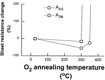
Fig. 1 shows the sheet resistance change for samples AAS
and A3Nafter thermal annealing in O2ambient at a couple of
temperatures. Abrupt change of sheet resistance was observed at temperatures higher than 3508C for sample AASand 3008C for sample A3N. For samples A5Nand A7N,
which were N2pre-sintered at higher temperatures of 500
and 7008C, respectively, the abrupt change of sheet resis-tance occurred at an O2annealing temperature below 3008C;
in addition, the oxidized ®lms peeled off the SiO2substrate.
Fig. 2 shows the XRD spectra for sample A's before and after annealing in O2 ambient at temperatures around the
abrupt change of sheet resistance. The spectra of sample AAS's, which were not N2 pre-sintered, revealed (2111)
and (200) orientations of CuO phase after O2annealing at
4008C (the AAS400O spectrum); for the AAS and the Fig. 1. Sheet resistance change vs. O2annealing temperature for samples
AASand A3N.
Fig. 2. XRD spectra for the O2annealed CrZO/Cu/SiO2/Si (sample A): (a)
samples without N2pre-sintering treatment, (b) samples with N2
pre-sinter-ing treatment at 3008C and (c) samples with N2pre-sintering treatment at
AAS350O samples, only Cu phase was observed; thus, the
resistance against Cu oxidation of the CrZO layer without N2 pre-sintering treatment was de®ned to be 3508C. In
contrast, copper oxide phases appeared on all the N2
pre-sintered samples (samples A3N, A5N, and A7N) after O2
annealing at temperatures above 3008C (Fig. 2b,c) with the diminishing peak intensity of Cu(111) phase. Fig. 3 shows the SIMS depth pro®les for samples AAS300O and
A5N300O. It is clear that the sample A5N300O had lost its
original layered structure. This further con®rms the degra-dation of the ability of resistance against Cu oxidegra-dation by N2
pre-sintering treatment. 3.2. CrZNZO/Cu/SiO2/Si
Fig. 4 shows the sheet resistance change for samples BAS,
B3N, and B5Nafter annealing in O2ambient at a number of
temperatures. Abrupt change of sheet resistance was observed at temperatures higher than 5008C for sample BASas well as B3Nand 4508C for sample B5N. By comparing
the result for sample AAS(Fig. 1) with that for sample BAS
(Fig. 4), we found that the ability of resistance against Cu oxidation of the CrZNZO layer was 1508C higher than that of the CrZO layer. However, similar to the case of CrZO layer, N2 pre-sintering treatment on the CrZNZO layer
degraded the ability of resistance against Cu oxidation too. Fig. 5 shows the XRD spectra for sample B's before and after annealing in O2ambient at temperatures around
the occurrence of abrupt sheet resistance change. The spec-tra for samples B3N's (not shown) were similar to those of
samples BAS's (Fig. 5a). The CuO phase appeared after
5508C annealing for sample BASwhile only Cu(111) phase
was observed for the samples annealed at as well as below 5008C. However, for the 5008C N2 pre-sintered samples
(samples B5N's), the CuO phase appeared after O2annealing
at 5008C (Fig. 5b). Fig. 6 shows the SIMS depth pro®les for samples BAS500O and B5N500O. The loss of layered
struc-ture for sample B5N500O (Fig. 6b) indicated the degradation
of the ability of resistance against Cu oxidation by N2
pre-sintering treatment.
Based on the illustration presented above, we concluded that the appearance of CuO phase coincided with the abrupt change of sheet resistance, which is an indication of the loss of layered structure of CrZO/Cu/SiO2/Si as well as
CrZNZO/Cu/SiO2/Si.
4. Discussion
4.1. Implication of abrupt sheet resistance change
Decrease in sheet resistance was observed for the ther-mally O2 annealed samples AAS and A3N with annealing
temperature up to the occurrence of abrupt sheet resistance change, as shown in Fig. 1. In addition, XRD spectra showed increasing peak intensity of the Cu phase (Figs. 2a, and 5a,b) after annealing at temperatures just slightly below that for the appearance of Cu oxide phase for samples
Fig. 3. SIMS depth pro®les for the 3008C O2annealed samples A's: (a)
sample without N2pre-sintering treatment (AAS300O) and (b) sample with
N2pre-sintering treatment at 5008C (A5N300O).
Fig. 4. Sheet resistance change vs. O2annealing temperature for samples
A's as well as samples B's. The chemical states analyzed by XPS indicated that, before the abrupt sheet resistance change, the Cu photoelectrons remained in their elemental states and no Cu oxide states were detected; however, Cr oxide was detected on the outermost surface of the CrZO/ Cu/SiO2/Si and CrZNZO/Cu/SiO2/Si structures. Thus, the
thermal O2annealing at temperatures below the occurrence
of abrupt sheet resistance change was merely a Cu ®lm annealing process, which caused the oxidation of the CrZO as well as the CrZNZO layers.
For samples B7N, which were N2pre-sintered at a high
temperature of 7008C, abrupt change of sheet resistance occurred after O2 annealing at temperatures as low as
4008C; moreover, the oxidized ®lms were easily stripped off from the SiO2substrate, indicating complete oxidation
of Cu layer due to the failure of CrZNZO layer. Similar phenomenon, although to a less extent, was observed for samples A5N's, which were N2pre-sintered at 5008C. The
stripping of the oxidized ®lm was presumably due to the mismatch of expansion stress between the Cu oxide and the SiO2substrate in the absence of a glue layer of unreacted
Cu.
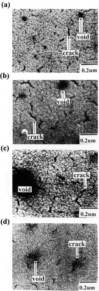
4.2. Effect of reactively sputter introduced nitrogen Figs. 7 and 8 show the surface morphology for the as-deposited and N2pre-sintered samples A's and samples B's,
respectively. As shown in Fig. 7a, there were cracks and voids on the surface of sample AAS. On the other hand,
sample BAS revealed a shiny and smooth surface, as
shown in Fig. 8a. The defects presented on the surfaces of the as-deposited CrZO layers were presumably due to volume expansion of the Cr layer by oxygen absorption as well as the stress mismatch between the CrZO and the Cu layers [16,17]. For the CrZNZO layer of sample B, nitro-gen was incorporated during the reactive sputter deposition [3,5]. Fig. 9 illustrates the XPS spectrum of N1s photoelec-trons in the CrZNZO layers. It showed that the N1s photo-electrons were present in elemental as well as nitride (Cr2N)
state [18]. The nitrogen tended to decorate the grain bound-aries [3,15] as well as nitrify the CrZNZO layer; this resulted in CrZNZO layers of better compliance to accom-modate the mismatch induced by the stress existing between Cu and CrZNZO layers [1,3,16]. We expected that the nitrogen stuffed Cr nitride layer of sample BAS should
possess superior capability of resisting the diffusion of oxygen and of Cu, and thus possesses better resistance against Cu oxidation than the defected CrZO layer of sample AAS[3,6±13]. As we reported in Section 3, the
abil-ity of resistance against Cu oxidation of the as-deposited
Fig. 5. XRD spectra for the O2annealed CrZNZO/Cu/SiO2/Si (sample B):
(a) samples without N2pre-sintering treatment and (b) samples with N2
pre-sintering treatment at 5008C.
Fig. 6. SIMS depth pro®les for the 5008C O2annealed samples B's: (a)
sample without N2pre-sintering treatment (BAS500O) and (b) sample with
CrZNZO layers was actually 1508C higher than that of the as-deposited CrZO layers.
4.3. Effect of N2pre-sintering treatment
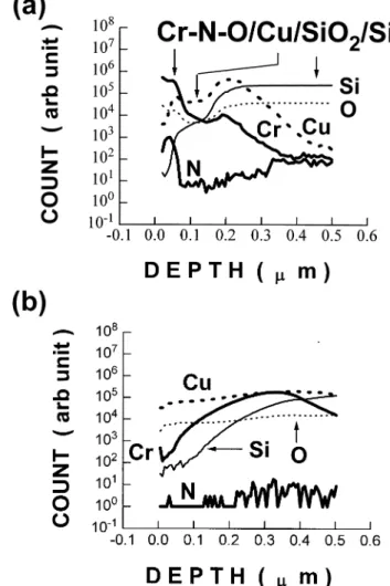
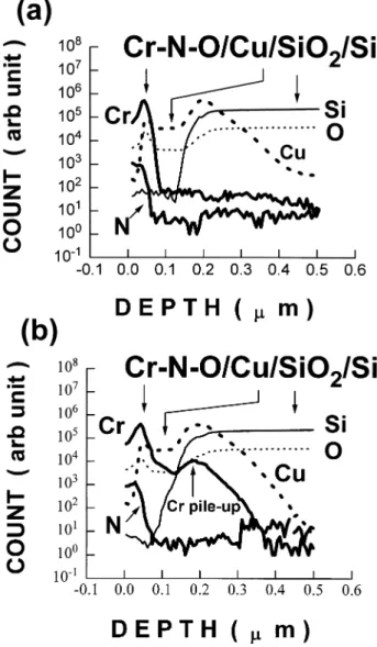
The comparison of SIMS depth pro®les between samples AAS and A5N and that between samples BAS and B5N are
illustrated in Figs. 10 and 11, respectively. For sample A, the N2 pre-sintering treatment resulted in nitrogen
incor-poration into the CrZO layer. However, the N2pre-sintering
treatment did not heal the inherent defects in the CrZO layer (Fig. 7b±d). Thus, the nitrogen incorporation in the CrZO layer did not improve the resistance against Cu oxidation because of the unhealed defects, i.e. cracking of the ®lms.
For sample B, however, the N2pre-sintering treatment did
not result in obvious change of the nitrogen pro®le. The SIMS depth pro®les of the compositional elements for the N2 pre-sintered sample B5N remained nearly the same as
those of the as-deposited sample BAS, except that the Cr
pro®le showed a pile-up at the Cu/SiO2interface (Fig. 11).
Pile-up of Cr at the Cu/SiO2interface was also observed for
the N2 pre-sintered sample A (Fig. 10). Moreover, the
surface morphology of sample B3Nlooked similar to that
of sample BAS, which was smooth and defect-free (Fig.
8a). Voids were found on the surface of samples B5Nand
B7N (Fig. 8b,c). The Cr pile-up at the Cu/SiO2 interface
indicated that Cr atoms diffused into/through Cu layer because the diffusivity of Cr in Cu ®lm is higher than that of Cu in Cr ®lm [15,16]. Presumably, the much more moved Cr led to coalescence of vacancies into void [17] on the surface of N2pre-sintered samples (Figs. 7 and 8). Besides,
the agglomeration of thin ®lms at elevated temperatures due to the mismatch of thermal expansion coef®cient between CrZNZO and Cu as well as the volume difference of Cr and Cr nitride might also contribute to the formation of voids. Moreover, grain growth of CrZNZO layers due to the high temperature N2 pre-sintering treatment resulted in shorter
diffusion paths for the oxidation species (i.e. Cu and oxygen), especially for the thin layers used in this study. Thus, Cu and oxygen diffused through these paths more easily, resulting in the degradation of the resistance against Cu oxidation for the N2pre-sintered samples.
From the data presented above, it is clear that N2
pre-sintering treatment caused degradation of the resistance against Cu oxidation for both CrZO and CrZNZO layers, though the pre-sintering temperature that would induce degradation was different for the CrZO and CrZNZO layers. It was 3008C for the former layer and was 5008C for the latter layer. As stated above, the inherent defect in samples A's was regarded as the major cause of this
differ-Fig. 7. SEM micrographs showing surface morphology of samples A's: (a) without N2pre-sintering treatment (AAS), (b) with N2pre-sintering
treat-ment at 3008C (A3N), (c) with N2pre-sintering treatment at 5008C (A5N) and
ence. The nitrogen stuffed Cr-nitride layers (sample B) were more compliant than the nitrogen de®cient CrZO layers (sample A). A much higher pre-sintering temperature was required for the CrZNZO layers to form void and grow their grains.
5. Summary and conclusion
This work studied the resistance against Cu oxidation of
sputter deposited CrZO and reactively sputter deposited CrZNZO layers of 200 AÊ thickness with and without
ther-Fig. 8. SEM micrographs showing surface morphology of samples B's: (a) without N2pre-sintering treatment (BAS), (b) with N2pre-sintering
treat-ment at 5008C (B5N) and (c) with N2pre-sintering treatment at 7008C (B7N).
Fig. 9. XPS spectrum showing the chemical states of N1s photoelectrons for the nitrogen incorporated in the CrZNZO layer.
Fig. 10. SIMS depth pro®les for samples A's: (a) without N2pre-sintering
mal N2pre-sintering treatment. The CrZO covered Cu ®lms
can resist thermal annealing in O2ambient at temperatures
up to 3508C, while the CrZNZO covered Cu ®lms can resist the same treatment at temperatures up to 5008C, all without causing Cu oxidation. The distinction of the resistance against Cu oxidation was presumably due to the inherent defects, including cracks and voids, in the CrZO ®lm, and the nitrogen doping in the CrZNZO ®lm. With N2
pre-sintering treatment on the CrZO or CrZNZO covered Cu ®lms, the resistance against Cu oxidation was degraded. The higher the N2pre-sintering temperature was, the lower the
oxidation temperature of Cu became. The unhealed defects of N2pre-sintered CrZO layers were presumed to be the
principal reason of degradation for the CrZO case. On the other hand, voids formation after N2pre-sintering treatment
at elevated temperatures was regarded as the cause of
degra-dation for the CrZNZO case. Nitrogen in the CrZNZO layers decorated the grain boundaries of Cr nitride and improved the surface morphology of the layers, resulting in a better resistance against Cu oxidation than that of the CrZO layer. Since the bene®cial effect of nitrogen doping may be outweighed by the formation of voids during the N2
pre-sintering process, we conclude that the N2pre-sintering
treatment is an excess thermal treatment, and should be avoided in the application of CrZO or CrZNZO ®lm as resistant layer against Cu oxidation.
Acknowledgements
The authors wish to thank the Semiconductor Research Center of National Chiao-Tung University for providing excellent processing environment. This work was supported by the National Science Council, ROC, under contract no. NSC-86-2215-E-009-040.
References
[1] Copper-based Metallization and Interconnects for Ultra-Large-Scale Integration Applications (special issue), Thin Solid Films 262 (1995). [2] J.D. McBrayer, R.M. Swanson, T.W. Sigmon, J. Electrochem. Soc.
133 (1986) 1242.
[3] S.Q. Wang, S. Suthar, C. Hoe¯ich, B.J. Burrow, J. Appl. Phys. 73 (1993) 2301.
[4] J. Li, J.W. Mayer, E.G. Colgan, J. Appl. Phys. 70 (1991) 2820. [5] C.-K. Hu, B. Luther, F.B. Kaufman, J. Hummel, C. Uzoh, D.J.
Pear-son, Thin Solid Films 262 (1995) 84.
[6] W.A. Lanford, P.J. Ding, W. Wang, S. Hymes, S.P. Murarka, Thin Solid Films 262 (1995) 234.
[7] P.J. Ding, W. Wang, W.A. Lanford, S. Hymes, S.P. Murarka, Appl. Phys. Lett. 65 (1994) 1778.
[8] J. Li, J.W. Mayer, Y. Shacham-Diamand, E.G. Colgan, Appl. Phys. Lett. 60 (1992) 2983.
[9] H. Itow, Y. Nakasaki, G. Minamihaba, K. Suguro, H. Okano, Appl. Phys. Lett. 63 (1993) 934.
[10] D.S. Gardner, J. Onuki, K. Kudoo, Y. Misawa, Q.T. Vu, Thin Solid Films 262 (1995) 104.
[11] Y. Igarashi, T. Yamanobe, T. Yamaji, S. Nishikawa, T. Ito, Jpn. J. Appl. Phys. 33 (1) (1994) 462.
[12] S. Hymes, S. P. Murarka, C. Shepard, W.A. Lanford, J. Appl. Phys. 71 (1992) 4623.
[13] P.J. Ding, W.A. Lanford, S. Hymes, S.P. Murarka, J. Appl. Phys. 74 (1993) 1331.
[14] W. Kern, D.A. Puotinen, RCA Rev. 31 (1970) 187.
[15] E.A. Brandes, Smithells Metals Reference Book, 6th ed., Robert Hart-noll, Bodmin, 1983, pp. (8±21)± (8±25).
[16] D.R. Lide (Ed.), CRC Handbook of Chemistry and Physics, 73rd ed., CRC Press, Boca Raton, Florida, 1992, Section 12: Properties of Solids.
[17] R.E. Reed-Hill, Physical Metallurgy Principles, 2nd ed., Van Nostrand, New York, 1972, pp. 386±390.
[18] G.E. Muilenberg (Eds.), Handbook of X-ray Photoelectron Spectro-scopy, Perkin-Elmer Corporation, Physical Electronics Division, Eden Prairie, Minnesota, 1979.
Fig. 11. SIMS depth pro®les for samples B's: (a) without N2pre-sintering