行政院國家科學委員會專題研究計畫 成果報告
低雜訊與低耗功率之 CMOS 射頻元件與電路技術
計畫類別: 個別型計畫
計畫編號: NSC92-2218-E-009-024-
執行期間: 92 年 11 月 01 日至 93 年 07 月 31 日
執行單位: 國立交通大學電子工程學系
計畫主持人: 郭治群
報告類型: 精簡報告
報告附件: 出席國際會議研究心得報告及發表論文
處理方式: 本計畫涉及專利或其他智慧財產權,1 年後可公開查詢
中 華 民 國 93 年 12 月 8 日
低雜訊與低消耗功率之射頻 CMOS 元件與電路技術
Low Noise and Low Power RF CMOS Device and
Circuit Technology
計 畫 編 號 : N S C 9 2 - 2 2 1 8 - E 0 0 9 - 0 2 4
執 行 期 間 : 9 2 年11 月0 1 日 至 9 3 年0 7 月3 1 日
執 行 單 位 : 國立交通大學
計畫主持人: 郭治群
中文摘要 本計畫重點為低雜訊與低秏功率射頻積體電路技術 之研究開發。探討新的電路架構與操作方法,以達 低秏功 率之目標。低雜 訊放大器 (LNA)與混頻器 (mixer)為兩個主要研究對象,其秏功率規格訂為 LNA+mixer<10mW,應用範圍為 5.2~5.8GHz 之無線 通訊。本計畫取得台積電 R&D 的 support,利用其 0.13 微米射頻 CMOS 製程技術,已於今年二月順利 tape out 一 4mm*4mm 的 test chip,其中包括兩個新 的 電 路 架 構 : CMOS cascode 與 transformer degeneration,以及一組創新的 test key,作為射頻 CMOS model 開發之用。有關 LNA 之設計,常用的 方法為 inductor degeneration 以降低其雜訊,但根據 電路模擬結果,我們發現,電感本身的電阻就會貢 獻額外的雜訊,noise figure 可能多出約 1dB。此外, lossy pad 和 lossy substrate 為兩個重要的雜訊來源, 對於小元件而言,其影響非常顯著。本計畫已開發 一套創新的 transmission-line de-embedding 的方法, 可正確地萃取射頻 CMOS 元件本身的雜訊並作雜訊 模型開發之基礎。此套方法已在 0.13 微米元件上得 到驗証,其擷取出之雜訊值與 noise correlation matrix 計算而得者相當吻合。有關 mixer 之設計,線性度之 改善特別重要,但在兼顧低秏功率之條件下,為一 相當具挑戰之課題。本計畫參考文獻加上詳盡的電 路模擬分折結果,已設計一套 multi-gated 元件結構, 並已 tape-out 至 CiC,利用台積電 0.18 微米製程技術 來 驗 証 我 們 的 模 擬 結 果 , 目 標 為 IM3 可 降 低 10dBm(射頻訊號功率為-35dBm~-20dBm ) 關鍵詞 : 低秏功率,射頻金氧墜電晶體,雜訊,線性度Abstract —In this project, we explore the new circuit
topologies and operation schemes to achieve low
power RF CMOS IC targeting applications on 5.2~5.8GHz wireless communication. LNA and mixer are two major circuit elements of our focus and the performance target is set as LNA+mixer total power < 10mW by using 0.13G CMOS technology with supply voltage at 1.2V. CMOS cascode and transformer degeneration are two new topologies that have been implemented in a test chip. Besides the new circuit architectures, new test structures for RF CMOS modeling have been designed and implemented in the same test chip with support from tsmc R&D in terms of tape-out, mask making, and wafer processing. To achieve low noise for LNA, impedance matching by using inductance degeneration is generally used but extra noise arising from the non-ideal inductor is suggested by simulation. The non-zero series resistance associated with the existing inductors will contribute noise figure of near 1dB. Lossy pads and lossy substrate are identified as two key factors introducing extra noise to intrinsic CMOS, particularly for the smaller devices with fewer finger numbers. A novel transmission line de-embedding method is developed for accurate RF CMOS noise extraction and modeling. The extracted minimum noise figure (NFmin) after de-embedding matches well
with the published noise correlation matrix method but is relatively simple without resort to the complicated matrices calculation. Regarding the linearity of special concern for mixer, a new linearization technique using 2nd harmonic termination by multi-gated structure has been justified by simulation and implemented by test key tape-out to CiC adopting tsmc 0.18um RF CMOS process. The IM3 can be suppressed by around 10dBm at RF power of –20~-35dBm and maintain the same DC power.
Key words : Low power RF CMOS, noise, linearity,
Background and Objective
Wireless communication and mobile phones are
among the numerous applications of RF ICs to drive
the features of low power, low noise, small form factor, and low cost. Submicron CMOS technology is
recognized with great potential for
RF front-end at GHz era attributed to its advantages of low voltage, high speed, high integration, and low cost. LNA and mixer are two most frequently used RF circuits adopting CMOS devices. Both circuits include active transistors and passive elements like inductors, capacitors, and resistors. The major challenges lie in the trade-off among various performance parameters such as NF (noise figure), IIP3 (third order intercept
points representing the linearity), P1dB (1 dB
compression), power gain (Ga), power dissipation,
reverse isolation (S12), input/output return loss, and
stability factor, etc. Contradiction exist between some parameters by nature, e.g. the lower noise paid the penalty of higher power dissipation, the better matching led to higher noise, etc. Of these parameters the trade-off between dissipated power and the dynamic range is the critical concern for low-power RF circuits. For MOSFET devices, low power dissipation requires low supply voltage and low drain current, while large dynamic range necessitates large transconductance and large effective gate voltage (defined as Vgs-VT) [1][2]. Roughly conforming to
square law, however, the bias current in saturation is linked to the product of the latter two quantities, which sets a fundamental constraint on low-power circuit design. In tuned circuits such a constraint can be relaxed if appropriate circuit architecture is chosen, e.g. improvement of linearity by reactive degeneration without degradation of noise performance [3]. In this project power-conscious design for RF front-end circuits is to be implemented by taking the advantage of scaling technology in both passive components and active devices. For passive components, high quality factor is the key to low power design to achieve the same level of noise and gain performance. For example, the loss of an inductor in the input matching network and the output loading for a LNA circuit causes high power consumption to compensate for the loss. The quality factor of on-chip inductors is hardly larger than 15. In recent years extensive effort has been focused on improvement of quality factor for on-chip inductors [4, 5]. Advanced process technology offers better material of metal lines and thicker metal
layer that result in lower resistivity due to metal lines and skin effect. Besides, it occurs that advanced technology offers more metal layers that increase the flexibility in design of better structures. New structures will be investigated for high-quality inductors. For active devices, scaling of channel length dramatically raises up the cut-off frequency (fT)
such that power consumption can be lowered down with acceptable trade-off of other parameters [6]. The development of CMOS devices has made it competitive to bipolar devices for applications in radio frequency circuits. Most published work, however, is still applying only NMOS devices in circuit design for its higher fT than that of PMOS devices. As PMOS
devices are applicable to radio frequency operation, circuit design can benefit in the topology of complementary circuits. The concept of current reuse in such kind of CMOS circuits has been published [7]. This concept can be extended further for low power design. The mentioned issues cannot be solved just by device tuning but new circuit architectures are considered the “must” approaches to achieve the true solution. Novel circuit architectures accompanied with device technology advancement is recognized as the right way to go. Regarding LNA and mixer, different circuit topologies such as single-ended and differential pair accompanied with single stage or cascode structure, degeneration by inductor or transformer, capacitively coupled LC tank or decoupling by transformer, pure nMOS or complementary pair by nMOS/pMOS, etc. have been verified by simulation to investigate different flavors of circuit topology. Among the mentioned topologies, transformer degeneration and CMOS cascode have been implemented on the test chip taped out through support of tsmc R&D using 0.13G RF CMOS process.
Results and Discussion
A. New Circuit Topologies for Low Power and Low Noise LNA – CMOS cascode and Transformer Degeneration
CMOS cascode is a new circuit topology proposed to increase the amplifier transconductance without increasing the power dissipation [8]. Current reuse technique by CMOS structure at the input stage is adopted and verified by simulation. Fig.1 shows the circuit topology that we have implemented through 0.13µm RF CMOS tape-out in which passive elements of inductors and capacitors are used for impedance
matching, e.g. Lg, Ls1, and Ls2 for input impedance
matching while Lf, Cb1, and Cb2 for output impedance
matching. Table 1. demonstrates the performance calculated by simulation using tsmc 0.13µm RF CMOS model. All the key parameters as listed can meet the spec. quite well. It’s worthy of mention that
NFmin can be maintained as low as 1.8dB and power
dissipation can be reduced below 5mW.
Fig. 1. CMOS cascode circuit scheme for LNA
Table 1. Simulation Results and Spec. for Low Power LNA using CMOS cascode topology
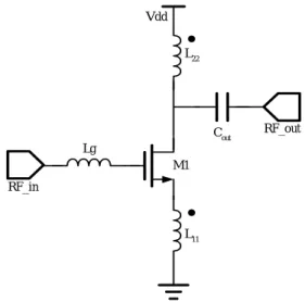
As mentioned previously that cascode configuration is the most widely used topology for CMOS LNA, particularly for those reported to date for 5GHz wireless LANs. However, the two-transistor stack sets constraint on supply voltage scaling. On-chip transformer degeneration was proposed to provide reactive negative feedback to neutralize the Miller capacitance Cgd while maintain low Vdd [9]. Fig.2
illustrates the circuit topology of a single-end LNA
adopting transformer degeneration in which feeding back a portion of the output signal via the transformer can effectively cancel the feedback from output to input through the Miller capacitance and neutralize the amplifier. The magnetic coupling between input and output using a transformer adds negative feedback, which can be appreciated by applying a small positive test voltage at node RF_IN. The increased drain current
lowers RF_out or equivalently, increases the ac voltage
drop across L22. The voltage across L11 also increases
but in the opposite direction due to inverting wire configuration. On-chip inductor Lg is employed at gate
to achieve input impedance matching while Cout is
adopted at drain to realize output impedance matching. Table 2. shows the performance calculated by ADS simulation in which ADS momentum is employed to simulate the transformer characteristics. Device layout size and bias conditions are fine tuned to achieve the optimized performance. It’s demonstrated that Vdd as
low as 0.8V can achieve low power at 4mW and maintain sufficient gain at 12dB and low noise, NFmin
<2dB. Si verification will be done after tsmc 0.13µm RF CMOS wafer out.
RF_in RF_out Lg L11 M1 Cout Vdd L22
Fig. 2. Single-end LNA with transformer degeneration
Cp Ls1 Ls2 Lg Lt Ct Lf Cb1 Cb2 項目 模擬結果 規格 製程 TSMC CMOS 0.13um TSMC CMOS 0.13um
DC Supply Voltage 1.2V 1.2V S21 14.6dB >14dB S12 -20.9dB <-20dB S11 -14.3dB <-13dB S22 -24dB <-22dB Noise Figure (NFmin) 1.8dB <2dB
dB
P−1 -20.4dBm >-22dBm
IIP3 -10.3dBm >-11dBm
Power Dissipation 4.5mW <5mW
Performance(項目) Simulation Target(規格) Process TSMC 0.13µm (G) RF CMOS DC Supply Voltage 0.8V 0.8V Gain 12dB >10dB Noise Figure 1.98dB < 2.5dB
Input return loss -12.2dB <-10dB Output return loss -29.2dB <-10dB P-1dB -4.4dBm >-10dBm IIP3 Power Dissipation 4mW < 5mW
Table 2. Simulation results and spec. for low power LNA using transformer degeneration
B. New Circuit Topologies for Low Power and High Linearity LNA & Mixer – Multi-gated Transistor
The integration of LNA, mixer, and driver amplifier on a single –chip is becoming a reality by using RF CMOS technology. Due to the fact, the linearity requirement per DC power is getting stringent. To meet the spec. of linearity with minimum power, new linearization techniques with low power are demanded. Topology of multi-gated transistors is proposed to improve the linearity (IIP3, IM3) by 2
nd
harmonic termination technique [10-11]. Fig. 3 indicates the topology of multi-gated common transistors that we have taped out to CiC for Si implementation and verification. gm” cancellation is
the major concept to suppress IM3 and improve IIP3.
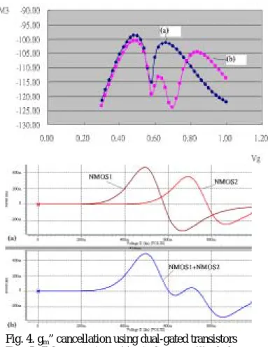
Fig. 4 shows the simulation result of gm” cancellation
using dual-gated transistors with optimized gate bias offset and transistor widths. Regarding the
suppression of IM3 of our major concern, Fig. 5
demonstrates the improvement by 10~20dB can be achieved under operation at 5.5GHz and RF power of –35dBm.
Fig. 3. The schematics of multi-gated transistors
Fig. 4. gm” cancellation using dual-gated transistors
Fig. 5 IM3 comparison (a) single gate (2) dual-gate
transistor scheme (RF power is –35dBm)
Table 3. demonstrates the simulation results and comparison with the spec. for nonlinearity and noise figure
C. Novel Test Structures for RF CMOS Parameter Extraction and Accurate Modeling
It has been well recognized that design of RF device test structure plays a critical role in accurate parameter extraction and modeling. De-embedding technique cannot eliminate all the parasitics existing on chip, particularly true for lossy pad and lossy substrate effect on noise. In this project, we have created a full set of test key incorporating 4 categories 16 1 = nr NMOS 12 2 = nr NMOS 1 D D2 1 G G2 2 S 1 S 1 g V 2 g V
third order intermodulation distortion 改善量值 @5.5GHz & V vgs≈0.6~0.74 Noise Figure 增加量 @5.5GHz & vgs≈0.6~0.74V 模擬結果 10dB ~ 20dB -0.25dB ~ 0.35dB 預計規格 8dB ~ 15dB < 0.5dB
of novel test structures to facilitate accurate parameter extraction, decoupling, and RF CMOS modeling. This set of test key has been taped out through support of tsmc R&D. The 4 categories of test structures are summarized in table 4.
Table 4
Test Structures Objectives Layout PO on STI/CT on OD Extraction/decoupling/modeling of (Rg,Rch), (Cgs,Cgd, Cif,ect.) NF PO .S.4 CO.S.3 Branch substrate CT
Extraction/modeling ofRsub, CsubNF NF,branch
Narrow OD branch
Extraction/modeling of narrow width effect on fT, fmax, NFmin
OD width, space
NMOS/CMOS cascode
Optimized low noise structure for LNA
Common/shared OD
Conclusion
Two new circuit topologies for low power and low noise CMOS LNA (CMOS cascode and transformer degeneration) have been implemented and taped out through tsmc R&D using 0.13µm RF CMOS technology. The circuit performance can meet spec. in terms of power, noise, and isolation by simulation using current version of tsmc 0.13µm RF CMOS model. Besides, a set of novel test key for accurate parameter extraction and modeling has been implemented and taped out along with the circuits to go through tsmc 0.13µm RF CMOS process. One new topology named as multi-gated transistor for linearity improvement has been implemented and taped out to CiC to go through tsmc 0.18µm RF CMOS process. On chip test and verification will be done to study the created new circuit topologies and the novel test key for modeling.
References
[1] A. A. Abidi, “High Frequency Noise Measurements on FET’s with Small Dimensions,” IEEE Trans. Electron Devices, vol. ED-33, pp. 1801-1805, 1986. [2] Q. Huang, F. Piazza, P. Orsatti, and T. Ohguro, ”The
Impact of Scaling Down to Deep Submicron on CMOS RF Circuits,” IEEE JSSC, vol. 33, no. 7, pp. 1023-1036, 1998.
[3] A. A. Abidi, G. J. Pottie, and W. J. Kaizer, “Power-Conscious Design of Wireless Circuits and Systems,” Proc. Of the IEEE, vol. 88, no. 10, Oct. 2000.
[4] C. P. Yeu and S. S. Wong, “On-Chip Spiral Inductors with Patterned Ground Shields for Si-Based RF IC’s,”
IEEE JSSC, Col. 33, No. 5, May 1998.
[5] C.-C. Tang, C.-H. Wu, and S.-I. Liu, “Miniature 3-D Inductors in Standard CMOS Process,” IEEE JSSC, Vol. 37, No. 4, Apr. 2002.
[6] D. K. Shaeffer, and T. H. Lee, “A 1.5-V, 1.5-GHz CMOS Low Noise Amplifier,” IEEE JSSC, vol. 32, No. 5, May 1997.
[7] A. N. Karanicolas, “A 2.7-V 900-MHz CMOS LNA and Mixer,” IEEE JSSC, vol. 31, No. 12, Dec. 1996 [8] H. Fouad, K. Sharaf, E. El-Diwany, H. El-Hennawy, “An RF CMOS cascode LNA with current reuse and inductive source degeneration”, Circuits and Systems, 2001. MWSCAS 2001. Proceedings of the 44th IEEE 2001 Midwest Symposium on , Volume: 2 , 14-17 Aug. 2001
Pages:824 - 828 vol.2
[9] Cassan, D.J.; Long, J.R.;” A 1-V
transformer-feedback low-noise amplifier for 5-GHz wireless LAN in 0.18um CMOS,” IEEE Journal Solid-State Circuits, vol.38, Issue: 3 , 2003 p.427 – 435
[10] Tae Wook Kim; Bonkee Kim; Kywro Lee,“Highly Linear RF CMOS Amplifier and Mixer Adopting MOSFET Transonductane Linearization by Multiple Gated Transistors” IEEE Symposium,pp.107-110, June 2003 “” [11] Bonkee Kim; Jin-Su Ko; Kwyro Lee ,“A New
Linearization Technique for MOSFET RF Amplifier Using Multiple Gated Transistors” Microwave and Guided Wave Letters ,IEEE,pp.371-373, Sept. 2000 “”