低雜訊與低耗功率之CMOS射頻元件與電路技術
全文
數據
相關文件
The major testing circuit is for RF transceiver basic testing items, especially for LNA Noise Figure and LTE EVM test method implement on ATE.. The ATE testing is different from
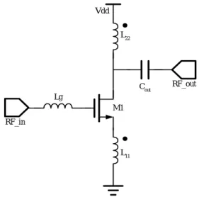
傳統的 RF front-end 常定義在高頻無線通訊的接收端電路,例如類比 式 AM/FM 通訊、微波通訊等。射頻(Radio frequency,
Due to low birth rate and setting up many new senior high schools and senior vocational schools, now the rate of entering a higher school for junior high school graduates has
Sugii, “Junction profile engineering with a novel multiple laser spike annealing scheme for 45-nm node high performance and low leakage CMOS technology,” in IEDM
First we explain how to implement CMOS current-mode quadratic circuits and design the proposed circuit in the way of multiple corrections.. We use the best
Bluetooth:為一低成本、低耗電、近距離的無線通訊技術,每個 裝置有一個唯一的 48-bit 位址,其網路容量可達 8 個 Bluetooth 裝置已 Peer-to-Peer 或
The proposed circuit is based on CMOS Current-Mode Quadratic Function Circuits, its W/L ratio and construction could be adjusted by the relative error that the users
“Feasibility of Using W/TiN as Metal Gate for Conventional 0.13 µm~ CMOS Technology and Beyond” in IEDM Tech. Misra, “Effect of the composition on the electrical properties
