氮化鎵異質結構場效電晶體
159
0
0
全文
(2) 氮化鎵異質結構場效電晶體 GaN-based Heterostructure Field Effect Transistors 研 究 生 :李 建 騏 指導教授 :李 建 平 博 士. Student : Chien-Chi Lee Advisor : Dr. Chien-Ping Lee. 國 立 交 通 大 學 電子工程學系電子研究所 博 士 論 文 A Dissertation Submitted to Department of Electronics Engineering College of Electrical Engineering and Computer Science National Chiao Tung University in Partial Fulfillment of the Requirements for the degree of Doctor of Philosophy in Electronics Engineering June 2004 Hsinchu, Taiwan, Republic of China. 中華民國九十三年六月.
(3) 氮化鎵異質結構場效電晶體 學生:李建騏. 指導教授:李建平 博士 國立交通大學 電子工程系 電子研究所. 摘 要. 本論文的研究目標為開發高性能氮化鎵場效電晶體。研究課題包括元件製程技術的 開發及元件基本問題的探討。在元件製程技術的開發部份,我們成功的開發出製作氮化 鎵場效電晶體所需的製程技術。這些製程技術包括電感偶合電漿蝕刻、電漿處理的低阻 值歐姆接觸及窄T型閘極製作。在電感偶合電漿蝕刻部分,在適當的蝕刻條件下,我們 可以製作出具有平坦及垂直側壁的絕緣平台。在元件歐姆接觸部分,我們利用不同條件 的電漿處理得到低阻值的歐姆接觸 (~ 1×10⁻⁶ Ω⋅cm2)。此外,我們也進一步證明其具有 很好熱穩定性。在窄T型閘極製作部份,我們利用低加速電壓的電子束來製作窄T型閘。 我們設計適當的圖形來有效地改善低加速電壓下的正向散射效應,最小的閘極長度可縮 小至40 nm。 在元件基本問題的探討部分,我們研究元件的極化效應及熱效應。在元件的極化效 應部分,我們做了廣泛的研究。我們設計幾種不同的元件結構,探討其表面型態、電子 傳輸性質及元件特性,並實驗證明極化效應對電子傳輸性質及元件特性皆扮演了關鍵性 的角色。對於undoped結構,極化效應可導致高濃度二維電子氣 (~ 1×1013 cm-2) 在 AlGaN/GaN界面形成。因此AlGaN/GaN元件具有很大的輸出電流。在元件的熱效應部 分,我們探討在不同溫度下,不同的元件結構其通道中電子的傳輸性質及元件特性。我 i.
(4) 們利用活化能的分析,成功的解釋調變摻雜結構的元件在不同的溫度下通道中電子濃度 變化的原因。此外,我們也對不同結構的元件在不同的溫度下的特性作比較,並觀察到 具調變摻雜結構的元件在不同的溫度下的特性都比undoped結構的元件好。我們成功的 製作出具有大輸出電流 (undoped ~ 700 mA/mm; modulation-doped ~ 1000 mA/mm)、高 崩潰電壓 (undoped ~ 100 V; modulation-doped ~ 53 V) 及高操作頻率 (undoped ~ 32 GHz; modulation-doped ~ 75 GHz) 的氮化鎵場效電晶體。這些優異的元件特性也充分的 證明氮化鎵異質結構場效電晶體的確是非常好的微波高功率元件。. ii.
(5) GaN-based Heterostructure Field-Effect Transistors Student: Chien-Chi Lee. Advisor: Dr. Chien-Ping Lee. Department of Electronics Engineering & Institute of Electronics National Chiao Tung University. Abstract In this dissertation, we investigated AlGaN/GaN heterostructure field-effect transistors (HFETs) to develop high-performance AlGaN/GaN HFETs. The research topics cover the development of basic device processing technologies and fundamental device issues. We successfully developed the technologies required for the fabrication of high-performance AlGaN/GaN HFETs, including the ICP etching of GaN, low resistance ohmic contacts to n-GaN and the narrow T-gate fabrication. A proper etching rate together with the vertical sidewall profile and smooth surface can be obtained in the ICP etching of GaN. Plasma-treated ohmic contacts exhibit low contact resistances (~ 1×10⁻⁶ Ω⋅cm2) and excellent thermal stability. A low accelerating voltage of 15 kV was used to perform the narrow T-gate fabrication. With the specially designed writing patterns, the forward scattering effects associated with a low accelerating voltage can be effectively improved. Narrow T-gates with the foot width of 40 nm were obtained. In addition, we studied the polarization effect and the thermal effect of AlGaN/GaN HFETs. The polarization effect plays a crucial role in both the electron transport properties and device characteristics of AlGaN/GaN HFETs. The strong polarization effect in the undoped AlGaN/GaN heterostructures leads to the formation of high-concentration 2DEG at iii.
(6) the AlGaN/GaN interface (~ 1×1013 cm-2) and thus large output current can be obtained. The thermal effect is particularly important for the high-temperature application of devices. We found that in addition to the commonly known problem in the thermal conductivity of substrate, the device structure also plays a significant role in the temperature-dependent electron transport properties and the high-temperature performance of the device. Furthermore, we successfully fabricated high-performance submicron AlGaN/GaN HFETs. Both the undoped and the modulation-doped Al0.3Ga0.7N/GaN HFETs exhibited very high output currents (undoped ~ 700 mA/mm; modulation-doped ~ 1000 mA/mm), high breakdown voltages (undoped ~ 100 V; modulation-doped ~ 53 V) and high cut-off frequencies (undoped ~ 32 GHz; modulation-doped ~ 75 GHz). These excellent device characteristics obtained experimentally demonstrated that AlGaN/GaN HFETs are indeed excellent high power devices operating at high frequencies.. iv.
(7) Acknowledgements. 首先,非常感謝我的指導教授-李建平博士。和老師討論問題是很有趣的,雖然有 時讓人倍感壓力。此外,老師非常尊重每個學生的興趣,給予寬廣的學習空間並鼓勵大 家積極研究創新。I like such style. 其次,非常感謝一起參與研究工作的夥伴。我的學弟-葉孟欣及石正楓,及提供磊 晶試片的朋友們- 連威磊晶曾堅信博士及郭正達博士,以及工研院光電所祁錦雲主任、 涂如欽博士及卓昌正博士。你們的貢獻很大。因為你們的熱心參與,我們的研究工作才 能順利的來推動。 再來,非常感謝MBE實驗室的全體成員,包括已畢業的或在學的學長、學弟及學妹 們。你們的貢獻也很大。你們是我在學習上的好夥伴及生活上歡樂的泉源。此外,交大 奈米中心及國家奈米元件實驗室在實驗設備上的提供,更是不可或缺的要素。 最後,非常感謝家人的支持及鼓勵。你們是我的最終的依靠。. v.
(8) Contents. Abstract (Chinese). i. Abstract (English). iii. Acknowledgement. v. Contents. vi. Table captions. x. Figure captions. xii. Chapter 1 Introduction. 1. 1-1 Overview and research motivation. 1. 1-2 Thesis organization. 4. References. 5. Chapter 2 GaN-based materials and heterostructure field-effect transistors. 6. 2-1 Fundamental material properties of GaN. 6. 2-2 Polarization effect. 8. 2-2-1 Crystal structure and polarity. 8. 2-2-2 Spontaneous and piezoelectric polarizations. 9. 2-2-3 Strain relaxation. 13. 2-2-4 Sheet charge concentration of 2DEG. 14. 2-3 AlGaN/GaN HFETs. 15. 2-3-1 Important issues in the growth of AlGaN/GaN heterostructures. 16. 2-3-2 Device operation principle. 17. 2-3-3 Device fabrication. 17. vi.
(9) References. 19. Chapter 3 Inductively coupled plasma etching of GaN. 28. 3-1 Introduction. 28. 3-2 Experiment. 29. 3-3 Results and discussion. 29. 3-3-1 Ni mask fabrication. 29. 3-3-2 ICP etching. 30. 3-4 Conclusion. 32. References. 34. Chapter 4 Low resistance Ohmic contact to n-GaN. 43. 4-1 Introduction. 43. 4-2 Experiment. 44. 4-3 Results and discussion. 45. 4-3-1 Plasma treatments. 45. 4-3-2 Thermal stability issue. 48. 4-3-3 Forming gas ambient treatments. 50. 4-4 Conclusion. 51. References. 53. Chapter 5 Narrow T-gate fabrication on GaN. 64. 5-1 Introduction. 64. 5-2 Experiment. 65. 5-3 Results and discussion. 66. vii.
(10) 5-3-1 Writing pattern design. 66. 5-3-2 40 nm narrow T-gate frbrication. 66. 5-4 Conclusion. 69. References. 70. Chapter 6 Polarization effect in AlGaN/GaN HFETs. 75. 6-1 Introduction. 75. 6-2 Experiment. 76. 6-3 Results and discussion. 78. 6-3-1 Surface morphology. 78. 6-3-2 Electron transport properties. 79. 6-3-3 Device characteristics. 84. 6-4 Conclusion. 88. References. 90. Chapter 7 Thermal effect of AlGaN/GaN HFETs. 107. 7-1 Introduction. 107. 7-2 Experiment. 108. 7-3 Results and discussion. 110. 7-3-1 Electron transport properties. 110. 7-3-2 Device high-temperature performance. 113. 7-4 Conclusion. 118. References. 120. Chapter 8 Conclusion and proposed future work. 130. viii.
(11) 8-1 Conclusion. 130. 8-2 Proposed future work. 131. References. 133. Vita. 136. Publication list. 137. ix.
(12) Table captions Chapter 2 Table 2-1 Fundamental material properties of several important semiconductors [1]. Table 2-2 Structural properties of GaN-based materials, sapphire and SiC substrates. Table 2-3 Spontaneous polarization, piezoelectric and dielectric constants of AlN, GaN and InN [5].. Chapter 3 Table 3-1 Etching condition where the Ar flow rate was modulated. Table 3-2 Etching condition where the bias power was modulated. Table 3-2 Etching condition where the Cl2 flow rate was modulated.. Chapter 4 Table 4-1 Etching conditions and TLM data. Table 4-2 The conditions of the plasma treatment.. Chapter 8 Table 8-1. A comparison on the device performance of AlGaN/GaN HFETs on sapphire substrates. x.
(13) Table 8-2. A comparison on the device performance of AlGaN/GaN HFETs on SiC substrates.. xi.
(14) Figure captions Chapter 2 Fig. 2-1 Schematic diagrams of the crystal structure and the polarity of the Ga-face and N-face GaN crystals [5]. Fig. 2-2 Polarization-induced sheet charge and directions of the spontaneous and piezoelectric polarization in the Ga-face and N-face strained and relaxed AlGaN/GaN heterostructures [5]. Fig. 2-3 Critical thickness of AlGaN grown on relaxed GaN calculated using the models of Matthews and Blakeslee or Fischer et al. as a function of Al composition. AlGaN layers with different thickness and Al composition grown pseudomorphically on GaN by MOCVD and MBE are marked by black symbols. Partially relaxed AlGaN layers (white symbols) are separated from the pseudomorphic heterostructures by a dash line [7]. Fig. 2-4 Calculated total polarization induced sheet charge for pseudomorphically grown AlGaN/GaN heterostructures under different degree of relaxation and Al compositions [7]. Fig. 2-5 Calculated maximum sheet carrier concentration for pseudomorphic (dashed lines) and partially relaxed (solid lines) Ga-face AlGaN/GaN heterostructures with a barrier thickness of 200 Å [7]. xii.
(15) Fig. 2-6 The schematic diagram of typical AlGaN/GaN heterostructure field-effect transistors. Fig. 2-7 The process procedures for the fabrication of AlGaN/GaN HFETs.. Chapter 3 Fig. 3-1 Optical microscope (OM) images of the Ni metal masks. This is done after lift-off process was performed. Fig. 3-2 Optical microscope (OM) images of the Ni metal mask, where the black parts represent the etched Ni mask and the outer transparent parts represent photoresists. This is done by wet etching process. Fig. 3-3 Etching rates under different Ar flow rates. Fig. 3-4 SEM images of the sidewall profile after ICP etching was performed under different Ar flow rates. Fig. 3-5 Etching rate under different bias powers. Fig. 3-6 SEM images of the sidewall profile after ICP etching was performed under different bias power. Fig. 3-7 Etching rate under different Cl2 flow rate. Fig. 3-8 SEM images of the sidewall profile after ICP etching was performed under different Cl2 flow rates.. xiii.
(16) Chapter 4 Fig. 4-1 Current-voltage characteristics of the as-deposited ohmic contacts treated with Ar plasma at different Ar flow rate. Fig. 4-2 The dependence of contact resistance and specific contact resistance of the as-deposited ohmic contacts on Ar flow rate. Fig. 4-3 Current-voltage characteristics of the alloyed ohmic contacts under different Ar flow rate. Fig. 4-4 The dependence of contact resistance and specific contact resistance of the alloyed ohmic contacts on Ar flow rate. Fig. 4-5 Current-voltage characteristics of the as-deposited ohmic contacts under different Ar treatment time. Fig. 4-6 Current-voltage characteristics of the alloyed ohmic contacts under different Ar treatment time. Fig. 4-7 The dependence of contact resistance and specific contact resistance of the alloyed ohmic contacts on Ar treatment time. Fig. 4-8 Aging test results of contact resistance in N2 ambient for samples with Cl2/Ar. plasma treatment. Fig. 4-9 Aging test results of specific contact resistance in N2 ambient for samples with Cl2/Ar plasma treatment. xiv.
(17) Fig. 4-10 Aging test results of specific contact resistance in N2 ambient for samples with Ar plasma treatment. Fig. 4-11 Aging test results of specific contact resistance in air ambient. Fig. 4-12 Current-voltage characteristics of the ohmic contacts annealed in forming gas ambient. Fig. 4-13 A comparison of specific contact resistance of the ohmic contacts annealed in N2 gas and in forming gas ambient.. Chapter 5 Fig. 5-1 The schematic of the writing pattern layout designed for narrow T-gate fabrication. Fig. 5-2 The average footwidth of narrow T-gates as a function of the central dose. The average footwidth is 50 nm. Fig. 5-3 The resist profile after development. A very good undercut profile and a narrow foot opening with dimensions of about 60 nm were obtained. Fig. 5-4 A 40 nm narrow T-gate on a GaN substrate after metal deposition and lift-off.. Chapter 6 Fig. 6-1 The schematic of undoped structure (sample No. 1), where Al composition is 0.17 and the top AlGaN layer thickness is 18 nm. xv.
(18) Fig. 6-2 The schematic of undoped structure (sample No. 2), where Al composition is 0.17 and the top AlGaN layer thickness is 50 nm. Fig. 6-3 The schematic of undoped structure (sample No. 3), where Al composition is 0.3 and the top AlGaN layer thickness is 28 nm. Fig. 6-4 The schematic of modulation-doped structure (sample No. 4), where Al composition is 0.3 and the AlGaN layer consists of a 3 nm undoped AlGaN spacer, a 20 nm AlGaN with Si doping concentration of 5×1018 cm-3 and a 5 nm undoped AlGaN cap layer. Fig. 6-5 The surface morphology of undoped structure (sample No. 1), where Al composition is 0.17 and the top AlGaN layer thickness is 18 nm. Fig. 6-6 The surface morphology of undoped structure (sample No. 2), where Al composition is 0.17 and the top AlGaN layer thickness is 50 nm. Fig. 6-7 The surface morphology of undoped structure (sample No. 3), where Al composition is 0.3 and the top AlGaN layer thickness is 28 nm. Fig. 6-8 The surface morphology of modulation-doped structure (sample No. 4), where Al composition is 0.3 and the total AlGaN layer thickness is 28 nm. Fig. 6-9 A comparison on the electron concentration, where blank square ( ) represents the sample with Al=0.17 (sample No. 1) and circle (•) represent the sample with Al=0.3 (sample No. 3). xvi.
(19) Fig. 6-10 A comparison on the electron mobility, where blank square ( ) represents the sample with Al=0.17 (sample No. 1) and circle (•) represent the sample with Al=0.3 (sample No. 3). Fig. 6-11 A comparison on electron concentration, where blank square ( ) represents the sample with AlGaN thickness of 18 nm (sample No. 1) and circle (•) represents the sample with AlGaN thickness of 50 nm (sample No. 2). Fig. 6-12 A comparison on electron mobility, where blank square ( ) represents the sample with AlGaN thickness of 18 nm (sample No. 1) and circle (•) represents the sample with AlGaN thickness of 50 nm (sample No. 2). Fig. 6-13 A comparison on electron concentration, where blank circle ( ) represents the undoped structure (sample No. 3) and circle (•) represents modulation-doped structure (sample No. 4). Fig. 6-14 A comparison on electron mobility, where blank circle ( ) represents the undoped structure (sample No. 3) and circle (•) represents modulation-doped structure (sample No. 4). Fig. 6-15 Carrier profile of the undoped structure (sample No. 3) by C-V measurement. The dash line represents the location of AlGaN/GaN interface. Fig. 6-16 Carrier profile of the modulation-doped structure (sample No. 4) by C-V measurement. The dash line represents the locations of AlGaN/GaN interface and xvii.
(20) undoped AlGaN spacer/Si-doped AlGaN interface, respectively. Fig. 6-17 The SEM images of an undoped Al0.3Ga0.7N/GaN HFET with a gate length of 0.15 µm (top) and the enlarged picture of a 0.15 µm long narrow T-gate. Fig. 6-18 Current-voltage characteristics of the undoped Al0.3Ga0.7N/GaN HFET. The gate length is 0.15 µm and the device width is 75 µm. Fig. 6-19 DC transfer characteristics of the undoped Al0.3Ga0.7N/GaN HFET. The gate length is 0.15 µm and the device width is 75 µm. Fig. 6-20 Breakdown characteristics of the undoped Al0.3Ga0.7N/GaN HFET. Its gate length is 0.15 µm and device width is 75 µm. Fig. 6-21 Forward Schottky I-V characteristics of the undoped Al0.3Ga0.7N/GaN HFET. Its gate length is 0.15 µm and device width is 75 µm. Fig. 6-22 Small-signal characteristics of the undoped Al0.3Ga0.7N/GaN HFET. Its gate length is 0.15 µm and device width is 75 µm. Fig. 6-23 Current-voltage characteristics of the modulation-doped Al0.3Ga0.7N/GaN HFET. The gate length is 0.15 µm and the device width is 75 µm. Fig. 6-24 DC transfer characteristics of the modulation-doped Al0.3Ga0.7N/GaN HFET. The gate length is 0.15 µm and the device width is 75 µm. Fig. 6-25 Breakdown characteristics of the modulation-doped Al0.3Ga0.7N/GaN HFET. Its gate length is 0.15 µm and device width is 75 µm. xviii.
(21) Fig. 6-26 Forward Schottky I-V characteristics of the modulation-doped Al0.3Ga0.7N/GaN HFET. Its gate length is 0.15 µm and device width is 75 µm. Fig. 6-27 Small-signal characteristics of the modulation-doped Al0.3Ga0.7N/GaN HFET. Its gate length is 0.15 µm and device width is 75 µm. Fig. 6-28 The gate length dependence of the cut-off frequency for the undoped and modulation-doped Al0.3Ga0.7N/GaN HFETs.. Chapter 7 Fig. 7-1 Temperature dependence of the electron concentration of the undoped and modulation-doped structures. Fig. 7-2 Temperature dependence of the increased electron concentration due to the thermal activation process and the activation energy, Ed, of Si donors in Al0.3Ga0.7N. Fig. 7-3 Temperature dependence of the electron mobility of the undoped and modulation-doped structures. Fig. 7-4 Current-voltage characteristics of the undoped Al0.3Ga0.7N/GaN HFETs at room temperature and 200°C. (Vgs, top= 2 V and step= -1 V). Fig. 7-5 DC transfer characteristics of the undoped Al0.3Ga0.7N/GaN HFETs at drain bias Vds= 5 V under different temperatures. Fig. 7-6 Forward Schottky gate I-V characteristics of undoped Al0.3Ga0.7N/GaN HFETs at xix.
(22) room temperature and 200ºC. Fig. 7-7 Current-voltage characteristics of the modulation-doped Al0.3Ga0.7N/GaN HFETs at room temperature and 200°C. (Vgs, top= 2 V and step= -1 V). Fig. 7-8 DC transfer characteristics of the modulation-doped Al0.3Ga0.7N/GaN HFETs at drain bias Vds= 5 V under different temperatures. Fig. 7-9 Forward Schottky gate I-V characteristics of modulation-doped Al0.3Ga0.7N/GaN HFETs at room temperature and 200ºC. Fig. 7-10 A comparison on the temperature dependence of the maximum drain current (Id, max) of the undoped and modulation-doped Al0.3Ga0.7N/GaN HFETs. Fig. 7-11 A comparison on the temperature dependence of the maximum extrinsic transconductance of the undoped and modulation-doped Al0.3Ga0.7N/GaN HFETs. Fig. 7-12 A comparison on the temperature dependence of current gain cut-off frequency (fT) of the undoped and modulation-doped Al0.3Ga0.7N/GaN HFETs.. xx.
(23) Chapter 1 Introduction. 1-1 Overview and research motivation [1-4] Gallium nitride has a colorful recent history. In the 1990s, Shuji Nakamura, then at Nichia Chemical Inductries, used the GaN to fabricate the first green, blue, violet and white light-emitting diodes (LEDs) and the first blue-light semiconductor laser. This significant achievement turned Nakamura, now a professor of electrical engineering at the University of California at Santa Barbara, into a folk hero and Nichia into the world’s largest manufacturer of LEDs. Today, blue LEDs are so ubiquitous that you probably see them every day, in handsets, traffic lights, colorful video billboard, children’s toys, even flashlights. Nakamura’s success did more than trigger a revolution in optoelectronics. It also helped direct attention and funding to work on high-power, high frequency GaN transistors. With the rapid progress in the wireless communication, the future wireless network hopes to let people to tap into high-speed streams of data using their cell phones, personal digital assistants (PDAs) or some other pocket consoles to capture video or high-quality sound. Such amazing desire requires that cellular base-station amplifiers will deal with the huge data streams so that anyone can download full-motion video at any time anywhere. These present amplifiers using a silicon-based technology are already being pushed to their 1.
(24) limits due to the low efficiency of around 10 percent. The most power that goes into the transistors is transformed into heat. Thus powerful fans must continually blast this heat away from the amplifiers, which must also be outfitted with complex circuits. GaN transistors, with the unique material properties, could double or triple the efficiency of base-station amplifiers. Thus a given area could be covered by fewer base stations or, more likely, be flooded with more data at much higher rates. Free from the powerful fans and correction circuits, it might even be possible to shrink an entire base station to the size of small refrigerator, which would not take up expensive space in a telephone company central office. Additionally, the characteristics of speed, high-power handling capability and heat resistance would suit the GaN transistors to countless other uses. Hybrid electric vehicles, for instance, depend on circuits that convert current from their batteries to an alternating current capable of running an electric motor. GaN transistors would be ideal for such application. In the military applications, radar and satellite communication links, which operate at frequencies ranging from hundreds of megahertz to tens of gigahertz, often have high-power amplification requirements and would therefore benefit tremendously form GaN. Many of the transmitters of the radar systems and the satellite communication links still use traveling-wave tubes amplifiers (TWTAs), a World War II era technology. The reason is that no semiconductor widely available today can cope with the frequencies and power levels involved. GaN transistors, however, would work in many of these applications, conferring on 2.
(25) them the solid-state advantages of ruggedness and portability. With so many potential uses in both commercial and military applications, GaN has become one of the most active and robust trusts in semiconductor research and development. Some dazzling results have been achieved over the years. The first AlGaN/GaN high electron mobility transistors (HEMTs) were demonstrated by Khan et al. in 1994 [5]. By the year of 2001, the research groups at Cornell University and the University of California at Santa Barbara both fabricated GaN transistors capable of sustaining power densities of above 10 W/mm at frequencies of around10 GHz. For comparison, ordinary Si-based transistors can efficiently amplify signals only up to 2-3 GHz. GaAs transistors can handle 10 GHz, but withstand a power density of less than 1W/mm at that frequency. SiGe devices can handle even higher frequencies, but, like GaAs, cannot withstand high power. SiC devices can also deliver very high power density of above 7 W/mm, but at frequencies not higher than 3.5 GHz. In this work, we systematically investigated GaN heterostructure field-effect transistors (HFETs). The research topics include the development of basic device processing technologies and fundamental device issues. We successfully developed the technologies required for the fabrication of high-performance AlGaN/GaN HFETs, including the ICP etching of GaN, low resistance Ohmic contacts to n-GaN and the narrow T-gate fabrication. In addition, we studied the polarization effect and the thermal effect of AlGaN/GaN HFETs. 3.
(26) Furthermore, we successfully fabricated high-performance submicron AlGaN/GaN HFETs. Both the undoped and the modulation-doped Al0.3Ga0.7N/GaN HFETs exhibited very high output currents, high breakdown voltages and high cut-off frequencies. These excellent device characteristics obtained experimentally demonstrated that AlGaN/GaN HFETs are indeed excellent high power devices operating at high frequencies.. 1-2 Thesis organization In chapter 2, the fundamental material properties of GaN, and the AlGaN/GaN heterostructures and HFETs are briefly reviewed. In chapter 3, the inductively couple plasma (ICP) etching of GaN for the mesa isolation of devices is reported. Chapter 4 and Chapter 5 cover the low resistance Ohmic contacts to GaN by various plasma treatments. In chapter 6, a simple narrow T-gate fabrication technology using a 15 KV acceleration voltage is given. Chapter 7 deals with the orientation effect of unpassivated AlGaN/GaN HFETs. In chapter 8, a comprehensive investigation of the polarization effect on the AlGaN/GaN heterostructures and HFETs is detailed. In chapter 9, a thorough study on the thermal effect of AlGaN/GaN HFETs including the temperature-dependent electron transport properties and device high temperature performance is presented. Finally, a conclusion and the proposed future work for this study are given in chapter 10.. 4.
(27) References [1] S. Keller, Y. F. Wu, G. Parish, N. Ziang, J. J. Xu, B. P. Keller, S. P. DenBaars and U. K. Mishra, IEEE Trans. Electron Devices 48, 552 (2001). [2] L. F. Eastman and U. K. Mishra, IEEE spectrum, May, 28 (2002). [3] U. K. Mishra, P. Parikh and Y. F. Wu, Proc. of the IEEE 90, 1022 (2002). [4] S. Nuttinck, E. Gebara, J. Laskar and M. Harris, IEEE microwave magazine, March, 80 (2002). [5] M. Asif. Khan, J. N. Kuznia, D. T. Olson, W. J. Schaff, J. W. Burm, M. S. Shur, Appl. Phys. Lett., 65, 1121 (1994).. 5.
(28) Chapter 2 GaN-based materials and heterostructure field-effect transistors. 2-1 Fundamental material properties of GaN Table 2-1 shows a comparison on the fundamental material properties of several important semiconductors [1]. Compared to other commonly used semiconductor materials, GaN has the largest bandgap at room temperature, ~3.4 eV. Such a wide bandgap means that much fewer intrinsic carriers are available than other semiconductor materials at room temperature or even higher temperatures, suggesting the excellent thermal stability. In addition, GaN has the highest critical breakdown field, ~ 3 MV/cm. The reason is the strong bonding energy between Ga and nitrogen atoms. A high breakdown field is desirable since it means that a device made out of this material can withstand higher voltages over smaller dimensions. Thus GaN-based electronic devices can operate at much higher voltages than conventional Si, GaAs- and InP-based devices and have the ability to withstand high power levels. The electron transport properties play a crucial role in the device characteristics. The AlGaN/GaN heterostructures show a room temperature electron mobility of around 1500 cm2/Vs, which is lower than the traditional AlGaAs/InGaAs or InAlAs/InGaAs heterostructures. However, GaN has a very high electron saturation velocity of ~ 3×107 cm/s, suggesting the high-speed potential of GaN-based devices. In the thermal properties, GaN has 6.
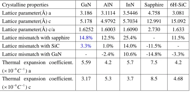
(29) a comparable thermal conductivity of around 1.5 W/cm·K to Si, which is higher than the commonly used compound semiconductor materials. From the superior material properties of GaN, such as high breakdown field, high saturation velocity and wide bandgap, GaN-based electronic devices are indeed good candidates in the high-power, high-temperature and high-speed applications. Table 2-2 lists the structural properties of GaN-based materials, sapphire and SiC substrates. GaN-based materials have the wurtzite crystal structure, which consists of two hexagonal closely packed (HCP) sublattices, group III and nitrogen atoms. The lattice parameters for GaN are 3.186 in a axis and 5.178 Å in c axis. Compared to GaN, the AlN has smaller lattice parameters, while the InN has larger lattice constants. Up to now, the most widely used substrate materials are sapphire and SiC. The reason is that in the early stage there is no suitable substrate material with perfect lattice match to GaN available for the epitaxial growth of GaN-based materials. Currently, although the GaN substrate can be obtained, the available size now is still too small, as compared to the sapphire and SiC substrates. The very large lattice mismatch (14.8%) and the difference in the thermal expansion coefficient between the GaN and sapphire substrate, however, cause huge challenges in the material growth of nitrides. Amano et al. proposed to grow a thin AlN nucleation layer at low temperatures and successfully obtained atomically smooth GaN layers in 1986 [2]. Later, 7.
(30) Nakamura et al. used a GaN nucleation layer grown at low temperatures and obtained the GaN layers with even higher electron mobility [3-4]. On the other hand, the SiC substrates have a much smaller lattice mismatch to GaN and a smaller difference in the thermal expansion coefficients with GaN, so it is much easier to grow GaN-based materials using the SiC substrates. However, the expansive price and the lack of substrates with larger dimensions limit the use of SiC substrates for practical applications. In contrast, the much cheaper price and the availability of substrates with larger sizes enable sapphire substrates to become a very popular substrate material for nitrides.. 2-2 Polarization effect 2-2-1 Crystal structure and polarity Nitride-based materials have the wurtzite crystal structure, which consists of two, group III and nitrogen, interpenetrating hexagonal closely packed (HCP) sublattices, as shown in Fig. 2-1. In general, noncentrosymmetric compound crystals exhibit two different sequences of the atom layering in the two opposing directions parallel to certain crystallographic axes, and thus crystallographic polarity along the axes can be observed. In the epitaxial growth of GaN and GaN-based heterostructures, the most common growth direction is normal to the {0001} basal plane, where the atoms are arranged in bilayers. It is noted that the [0001] direction is given by a vector pointing from a Ga atom to a nearest-neighbor nitrogen atom. As can be seen, if 8.
(31) the gallium atoms are on the top position of the bilayers (left side), it is called the Ga-face structure, corresponding to the [0001] polarity. On the other hand, if the nitrogen atoms are located on the surface of the {0001} bilayers (right side), it is the N-face structure, corresponding to the [000ī] polarity. Crystal structures with different crystallographic polarities exhibit different physical and chemical properties [5]. Usually, the layers grown by metalorganic chemical vapor deposition (MOCVD) are Ga-face structures. The layers grown by molecular beam epitaxity (MBE) are either Ga-face or N-face, depending on the nucleation layer used during material growth [6].. 2-2-2 Spontaneous and piezoelectric polarizations [1, 5, 7] Inside the GaN crystal, the individual atoms are partially ionized, and the large Ga atom and small N atom are arranged somewhat irregularly with respective to each other because of the difference in atomic size. This combination of ionization and irregularity leads to a spontaneous electrical polarization within the GaN crystal. Due to the sensitive dependence of the spontaneous polarization on the structure parameters, the increasing nonideality of the crystal structure going from GaN to AlN further enhances the spontaneous polarization, as shown in Table 2-3. In particular, all the calculated spontaneous coefficients are negative [8]. Here, we consider the polarization along the [0001] direction. Thus the spontaneous polarization along the c-axis of the wurtzite crystal structure is 9.
(32) PSP= PSP z.. (1). In the case of AlGaN/GaN heterostructures, the strain produced at the interface due to the lattice mismatch between the GaN and AlGaN layers gives rise to an electrically charged region by the piezoelectric polarization. From a microscopic point of view, a strain parallel or perpendicular to the c axis produces an internal displacement of the metal sublattice with respective to the nitrogen ones. The measured polarization is due to the effect of the change of the lattice constants and the associated change in the length of the bond parallel to the c axis. The piezoelectric polarization can be calculated as follows. PPE= e33єz + e31(єx + єy),. (2). where e33 and e31 are the piezoelectric coefficients, єz = (c-c0)/c0 is the strain along the c-axis and the in-plane strain, єx = єy = (a-a0)/a0, is assumed to be isotropic. a0 and c0 are lattice parameters. The relation between the lattice constants of the hexagonal AlGaN system is. c − c0 C a − a0 = −2 13 , c0 C33 a0. (3). where C13 and C33 are elastic constants. Using the Eqs (2) and (3), the amount of the piezoelectric polarization in the c-axis direction cab be determined as PPE = 2. a − a0 C (e31 − e33 13 ) . a0 C33. (4). Since the term e31 - e33(C13 /C33) < 0 for AlGaN over the whole Al composition, the piezoelectric polarization is negative for tensile and positive for compressive strained AlGaN layer. 10.
(33) Next, we determine the total polarization at the AlGaN/GaN interface. The spontaneous polarization for GaN and AlN was negative, meaning that for Ga-face heterostructures the spontaneous polarization points towards the substrate. Thus, the alignment in the direction of the piezoelectric polarization and the spontaneous polarization is parallel in the case of the tensile strained AlGaN layer, and is anti-parallel in the case of compressively strained cap AlGaN layer. On the other hand, if the crystal polarity changes from Ga-face to N-face material, the spontaneous and the piezoelectric polarization change the sign, as shown in Fig. 2-2. Furthermore, if the polarization-induced sheet charge is positive, free electrons will tend to compensate the polarization-induced sheet charge. Also, these free electrons will form a two-dimensional electron gas (2DEG) at the AlGaN/GaN interface. In contrast, the negative polarization-induced sheet charge will cause the accumulation of holes at the interface. For Ga(Al)-face AlGaN/GaN heterostructures, the polarization-induced sheet charge is positive in the case of the tensile strained AlGaN [Fig. 2-2 (a)]. Even if the heterostructure is relaxed in case that the AlGaN thickness > 65 nm, the polarization-induced sheet charge is still positive because of the large difference in the spontaneous polarization of GaN and AlN [Fig. 2-2 (b)]. The piezoelectric polarization due to the tensile strain at the interface will further enhances the difference in the total polarization between the AlGaN and GaN, and thus the positive polarization induced sheet charge density and the 2DEG concentration increase accordingly. For N-face AlGaN/GaN heterostructures, the spontaneous and piezoelectric 11.
(34) polarizations have opposite directions to the Ga-face heterostructures. It is therefore that the polarization induced sheet charge is negative and the accumulation of holes forms at the interface [Fig. 2-2 (d) and (e)]. From the above argument, it is therefore obvious that why a 2DEG can be observed by Hall effect measurement and the capacitance–voltage (C-V) profiling technique for the Ga(Al)-face AlGaN/GaN heterostructures. Here, we consider the heterostructures where the AlGaN barriers are grown on the GaN buffer layers and are therefore under tensile strain. In this case, since the spontaneous and piezoelectric polarizations point in the same direction, the value of the total polarization is the sum of the spontaneous and piezoelectric polarizations. P=PPE + PSP,. (5). Associated with the polarization field is a polarization induced charge density given by ρP = -∇⋅P,. (6). At the interface of AlGaN/GaN heterostructures where AlGaN layer is the top layer, the polarization-induced sheet charge density is defined by σ(PSP + PPE) = P (bottom) – P (top) = [PSP (bottom) + PPE (bottom)] - [PSP (top) + PPE (top)] = [PSP (bottom) - PSP (top)] + [PPE (bottom) - PPE (top)] = σ(PSP) + σ(PPE).. (7) 12.
(35) 2-2-3 Strain relaxation [7]. As the AlGaN thickness is increased to a critical value, the critical thickness, we need to consider the strain relaxation effect on the piezoelectric and the total polarization. Calculation of the critical thickness of AlGaN grown on relaxed GaN based on the models proposed by Matthews and Blakeslee (M-B) and Fischer is shown in Fig. 2-3. For a typical barrier thickness of about 300 Å, the strain relaxation and thus the reduction in piezoelectric polarization has to be expected for Al composition of above 0.14 for the M-B model or 0.25 for the Fischer model. The experimental data, however, shows that the strain relaxation was observed for the critical thickness well above the calculated ones over a wide range of alloy composition. The strain relaxation for a 300 Å thick AlGaN barrier was experimentally observed at Al composition of about 0.38. To analyze the reduction of piezoelectric polarization and the total polarization induced sheet charge due to strain relaxation, the degree of relaxation is defined by r ( x) =. a ( x) − a(GaN ) , a0 ( x) − a(GaN ). (8). and the measured degree of relaxation was approximately by ⎧ 0 0 ≤ x < 0.38 ⎪ r ( x) = ⎨3.5 x − 1.33 0.38 ≤ x ≤ 0.67, for d ( AlGaN ) ≈ 30nm . ⎪ 1 0.67 ≤ x < 1 ⎩. (9). Thus, the piezoelectric polarization for partially relaxed AlGaN barriers can be determined 13.
(36) from the measured degree of relaxation by PPE ( x) = 2{r ( x) − 1}{. C ( x) a( x) − a(0) }{e31 ( x) − e33 ( x) 13 } . a( x) C33 ( x). (10). Fig. 2-4 shows the calculated total polarization induced sheet charge under different degrees of relaxation and Al composition. By taking the difference in the spontaneous polarization of GaN and AlGaN into account, the total polarization as well as the corresponding calculated sheet charge decreases with the increasing degree of relaxation.. 2-2-4 Sheet carrier concentration of 2DEG [5, 7]. With a basic understanding of the polarization induced sheet charge, we now wish to predict the sheet charge carrier concentration of a 2DEG and its dependence on the Al composition for strained AlGaN/GaN heterostructures. Free electrons tend to compensate the positive polarization induced sheet charge bound at the lower AlGaN/GaN interface for Ga(Al)-face heterostructures or at the upper GaN/AlGaN interface for N-face heterostructures. For undoped Ga-face AlGaN/GaN heterostructures, the sheet carrier concentration of 2DEG can be calculated by using the total polarization induced sheet charge and the following equation [9]: nS ( x ) =. σ ( x ) ⎛ ε 0ε S ( x ) ⎞ e. ⎟[eφ B ( x) + E F ( x) − ∆EC ( x)] , − ⎜⎜ 2 ⎟ ⎝ d AlGaN e ⎠. (11). where ε(x) is the relative dielectric constant of AlxGa1-xN, dAlGaN is the AlGaN barrier. 14.
(37) thickness, eφB(x) is the Schottky barier of the gate contact on AlGaN, EF(x) is the Fermi level respective to the GaN conduction-band-edge energy and ∆EC(x) is the conduction band offset at the AlGaN/GaN interface. For undoped AlGaN/GaN heterostructures and assuming that the background free carrier concentration can be neglected (< 1016 cm-3), it is found from Eq. (11) that the value of the 2DEG sheet carrier concentration is dominated by the total polarization induced sheet charge, which can be controlled by the alloy composition of the AlGaN barrier. Fig. 2-5 shows a detailed comparison of calculated and measured sheet carrier concentrations of Ga-face AlGaN/GaN heterostructures with AlGaN thickness of about 200 Å and Al composition up to 0.6. As can be seen, a good agreement between the calculated and experimentally determined highest sheet carrier concentration for the undoped and doped heterostructures can be observed. It is thus evident that the measured sheet carrier concentration for undoped structures are higher than the calculated sheet carrier concentration by only the piezoelectric polarization. Therefore, the spontaneous polarization is real and has to be taken into account in the determination of the total polarization sheet charge and 2DEG sheet carrier concentration. Moreover, the predicted sheet carrier concentration induced by the total polarization is more than twice as high as the sheet carrier concentration induced just by the piezoelectric effect.. 2-3 AlGaN/GaN HFETs 15.
(38) 2-3-1 Important issues in the growth of AlGaN/GaN heterostructures. Fig. 2-6 shows the schematic diagram of typical AlGaN/GaN heterostructure field-effect transistors. In general, a thin AlGaN barrier layer with thickness of around 20- 30 nm is pseudomorphically grown on the GaN buffer layer. The GaN buffer layer with both good crystal quality and high resistivity is highly desirable in the fabrication of AlGaN/GaN HFETs. The crystal quality of the GaN buffer layer is crucial to the electron transport properties of the AlGaN/GaN heterostructures. Also, the high-resistivity buffer layer is a necessity for the microwave devices in order to effectively reduce the parasitic capacitances. However, the huge lattice mismatch between the GaN buffer layer and the sapphire substrate causes the formation of very high-density dislocations (~108-109 cm-2) in the epitaxial layers. In order to obtain high-quality GaN buffer layers, the GaN buffer layer is usually very thick, around 2-3 µm. The thicker GaN buffer layer can effectively reduce the defect density and improve the interface roughness of AlGaN/GaN heterostructures, which in turn significantly improves the electron transport properties [10]. In addition, several problems arise in the growth of AlGaN [11]. It is not easy to obtain atomically smooth surfaces, especially for layers with high Al compositions. Also, the local variation in the alloy composition has been observed. As the Al mole fraction is above 0.2, the strain in the AlGaN due to the lattice mismatch between the AlGaN and GaN may cause the formation of structural defects and transition into the island growth mode, and will also 16.
(39) influence the electrical properties of heterostructures.. 2-3-2 Device operation principles. Similar to the configurations of conventional field-effect transistors (FETs), the alloyed Ohmic contacts using Ti/Al-based contact metals act as the source and drain electrodes and the Schottky gates with either Pt/Au or Ni/Au are employed to control the input gate voltage signals. In the operation of FETs, a voltage signal applied to the gate electrode controls the current flow between the source and the drain electrodes. The small voltage changes on the gate are thus amplified into much larger changes in an external circuit. Particularly, the strong spontaneous and piezoelectric polarization that exists naturally in the AlGaN layer leads to the formation of high-density 2DEG at the interface of the undoped AlGaN/GaN heterostructures. It is therefore that the channel doping or the modulation doping, which is neceaasry for conventional heterostructure FETs, becomes unnecessary for the nitride HFETs.. 2-3-3 Device fabrication. Fig. 2-7 shows the process procedures developed for the fabrication of AlGaN/GaN HFETs. The fabrication processes begin with the mesa isolation, followed by the Ohmic contact and the Schottky gate fabrication. Mesa isolation was performed with Cl2/Ar plasma 17.
(40) using an inductively couple plasma (ICP) system. Contact metals including Ti/Al/Ti/Au were then deposited to form the source and drain contact pads. With proper rapid thermal annealing in nitrogen ambient, low resistance Ohmic contacts were obtained. Pt or Ni is used as the Schottky metal because of the larger Schottky barrier height on nitrides. In particular, Ni is the preferred Schottky metal for the submicron T-gate fabrication due to its better adhesion to the underlying nitrides, although the Schottky barrier of Ni is slightly lower than Pt.. 18.
(41) References. [1] L. F. Eastman and U. K. Mishra, IEEE spectrum, May, 28 (2002). [2] H. Amano, N. Sawaki, I. Akasaki and Y. Toyoda, Appl. Phys. Lett., 48, 353 (1986). [3] S. Nakamura, Jpn. J. Appl. Phys., 30, L1705 (1991). [4] S. Nakamura, T. Mukai and M. Senoh, J. Appl. Phys. 71, 5543 (1992). [5] O. Ambacher, J. Smart, J. R. Shealy, N. G. Weimann, K. Chu, M. Murphy, W. J. Schaff, L. F. Eastman, R. Dimitrove, L. Wittmer, M. Stutzmann, W. Rieger and J. Hilsenback, J. Appl. Phys., 85, 3222 (1999). [6] R. Dimitrove, M. Murphy, J. Smart, W. J. Schaff, J. R. Shealy, L. F. Eastman, O. Ambacher and M. Stutzmann, J. Appl. Phys., 87, 3375 (2000). [7] O. Ambacher, B. Foutz, J. Smart, J. R. Shealy, N. G. Weimann, K. Chu, M. Murphy, A. J. Sierakowski, W. J. Schaff, L. F. Eastman, R. Dimitrove, A. Mitchell and M. Stutzmann, J. Appl. Phys., 87, 334 (2000). [8] F. Bernardini, V. Fiorentini and D. Vanderbilt, Phys. Rev. B, 56, R10024 (1997). [9] E. T. Yu, G. J. Sullivan, P. M. Asbeck, C. D. Wang, D. Qiao and S. S. Lau, Appl. Phys. Lett., 71, 2794 (1997). [10] L. F. Eastman, V. Tilak, J. Smart, B. M. Green, E. M. Chumbes, R. Dimitrove, H. Kim, O. Ambacher, N. Weimann, T. Prunty, M. Murphy, W. J. Schaff and J. R. Shealy, IEEE Trans. Electron Devices, 48, 479 (2001). 19.
(42) [11] S. Keller, G. Parish, P. T. Fini, S. Heikman, C. H. Chen, N, Zhang, S. P. DenBaars, U. K. Mishra and Y. F. Wu, J. Appl. Phys., 86, 5850 (1999).. 20.
(43) Table 2-1 Fundamental material properties of several important semiconductors [1].. Table 2-2 Structural properties of GaN-based materials, sapphire and SiC substrates. Crystalline properties. GaN. AlN. InN. Sapphire. 6H-SiC. Lattice parameter(Å) a. 3.186. 3.1114. 3.5446. 4.758. 3.081. Lattice parameter(Å) c. 5.178. 4.9792. 5.7034. 12.991. 15.092. Lattice parameter(Å) c/a. 1.6252. 1.6003. 1.6090. 2.730. 1.633. Lattice mismatch with sapphire. 14.8%. 12.5%. 25.4%. -. 11.5%. Lattice mismatch with SiC. 3.3%. 1.0%. 14.0%. -11.5%. -. Lattice mismatch with GaN. -. -2.4%. 10.6%. -14.8%. -3.3%. 5.59. 4.2. 5.7. 7.5. 4.2. 3.17. 5.3. 3.7. 8.5. 4.68. Thermal expansion coefficient. −6. −1. −6. −1. ( × 10 C ) a Thermal expansion coefficient.. ( × 10 C ) c. 21.
(44) Fig. 2-1 Schematic diagrams of the crystal structure and the polarity of the Ga-face and N-face GaN crystals [5].. Table 2-3 Spontaneous polarization, piezoelectric and dielectric constants of AlN, GaN and InN [5].. 22.
(45) Fig. 2-2 Polarization-induced sheet charge and directions of the spontaneous and piezoelectric polarization in the Ga-face and N-face strained and relaxed AlGaN/GaN heterostructures [5].. 23.
(46) Fig. 2-3 Critical thickness of AlGaN grown on relaxed GaN calculated using the models of Matthews and Blakeslee or Fischer et al. as a function of Al composition. AlGaN layers with different thickness and Al composition grown pseudomorphically on GaN by MOCVD and MBE are marked by black symbols. Partially relaxed AlGaN layers (white symbols) are separated from the pseudomorphic heterostructures by a dash line [7].. 24.
(47) Fig. 2-4 Calculated total polarization induced sheet charge for pseudomorphically grown AlGaN/GaN heterostructures under different degrees of relaxation and Al compositions [7].. Fig. 2-5 Calculated maximum sheet carrier concentration for pseudomorphic (dashed lines) and partially relaxed (solid lines) Ga-face AlGaN/GaN heterostructures with a barrier thickness of 200 Å [7]. 25.
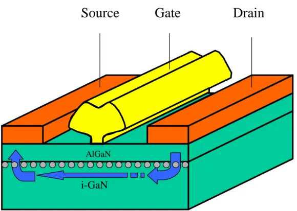
(48) Source. Gate. Drain. AlGaN. i-GaN. Fig. 2-6 The schematic diagram of typical AlGaN/GaN heterostructure field-effect transistor.. 26.
(49) (a) Mesa isolation. AlGaN. i-GaN. (b) Ohmic contacts. AlGaN. i-GaN. (c) Schottky gate. AlGaN. i-GaN. Fig. 2-7 The process procedures for the fabrication of AlGaN/GaN HFETs.. 27.
(50) Chapter 3 Inductively Coupled Plasma Etching of GaN. 3-1 Introduction Nitride-based electronic devices, such as heterostructure field-effect transistors (HFETs) and heterostructure bipolar transistors (HBTs), are potentially very useful for high-power and high-temperature applications. To realize these devices, device isolation is a necessity. Usually device isolation is done by mesa isolation or implantation isolation. Nitride-based materials, due to the inert chemical nature and the strong bonding energies, are not easy to be etched by conventional approaches including the wet chemical etching and the reactive-ion etching (RIE) [1]. In recent years, several new etching techniques such as high-density plasma (HDP) etching, chemically assisted ion beam etching (CAIBE), reactive ion beam etching (RIBE), low electron energy enhanced etching (LE4) and photoassisted dry etching were developed in an attempt to perform etching on the nitride-based materials. Compared with the conventional RIE, the HDP etcher has a much higher plasma density and the capability to more efficiently decouple the ion energy and ion density. Thus, the HDP etching, such as the inductively coupled plasma (ICP) etching, the electron cyclotron resonance (ECR) etching or the magnetron RIE (MRIE), has gradually become a popular approach. In this work, we systematically investigated the inductively coupled plasma etching of GaN. We studied the 28.
(51) dependence of the etching parameters, including the bias power, the Ar flow rate and the Cl2 flow rate, on the etching rate and the etched sidewall profile of GaN. A proper etching rate together with the vertical sidewall profile and smooth surface developed in this work are applicable in the fabrication of GaN-based electronic devices.. 3-2 Experiments The 2-µm-thick undoped GaN films for this study were grown by metalorganic chemical vapor deposition (MOCVD) on c-plane sapphire substrates. After layer growth, mesa patterns for etching tests were defined by photolithography. Ni metal mask of around 2000 Å was then deposited using e-beam evaporation to form the etching mask. The samples were etched by Cl2/Ar plasma using an inductive coupled plasma (ICP) system under different etching conditions. After dry etching, the Ni mask was removed using the solution HNO3: H2O= 1:1. After etching, the etching depth, sidewall profile and the surface morphology were characterized.. 3-3 Results and Discussion 3-3-1 Ni mask fabrication Usually, aggressive etching conditions were required in the dry etching of nitrides because of the inert chemical nature and strong bonding energies. Photoresist, Ni metal mask 29.
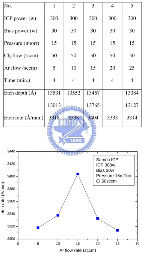
(52) and SiO2 oxide mask can be used as the masking materials. In this work, we choose Ni metal as the etching mask due to its excellent masking ability. Wet etching and lift-off process were employed to fabricate Ni masks. The mesa patterns in Ni formed by a lift-off process were shown to be much better than those by the wet etching process. Fig. 3-1 shows the Ni patterns after lift-off. Smooth edges and sharp profiles were obtained. In contrast, if the mesa patterns are defined by the wet chemical etching, rough edges will result, as shown in Fig. 3-2.. 3-3-2 ICP etching A couple of etching conditions were used to investigate the ICP etching of GaN, as summarized in Tables 3-1 to 3-3. The chemical species used here is Cl2. Ar is used to assist the etching process. Table 3-1 is for etching under different Ar flow rates, Table3-2 is for etching under different bias powers and Table 3-3 is for etching under different Cl2 flow rates. Figure 3-3 shows the etching rates as a function of the Ar flow rate. The ICP power, the bias power, the chamber pressure and the Cl2 flow rate used here were 300 W, 30 W, 15 mtorr and 50 sccm, respectively. The Ar flow rate ranged from 5 to 25 sccm. Etching rates of around 3300 Å/min. to 3400 Å/min. were obtained. A slight increase in the etching rate was observed in the cases where the Ar flow rate was increased from 5 to 15 sccm. With a higher Ar flow rate of above 15 sccm, the etching rate decreases. Fig. 3-4 shows the SEM images of the 30.
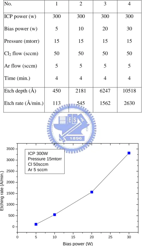
(53) sidewall profile and the surface morphology after etching. As a whole, the surface morphology of the etched surface is very smooth for all etching conditions used. For the samples treated with the Ar flow rate of 5 to 20 sccm, vertical sidewall profiles were obtained. The sample etched with an Ar flow rate of 25 sccm showed a slight undercut sidewall profile. Part of the samples showed slightly rough edge, such as Fig. 3-2 (b) and (d), which was attributed to the poor Ni mask edge profile. In general, a higher Ar flow rate can enhance the physical ion bombardment, leading to more efficient bond breaking and the desorption of etched products. Thus the increase in the Ar flow rate can enhance the etching rate. As can be seen, a slight increase in the etching rate was obtained for samples with Ar flow rate below 15 sccm. On the other hand, a higher Ar flow rate may cause the decrease in the Cl2/Ar flow rate ratio, leading to the decrease in the etching rate. In addition, a higher Ar flow rate can enhance the vertical etching, resulting in vertical sidewall profiles. The sidewall profiles obtained are vertical for most samples except the sample with Ar flow rate of 25 sccm. Figure 3-5 shows the etching rate as a function of the bias power. An ICP power of 300 W, a chamber pressure of 15 mtorr, a Cl2 flow rate of 50 sccm and a Ar flow rate of 5 sccm were used. The etching rate increased with the bias power. When the bias power was reduced to 5 W, a very slow etching rate of around 100 Å/min was obtained. Figure 3-6 shows the SEM images of the etched sidewall profile. As a whole, vertical sidewall profile and smooth 31.
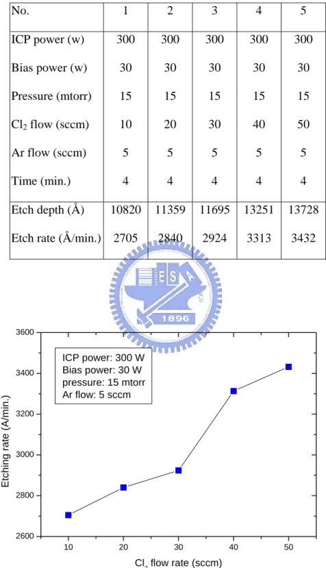
(54) etched surface were obtained for most samples. The sample treated with a bias power of 20 W showed a slight undercut sidewall. The rough edge obtained in Fig. 3-4 (b) is due to the rough edge of the Ni metal mask. The rough etched surface shown in Fig. 3-4 (d) is mainly attributed to the poor surface treatment before dry etching. Similar to the cases in Ar flow rate, the increase in the bias power can increase the kinetic energies of the incident ions and thus enhance physical ion bombardments. Therefore, higher etching rate can be obtained. The increase in the bias power can also enhance the vertical sidewall profile as a result of the stronger physical ion bombardments. Figure 3-7 shows the etching rate under different Cl2 flow rates. The Cl2 flow rate ranged from 10 to 50 sccm. The other dry etching parameters such as the ICP power, the bias power, the chamber pressure and the Ar flow rate were fixed, as shown in Table 3-3. The etching rate increased with the Cl2 flow rate. This is because more reactive Cl radicals were generated to participate in the surface chemical reaction as a higher Cl2 flow rate was employed. Fig. 3-8 shows the SEM images of the sidewall profile and the surface morphology. Very sharp sidewall profile and very smooth surface were observed in all samples, indicating that the change in the Cl2 flow rate does not have a significant influence on the etched sidewall profile and surface morphology.. 3-4 Conclusions 32.
(55) We systematically investigated the ICP etching of GaN. We studied the process for the Ni mask fabrication. Ni masks fabricated by the lift-off process have very smooth edge and excellent dimension control. In addition, the dependence of the etching rate and the etched sidewall profile of GaN on the etching parameters, such as the bias power, the Ar flow rate and the Cl2 flow rate, were studied. A larger bias power can enhance the etching rate and the vertical sidewall profiles as a result of the stronger physical ion bombardments. Proper adjustment in the Ar flow rate also enhances the etching rate and the vertical sidewall profiles. The increase in the Cl2 flow rate increases the etching rate since more reactive Cl radicals are generated to react with the underlying GaN. But no obvious change in the etched sidewall profiles was observed. A proper etching rate together with the vertical sidewall profile and smooth surface developed in this work are applicable in the fabrication of GaN-based devices.. 33.
(56) References [1] S. J. Pearton, J. C. Zolper, R. J. Shul and F. Ren, J. Appl. Phys. 86, 1 (1999).. 34.
(57) Fig. 3-1 Optical microscope (OM) images of the Ni metal masks. This is done after lift-off process was performed.. Fig. 3-2 Optical microscope (OM) images of the Ni metal mask, where the black parts represent the etched Ni mask and the outer transparent parts represent photoresists. This is done by the wet etching process.. 35.
(58) Table 3-1 Etching condition where the Ar flow rate was modulated. No.. 1. 2. 3. 4. 5. ICP power (w). 300. 300. 300. 300. 300. Bias power (w). 30. 30. 30. 30. 30. Pressure (mtorr). 15. 15. 15. 15. 15. Cl2 flow (sccm). 50. 50. 50. 50. 50. Ar flow (sccm). 5. 10. 15. 20. 25. Time (min.). 4. 4. 4. 4. 4. 13531. 13552. 13467. 13384. 13765. 13127. Etch depth (Å). 13013 Etch rate (Å/min.) 3318. 3338. 3404. 3333. 3314. 3440. Samco ICP ICP 300w Bias 30w Pressure 15mTorr Cl 50sccm. 3420. etch rate (A/min). 3400. 3380. 3360. 3340. 3320. 3300 0. 5. 10. 15. 20. Ar flow rate (sccm). Fig. 3-3 Etching rates under different Ar flow rates.. 36. 25. 30.
(59) (a) Ar flow: 5 sccm. (b) Ar flow: 10 sccm. (c) Ar flow: 15 sccm. (d) Ar flow: 20 sccm. (e) Ar flow: 25 sccm Fig. 3-4 SEM images of the sidewall profile after ICP etching was performed under different Ar flow rates.. 37.
(60) Table 3-2 Etching condition where the bias power was modulated. No.. 1. 2. 3. 4. ICP power (w). 300. 300. 300. 300. Bias power (w). 5. 10. 20. 30. Pressure (mtorr). 15. 15. 15. 15. Cl2 flow (sccm). 50. 50. 50. 50. Ar flow (sccm). 5. 5. 5. 5. Time (min.). 4. 4. 4. 4. Etch depth (Å). 450. 2181. 6247. 10518. Etch rate (Å/min.). 113. 545. 1562. 2630. 3500. ICP 300W Pressure 15mtorr Cl 50sccm Ar 5 sccm. Etching rate (A/min.). 3000 2500 2000 1500 1000 500 0 0. 5. 10. 15. 20. Bias power (W). Fig. 3-5 Etching rate under different bias powers.. 38. 25. 30.
(61) (a) Bias power: 5 w. (b) Bias power: 10 w. (c) Bias power: 20 w. (d) Bias power: 30 w. Fig. 3-6 SEM images of the sidewall profile after ICP etching was performed under different bias power.. 39.
(62) Table 3-3 Etching condition where the Cl2 flow was modulated. No.. 1. 2. 3. 4. 5. ICP power (w). 300. 300. 300. 300. 300. Bias power (w). 30. 30. 30. 30. 30. Pressure (mtorr). 15. 15. 15. 15. 15. Cl2 flow (sccm). 10. 20. 30. 40. 50. Ar flow (sccm). 5. 5. 5. 5. 5. Time (min.). 4. 4. 4. 4. 4. 10820. 11359. 11695. 13251. 13728. Etch rate (Å/min.) 2705. 2840. 2924. 3313. 3432. Etch depth (Å). 3600. Etching rate (A/min.). 3400. ICP power: 300 W Bias power: 30 W pressure: 15 mtorr Ar flow: 5 sccm. 3200. 3000. 2800. 2600 10. 20. 30. Cl2 flow rate (sccm). Fig. 3-7 Etching rate as a function of the Cl2 flow rate.. 40. 40. 50.
(63) (a) Cl2 flow rate: 10 sccm. (b) Cl2 flow rate: 20 sccm. (c) Cl2 flow rate: 30 sccm Fig. 3-8 SEM images of the sidewall profile after ICP etching was performed under different Cl2 flow rates.. 41.
(64) (d) Cl2 flow rate: 40 sccm. (e) Cl2 flow rate: 50 sccm Fig. 3-8 SEM images of the sidewall profile after ICP etching was performed under different Cl2 flow rates.. 42.
(65) Chapter 4 Low resistance Ohmic contacts to n-GaN. 4-1 Introduction Nitride-based electronic devices, such as heterostructure field-effect transistors (HFETs) and heterostructure bipolar transistors (HBTs), are potentially very useful for high-power and high-temperature applications due to their excellent material properties. To use these devices for such applications, good Ohmic contacts with low contact resistance and good thermal stability are very important. In general, Ohmic contacts to n-GaN with low contact resistance are not easily obtainable because of its wide bandgap. The contact resistance could be improved by various approaches, such as the selection of right contact metal [1-7], the surface treatments [8-9] and the plasma treatments [10-16]. In particular, proper surface plasma treatment has been shown to be very effective in the improvement of contact resistance. Several studies on the thermal stability of Ohmic contacts to GaN have been performed [17-20], however, the thermal stability of the plasma-treated Ohmic contacts has not been studied. Whether the damages created or the defects generated by plasma treatment have any effect on the reliability of the device contacts needs to be answered. In addition, thermal annealing is also very important. Thermal annealing in N2 gas ambient was usually employed to obtain low resistance Ohmic contacts. The main reason for using nitrogen gas as the 43.
(66) annealing ambient instead of hydrogen containing gas, as commonly used by most III-V compounds, is to avoid the effect of hydrogen passivation of dopants in GaN [5]. In this work, we carried out extensive investigations on the Ohmic contacts to n-GaN. Various plasma treatments using Cl2/Ar or Ar species were employed to improve the contact resistance of n-GaN. Additionally, thermal aging tests were performed to further observe the thermal stability of the plasma-treated Ohmic contacts. Moreover, we compared the contact resistance of the samples annealed in forming gas ambient with those in N2 ambient so as to observe if forming gas ambient is applicable to the thermal annealing process of n-GaN. We found that proper plasma treatment can significantly improve the contact resistance. No obvious degradation of contact resistance was observed after aging at 600°C for 2 h in N2 and air ambient. Furthermore, the forming gas was shown to further improve the contact resistance of n-GaN.. 4-2 Experiments The 2-µm-thick n-GaN films for this study were grown by metalorganic chemical vapor deposition (MOCVD) on c-plane sapphire substrates. Samples with different doping concentrations, 8.7×1016 cm-3 and 3.3×1018 cm-3, were used. After layer growth, mesa patterns for transmission line measurement (TLM) were defined by photolithography. Prior to contact metal deposition, the samples were treated by Cl2/Ar or Ar plasma using an inductive coupled 44.
(67) plasma (ICP) system and then dipped in the solution of 1:1 HCl:H2O for 1 min. Contact metal, Ti/Al/Ti/Au (200/1500/450/550 Å), was deposited and lifted-off to form the contact pads. The dimension of contact pad was 100×100 µm2. The samples were annealed at 750°C for 30 s in N2 ambient or forming gas ambient. Aging tests were carried out at temperatures ranging from 400 to 600°C for 2 h in N2 or air ambient to observe the thermal stability of plasma-treated Ohmic contacts. The TLM measurement was then performed for the determination of the contact resistance.. 4-3 Results and Discussion 4-3-1 Plasma treatments Various treatments using Cl2/Ar or Ar plasma were employed to improve the contact resistance of n-type GaN. Samples with different doping concentrations, 8.7×10¹⁶ and 3.3×1018 cm-3, were used to observe the strength of plasma treatments.. Part 1. n-GaN with ND=8.7×1016 cm-3 The conditions of the plasma treatment and the TLM results are shown in Table 4-1. It should be noted that a very low bias power of 5 W was used in the plasma treatment to ensure a very slow etching rate for GaN. For the conditions used here, only about 100-200 Å was etched during the plasma treatment. After annealing at 750°C for 30 s in a N2 ambient, all 45.
(68) samples showed Ohmic behavior. For Cl2/Ar plasma treated samples, the contact resistances were 0.638, 0.614, and 0.28 Ω⋅mm for treatment times of 0, 1 and 2 min. (sample Nos. 1, 2, and 6), respectively. As expected, samples with a longer treatment time have better contact resistances. We also found that Ar flow rate has a significant influence on the contact resistance. Sample No. 5, which was treated with a flow rate ratio of Cl2/Ar = 50/20 for 2 min., has the best result. Its contact resistance and specific contact resistance are 0.21 Ω⋅mm and 6.8x10⁻⁷ Ω⋅cm2, respectively. For samples treated with Ar plasma only, the contact resistance and specific contact resistance decrease with the Ar flow rate. The best results are obtained for an Ar flow of 50 sccm. The contact resistance and specific contact resistance are 0.3 Ω⋅mm and 8.7x10⁻⁷ Ω⋅cm2, respectively.. Part 2. n-GaN with ND=3.3×1018 cm-3 The conditions of the plasma treatment are shown in Table 4-2. Figure 4-1 shows the current-voltage characteristics of the as-deposited Ohmic contacts under different Ar flow rates. With the increase of Ar flow, the current-voltage characteristics of these contacts became more linear. Fig. 4-2 shows the dependence of the contact resistance and the specific contact resistance on the Ar flow rate. Both the contact resistance and specific contact resistance decreased as the Ar flow rate was increased. For samples without Ar plasma treatment, the contact resistance and the specific contact resistance were too high to be 46.
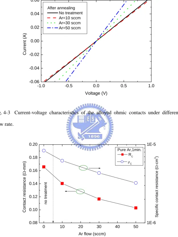
(69) extracted via the TLM measurement. Samples treated with an Ar flow rate of 50 sccm showed the best result. Their contact resistance and specific contact resistance were 0.362 Ω⋅mm and 3.9×10⁻⁵ Ω⋅cm2, respectively. After annealing, all samples showed linear current-voltage characteristics, as shown in Fig. 4-3. Similar dependences of the contact resistance and the specific contact resistance of the alloyed contacts on Ar flow rate were obtained as well, as shown in Fig. 4-4. All alloyed contacts have low contact resistances. Samples treated with 50 sccm of Ar flow rate still exhibited the best electrical characteristics. Their contact resistance and specific contact resistance were 0.103 Ω⋅mm and 3.2×10⁻⁶ Ω⋅cm2, respectively. Apparently, the Ar flow rate has a significant influence on contact resistance. With the increase of Ar flow rate, the contact resistance is improved markedly. The mechanism of Ar plasma etching is physical ion bombardment. Higher Ar flow rate generates higher Ar ion density in the plasma, which enhances the effect of ion bombardment on wafer surface. Thus more lattice damage and crystalline defects are created on wafer surface. The increase of the nitrogen vacancies on wafer surface after plasma treatment has been shown by many researchers [10, 13, 15] and they are generally believed to be native donors [21-22]. Therefore, after plasma treatment with Ar, the improvement of contact resistance is attributed to the increase of nitrogen vacancies on the wafer surface. Figure 4-5 shows the current-voltage characteristics of the as-deposited Ohmic contacts (before annealing) with different Ar treatment times. We found that Ar treatment improves the 47.
(70) Ohmic contact if the duration is less than 1 minute. But if it is too long, the Ohmic contact becomes worse. After a 3 min. of Ar plasma treatment, the current-voltage characteristics are even poorer than those without treatment. After thermal annealing, all samples show good Ohmic behavior, as shown in Fig. 4-6. Substantial improvement can be obtained for the samples treated with shorter times (t = 1, 2 min.). Figure 4-7 shows the dependence of contact resistance and specific contact resistance of the alloyed contacts on the treatment time. As a whole, samples with different treatment times all have lower contact resistances and specific contact resistances than those without treatment. However, for the best result, the treatment time has to be kept no longer than 1 min. The sample with 1 min. of Ar plasma treatment has the lowest contact resistance (0.103 Ω⋅mm) and specific contact resistance (3.2×10⁻⁶ Ω⋅cm2). Plasma treatment not only produces nitrogen vacancies on the surface, which is desirable for the improvement of contact resistance, but also causes crystalline defects, which can degrade the film quality and the contact resistance [12]. So to use such technique for contact improvement, one has to carefully choose the treatment time so that the damage it causes does not overwhelm the benefit it produces.. 4-3-2 Thermal stability issue Samples with an electron concentration of 8.7×1016 cm-3 and treated with Cl2/Ar or Ar plasma were used to study the thermal stability of the plasma-treated Ohmic contacts to 48.
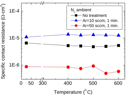
(71) n-GaN. Figures 4-8 to 4-10 show the contact resistance and the specific contact resistance versus aging temperature ranging from 400 to 600°C in N2 ambient. Figures 4-8 and 4-9 are for the Cl2/Ar treated samples and Fig. 4-10 is for the Ar treated samples. As a whole, there is no obvious electrical degradation after aging at 600°C for 2 h for samples either with or without the plasma treatment. The above results indicate that the TiN layer formed at the interface after thermal annealing is thermodynamically stable under this aging condition. Another notable issue is the thermal stability of plasma damage caused by plasma treatment. It is generally believed that the improvement of contact resistance after plasma treatment is mainly due to the formation of nitrogen vacancies on the wafer surface. High-temperature annealing would improve the crystal quality of the GaN epilayer and reduce the defect density on the wafer surface [23]. Although the effect of high-temperature aging on the recovery of the plasma-induced damages is largely unknown, the results obtained here indicate that this annealing effect does not lead to electrical degradation of plasma-treated Ohmic contacts. For samples that were aged in air ambient, similar results were obtained, as shown in Fig. 4-11. The plasma-treated Ohmic contacts were also measured at high temperatures. At 300°C, sample No. 5 still maintains a very low contact resistance (0.412 Ω⋅mm) and a low specific contact resistance (9.3x10⁻⁷ Ω⋅cm2), which are lower than those measured at room temperature of samples without plasma treatment (sample No. 1). Thus, from the thermal. 49.
(72) aging tests and their high-temperature characteristics, it is apparent that the plasma-treated Ohmic contacts exhibited excellent thermal stability.. 4-3-3 Forming gas ambient treatments Samples with an electron concentration of 3.3×1018 cm-3 and treated with Cl2/Ar or Ar plasma were used to study the influence of the forming gas ambient treatment on the plasma-treated Ohmic contacts to n-GaN. Figure 5-8 shows the current-voltage characteristics of the Ohmic contacts after annealing in forming gas (15% H2). All samples showed good Ohmic behavior. In comparison with the samples without plasma treatment, substantial improvement in electrical characteristics was obtained as well. Fig. 5-9 shows the comparison of specific contact resistance of the Ohmic contacts annealed in N2 and in forming gas ambient. Similar to the results of those annealed in N2 gas, the specific contact resistance of the samples annealed in forming gas decreases with the Ar flow rate. It is apparent that the forming gas treated contacts have lower specific contact resistance than those annealed in N2 gas ambient. The lowest contact resistance and specific contact resistance obtained here are 0.093 Ω⋅mm and 2.6×10⁻⁶ Ω⋅cm2, respectively. Obviously, from the results presented above, annealing in forming gas is better than annealing in N2. The possible reason is the reduction capability of the forming gas because of the H2 content. It may reduce the oxidation reaction of metal at high temperatures and 50.
(73) therefore help reduce the contact resistance. Similar results were also observed in the Al/n-GaN Ohmic contacts annealed in Ar/4% H2 forming gas [24]. The H2 content, however, may cause concerns in carrier concentration reduction because of hydrogen passivation. It is known that hydrogen passivation of p-type dopants in p-GaN would result in a large decrease of hole concentration [25-26]. Whether annealing in forming gas ambient would lead to similar reduction in electron concentration and increase in the contact resistance of n-GaN needs to be answered. During annealing process, H2 could diffuse into the bulk n-GaN to form neutral complexes with dopants at annealing temperature higher than 500°C. On the other hand, high temperature annealing process would also result in the dissociation of neutral dopant-H complexes [27]. Although the effect of hydrogen passivation of n-type dopants in n-GaN during the annealing and subsequent cooling process is not completely known, the results obtained here indicate that annealing in forming gas ambient would not lead to electrical degradation of Ohmic contacts.. 4-4 Conclusions We extensively investigated the Ohmic contacts to n-GaN. Proper treatments using the Cl2/Ar or Ar plasma can effectively improve the contact resistance for n-GaN with a doping concentration ranging from 8.7×1016 cm-3 to 3.3×1018 cm-3. Particularly, the Ar flow rate can have a significant effect on contact resistance. We also studied the high temperature thermal 51.
(74) stability of plasma-treated Ohmic contacts to n-GaN. Although the thermal treatment may have some annealing effect on the plasma-generated defects, which are known to be the reason for low contact resistance. No obvious degradation in contact resistance was observed after aging for 2 h in either N2 or air ambient. Thus the thermal stability of plasma-treated Ohmic contacts is not affected by the recovery of plasma-induced damages on the wafer surface. Furthermore, we studied the influence of the forming gas ambient treatments. Even lower contact resistance and specific contact resistance were obtained for contacts annealed in forming gas ambient than those annealed in N2 ambient. This indicates that the electrical characteristics of Ohmic contacts would not influenced by the effect of hydrogen passivation of dopants in n-GaN. We experimentally demonstrated that the plasma-treated Ohmic contacts to n-GaN, with low contact resistance and excellent thermal stability, are highly applicable for the nitride-based electronic devices in high-power and high-temperature applications.. 52.
數據
![Table 2-3 Spontaneous polarization, piezoelectric and dielectric constants of AlN, GaN and InN [5]](https://thumb-ap.123doks.com/thumbv2/9libinfo/8562324.188521/44.892.208.688.789.1115/table-spontaneous-polarization-piezoelectric-dielectric-constants-aln-gan.webp)
+7

相關文件
Al atoms are larger than N atoms because as you trace the path between N and Al on the periodic table, you move down a column (atomic size increases) and then to the left across
substance) is matter that has distinct properties and a composition that does not vary from sample
Students are asked to collect information (including materials from books, pamphlet from Environmental Protection Department...etc.) of the possible effects of pollution on our
Wang, Solving pseudomonotone variational inequalities and pseudocon- vex optimization problems using the projection neural network, IEEE Transactions on Neural Networks 17
The accuracy of a linear relationship is also explored, and the results in this article examine the effect of test characteristics (e.g., item locations and discrimination) and
Then, we tested the influence of θ for the rate of convergence of Algorithm 4.1, by using this algorithm with α = 15 and four different θ to solve a test ex- ample generated as
Particularly, combining the numerical results of the two papers, we may obtain such a conclusion that the merit function method based on ϕ p has a better a global convergence and
Consistent with the negative price of systematic volatility risk found by the option pricing studies, we see lower average raw returns, CAPM alphas, and FF-3 alphas with higher
