應用數位錯誤截取之混合式
三角積分調變器
研究生:楊文霖
指導教授:洪崇智 博士
應用數位錯誤截取之混合式三角積分調變器
Hybrid Sigma-Delta Modulator with Digital Error Truncation
研 究 生:楊文霖 Student:Wen-Lin Yang
指導教授:洪崇智 博士 Advisor:Dr. Chung-Chih Hung
國 立 交 通 大 學
電 信 工 程 學 系 碩 士 班
碩 士 論 文
A Thesis
Submitted to Department of Communication Engineering College of Electrical and Computer Engineering
National Chiao Tung University In Partial Fulfillment of the Requirements
for the Degree of Master in
Communication Engineering September 2008 Hsinchu, Taiwan.
應用數位錯誤截取之混合式三角積分調變器
研究生:楊文霖 指導教授:洪崇智 教授
國立交通大學
電信工程學系碩士班
摘要
三角積分類比數位轉換器傳統地被使用在低訊號頻帶和高解析度的儀器、聲 音和音頻訊號的應用上。在最近幾年,已經有著成長趨勢在發展類比數位轉換器 向系統的前端。由於超大型積體電路技術在尺寸上的縮減,高效能的數位系統能 被實現。類比數位轉換器必須在類比和數位資料的介面提供更高的動態範圍。因 此,能完成用在寬輸入頻帶的無線和有線通訊系統上的高解析度三角積分類比數 位轉換器變成愈來愈重要。 在這論文裡,連續時間調變器的設計流程將被呈現,並且一個應用於藍芽技 術之 100MHz 取樣頻率和 1MHz 訊號頻帶的運算放大器連續時間三角積分類比數位 轉換器被實現。此設計被製造於台積電 0.18 微米互補式金氧半導體製程。量測 的訊號失真雜訊比為 56.8dB 而動態輸入範圍為 60dB。功率消耗在 1.8V 電源供 給下為 22.2 毫瓦。 另一個三角積分設計是去結合連續和離散時間調變器的優點。它是應用數位 錯誤截取之混合式三角積分調變器。此設計製造於台積電 0.13 微米互補式金氧 半導體製程。模擬結果在 62.5MHz 取樣頻率和 2MHz 訊號頻帶下,訊號失真雜訊 比為 60.6dB。這樣規格的調變器可以應用在無線通訊系統 WCDMA 上。功率消耗 在 1.2V 電源供給下為 12.17 毫瓦。Hybrid Sigma-Delta Modulator with Digital Error Truncation
Student:Wen-Lin Yang Advisor:Prof. Chung-Chih Hung
Department of Communication Engineering National Chiao Tung University
Hsinchu, Taiwan
Abstract
Sigma-delta analog-to-digital converters (ADCs) are traditionally used in instrumentation, voice, and audio applications that require low signal bandwidth and high resolution. In recent years, there has been a growing trend to move ADC towards the system front-end. Due to the scaling in VLSI technology, high performance digital systems can be realized. The ADC has to provide a higher dynamic range for the interface between analog and digital data. Therefore, sigma-delta ADCs which can achieve high resolution with wide input bandwidth for wireless and wireline communication systems becomes more and more important.
In this thesis, the design flow of the continuous-time (CT) modulator is presented and a 100MHz CT single-bit active-RC sigma-delta modulator with 1MHz signal bandwidth for Bluetooth application is implemented. The design has been fabricated by TSMC 0.18μm CMOS process. The measured SNDR is 56.8dB and the dynamic range is about 60dB. The power consumption is about 22.2mW at 1.8V supply.
The other sigma-delta design is to combine the advantages of the CT and discrete-time (DT) modulators. It is a hybrid sigma-delta modulator with digital error truncation. The work is designed in TSMC 0.13μm CMOS process. The simulation result shows 60.6dB SNDR for 62.5MHz sampling frequency and 2MHz signal bandwidth. With such specification, the modulator can be applied to WCDMA wireless communication system. The power consumption is about 12.17mW at 1.2V supply.
誌謝
隨著這份碩士論文的完成,兩年來在交大的求學生活也即將告一個段落,往 後迎接著我的,又是另一段嶄新的人生旅程。本論文得以順利完成,首先,要感 謝我的指導教授洪崇智老師在我兩年的研究生活中,對我的指導與照顧,並且在 研究主題上給予我寬廣的發展空間。而類比積體電路實驗室所提供完備的軟硬體 資源,讓我在短短兩年碩士班研究中,學習到如何開始設計類比積體電路,乃至 於量測電路,甚至單獨面對及思考問題的所在。此外要感謝李育民教授和溫宏斌 教授撥冗擔任我的口試委員並提供寶貴意見,使得本論文更為完整。也感謝國家 晶片系統設計中心提供先進的半導體製程,讓我有機會將所設計的電路加以實現 並完成驗證。 另一方面,要感謝所有類比積體電路實驗室的成員兩年來的互相照顧與扶 持。首先,感謝已畢業博士班學長羅天佑和博士班學長薛文弘、黃哲揚以及已畢 業的碩士班學長林明澤、吳國璽、邱建豪、高正昇、廖德文和白逸維在研究上所 給予我的幫助與鼓勵,尤其是文弘學長,由於他平時不吝惜的賜教與量測晶片時 給予的幫助,使得我的論文研究得以順利完成。另外我要感謝林永洲、郭智龍、 夏竹緯、邱楓翔、黃介仁和張維欣等諸位同窗,透過平日與你們的切磋討論,使 我不論在課業上,或研究上都得到了不少收穫。尤其是工四718實驗室的同學們, 兩年來陪我ㄧ塊兒努力奮鬥,一起渡過同甘苦的日子,也因為你們,讓我的碩士 班生活更加多采多姿,增添許多快樂與充實的回憶。此外也感謝學弟們李尚勳、 黃聖文、許新傑、簡兆良的熱情支持,因為你們的加入,讓實驗室注入一股新的 活力與朝氣。 到這邊,特別要致上最深的感謝給我的父母及家人們,謝謝你們從小到大所 給予我的栽培、照顧與鼓勵,讓我得以無後顧之憂地完成學業,朝自己的理想邁 進,衷心感謝你們對我的付出。還有默默陪伴著我的女友淑宜,感謝妳體諒我平 時的忙碌,以及在背後不斷地鼓勵我、支持我,並在這段成長的路上與我相伴。 最後,所有關心我、愛護我和曾經幫助過我的人,願我在未來的人生能有一 絲的榮耀歸予你們,謝謝你們。楊文霖 于 交通大學工程四館 718 實驗室 2008.8.20
Page ABSTRACT………...I ACKNOWLEGEMENT………...III TABLE OF CONTENTS………...IV LIST OF FIGURES………..VII LIST OF TABLES………...X Page CHAPTER 1 Introduction ...1 1.1 Motivation...1 1.2 Thesis Organization ...2
CHAPTER 2 Basic Understanding of Sigma-Delta A/D Conversion...4
2.1 Performance Parameters ...4
2.1.1 Signal-to-Noise Ratio (SNR) ...4
2.1.2 Signal-to-Noise and Distortion Ratio (SNDR) ...5
2.1.3 Spurious Free Dynamic Range (SFDR)...5
2.1.4 Dynamic Range (DR) ...5
2.1.5 Effective Number of Bits (ENOB) ...5
2.1.6 Overload Level (OL)...6
2.2 Sampling and Quantization...6
2.3 White Noise ...10
2.4 Oversampling...12
2.5 Noise shaping strategy ...13
2.5.1 First-Order Sigma-Delta Modulator ...14
2.5.2 Second-Order Sigma-Delta Modulator ...16
2.5.3 Higher-Order Sigma-Delta Modulators ...18
2.5.4 Multi-Stage Modulators ...19
2.6 Summary...20
CHAPTER 3 Continuous-Time Sigma-Delta Modulators...21
3.1 Discrete-Time / Continuous-Time Modulators...21
3.2 Transformation of a Discrete-Time to a Continuous-Time...22
3.3 Non-idealities of Continuous-Time Modulators ...27
3.3.2 Excess Loop Delay ...28
3.3.3 Clock Jitter ...30
CHAPTER 4 A Continuous-Time Single-Bit Active-RC Sigma-Delta Modulator for Bluetooth...33
4.1 Introduction...33
4.2 Loop Filter Architecture...33
4.2.1 Architecture...33
4.2.2 Coefficients ...35
4.3 System Level Analysis...36
4.3.1 RC Variation...38
4.3.2 Excess Loop Delay ...38
4.3.3 Clock Jitter ...39
4.3.4 Simulation Result...40
4.4 Circuit Level Implementation ...41
4.4.1 Operation Amplifier of the First Stage...41
4.4.2 Operation Amplifier of the Second & Third Stage ...44
4.4.3 Comparator ...45
4.4.4 Current Steering DAC...47
4.4.5 Clock Generator ...48
4.4.6 Tuning Circuit ...48
4.4.7 Simulation Result...49
4.5 Layout Design...50
4.6 Summary...52
CHAPTER 5 Hybrid Sigma-Delta Modulator with Digital Error Truncation ....53
5.1 Introduction...53
5.2 Truncation error shaping and cancellation...54
5.2.1 Truncation Error Shaping...54
5.2.2 Truncation Error Cancellation ...56
5.3 Switched-Capacitor Resistor (SCR) Feedback DAC...58
5.4 Hybrid Sigma-Delta Modulator with Digital Error Truncation ...60
5.4.1 System Level Analysis...61
5.4.1.1 The Word-length of Digital Sigma-Delta Modulator...61
5.4.1.2 Non-idealities of Integrators ...62
5.4.1.3 RC Variation...63
5.4.1.4 Clock Jitter ...63
5.4.1.5 Simulation Result...64
5.4.2 Circuit Level Implementation ...65
5.4.2.2 Operation Amplifier of the Second Stage ...69 5.4.2.3 17-level Quantizer...71 5.4.2.4 Clock Generator ...72 5.4.2.5 Tuning Circuit ...74 5.4.2.6 Encoder ...75 5.4.2.7 Adder & DFF ...75 5.4.2.8 Simulation Result...77 5.4.3 Layout Design...79 5.5 Summary...80
CHAPTER 6 Test Setup and Measurement Results...81
6.1 Introduction...81
6.2 Measuring Environment...81
6.2.1 Power Supply Regulator ...83
6.2.2 Single-to-Differential Transformer ...84
6.2.3 Reference Voltage Generator ...85
6.3 PCB and Pin Configurations...85
6.4 Measurement Results ...88
6.4.1 A Continuous-Time Single-Bit Active-RC Sigma-Delta Modulator for Bluetooth ...88
6.4.2 Hybrid Sigma-Delta Modulator with Digital Error Truncation ...90
6.5 Summary...90
CHAPTER 7 Conclusions and Future Works...92
7.1 Conclusions...92
7.2 Future Works...93
Figure Page
2.1 Performance of the SFDR...5
2.2 Performance characteristic of a sigma-delta modulator...6
2.3 Spectral of the sampling operation ...7
2.4 Aliasing phenomenon...7
2.5 M-step mid-rise quantizer (M is odd) (a) transfer curve (b) error function...8
2.6 M-step mid-tread quantizer (M is even) (a) transfer curve (b) error function ...9
2.7 Basic A/D structure ...9
2.8 A quantizer and its linear quantizer model...10
2.9 (a) Probability density function (b) Power spectral density of quantization noise 11 2.10 Power spectral density (a) without oversampling (b) with oversampling ...12
2.11 (a) A general sigma-delta modulator (b) Its linear model in z domain ...14
2.12 A first-order lowpass sigma-delta modulator...15
2.13 A second-order lowpass sigma-delta modulator ...17
2.14 Comparison with different noise shaping transfer functions ...17
2.15 A higher-order lowpass sigma-delta modulator ...18
2.16 A second-order MASH modulator ...20
3.1 (a) A first order CTSDM (b) A first order DT SDM ...21
3.2 (a) CT (b) DT sigma-delta modulator ...23
3.3 Open-loop (a) CT (b) DT sigma-delta modulator...24
3.4 DAC feedback pulse shapes (a) NRZ (b) RZ (c) HRZ...25
3.5 A fully differential integrator with finite gain and bandwidth ...28
3.6 Excess loop delay for NRZ DAC pulse ...28
3.7 Delayed NRZ pulse as a linear combination...29
3.8 Second-order CT modulator with t = ...30 d Ts 3.9 Modified second-order CT modulator ...30
3.10 Model of the jitter-induced noise for NRZ feedback DAC ...31
3.11 Error sequence energy in different DAC shapes...32
4.1 CRFB architecture ...34
4.2 (a) Pole-zero plot (b) PSD of CRFB ...34
4.3 (a) Maximum out-of-band gain of the NTF versus the peak SNR (b) Input level versus the SNR in system level...37
4.4 SIMULINK model with non-idealities ...37
4.6 Simulated SNDR for -6 dBFS input under the effect of the excess loop delay...39
4.7 Simulated SNDR for -6 dBFS input under the effect of the clock jitter...40
4.8 Behavior model simulation result ...40
4.9 Simplified block diagram of the CT third-order modulator...41
4.10 Telescopic opamp with gain boosting of the first stage ...42
4.11 CMFB of the first stage...42
4.12 Class AB output buffer of the first stage...43
4.13 Frequency response of the first stage opamp...43
4.14 Operation amplifier and CMFB of the second and third stage ...44
4.15 Frequency response of the first second and third opamp...45
4.16 (a) A cross-coupled preamplifier (b) Low-offset regenerative latch...46
4.17 Simulation result of the comparator...47
4.18 Active-RC integrator with current steering DAC ...47
4.19 Low-jitter clock generator...48
4.20 (a) Active-RC integrator (b) Tuning circuit ...49
4.21 Simulated power spectral density of this work (a) TT (b) FF (c) SS corner...50
4.22 (a) Layout design (b) Die photo of this work ...52
5.1 First-order digital sigma-delta modulator ...55
5.2 Second-order digital sigma-delta modulator...55
5.3 Truncation error shaping in a second-order sigma-delta modulator ...56
5.4 Truncation error cancellation in a second-order sigma-delta modulator ...57
5.5 CT sigma-delta modulator with SCR feedback ...58
5.6 Glitch issue due to digital processing in hybrid sigma-delta modulator...59
5.7 Second-order hybrid sigma-delta modulator with digital error truncation ...60
5.8 SIMULINK model with non-idealities ...61
5.9 Simulated SNDR for -6 dBFS input in different bits of the (a) second-order (b) first-order digital sigma-delta modulator ...62
5.10 Simulated SNDR for -6 dBFS input under (a) finite DC gain and (b) finite gain bandwidth...62
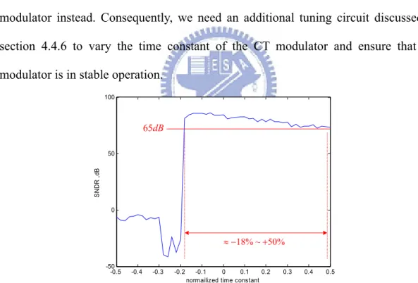
5.11 Simulated SNDR for -6 dBFS input under the variation of the time constant...63
5.12 Jittered SCR and NRZ waveform ...64
5.13 Comparison of the SCR and NRZ feedback for -6 dBFS input under the effect of the clock jitter ...64
5.14 Behavior model simulation result ...65
5.15 First and second stage integrators ...66
5.16 Implementation of the SCR feedback circuit...66
5.17 Operation amplifier and CMFB of the first stage ...68
5.19 Operation amplifier and CMFB of the second stage ...70
5.20 Frequency response of the second stage opamp ...70
5.21 (a) Differential-difference preamplifier (b) Low-offset regenerative latch ...71
5.22 (a) 17-level quantizer (b) Simulation result in time-domain ...72
5.23 (a) Low-jitter clock generator (b) Non-overlapping clock generator ...73
5.24 Simulation results of the non-overlapping clock generator ...73
5.25 (a) Active-RC integrator (b) Tuning circuit ...74
5.26 Wallace-Tree encoder...75
5.27 3-bit adder with carry lookahead ...76
5.28 Logic diagram of the DFF...77
5.29 Simulated operation of the edge-triggered DFF ...77
5.30 Simulated power spectral density of this work ...78
5.31 (a) Layout design (b) Die photo of this work ...80
6.1 Test setup………...82
6.2 Function generator hp 8656B for input signal ...82
6.3 Function generator ROHDE & SCHWARZ SML03 for clock...82
6.4 Logic analyzer Agilent 16902A ...83
6.5 Power supply regulator ...83
6.6 Single-to-differential transformer ...84
6.7 Reference voltage generator ...85
6.8 PCB of the CT modulator ...86
6.9 (a) Pin configurations (b) Pin assignments of the CT modulator ...86
6.10 PCB of the hybrid modulator...87
6.11 (a) Pin configurations (b) Pin assignments of the hybrid modulator ...87
6.12 Measured power spectral density of the CT modulator ...88
6.13 Post-simulation power spectral density of the CT modulator...89
6.14 Dynamic range plot of the CT modualtor ...89
Table Page
2.1 Properties of quantizers in Figs 2.5 and 2.6 ...9
3.1 Comparison with the main advantages of CT and DT SDM...22
3.2 S-domain equivalent for z-domain partial expansion...26
4.1 Zero placement for minimum in-band noise ...35
4.2 Performance of the first stage opamp ...44
4.3 Performance of the second and third stage opamp ...45
4.4 Truth table of the SR latch...46
4.5 Performance summary of this work...50
5.1 CT equivalences for DT loop filter with SCR feedback...60
5.2 Truth table of SCR DAC1 switches...66
5.3 Truth table of DAC2 switches ...67
5.4 Performance of the first stage opamp ...69
5.5 Performance of the second stage opamp ...71
5.6 Performance summary of this work...78
6.1 Measurement results of the CT modulator ...89
1.1 Motivation
Sigma-delta analog-to-digital converter (ADC) is traditionally used in instrumentation, voice, and audio applications that are low signal bandwidth and high resolution. In recent years, there has been a growing trend to move ADC towards the system front-end. This implies that more signal processing is shifted from analog domain to digital domain. Due to the scaling in VLSI technology, high performance digital systems can be realized. However, ADC has to provide higher dynamic range in the interface between analog and digital data. Therefore, sigma-delta ADC which can achieve high resolution with wide input bandwidth for wireless and wireline communication systems becomes more and more important [1] [2].
In sigma-delta ADC, the use of continuous-time (CT) loop filter provides several advantages over discrete-time (DT) implementations. Without critical slewing and settling issues, as in switched-capacitor circuits, CT integrators are often promised to achieve better power-performance efficiency [3]. Moreover, CT integrators are praised for better noise immunity due to their inherent anti-aliasing filtering which are especially advantageous in RF receivers [4]. However, CT integrators are sensitive to process variation thereby require extra tuning circuit to adjust the time constant. DT integrators, on the contrary, set the pole-zero locations by capacitor ratios, which are highly accurate. Another advantage of using DT loop filter is that its signal transfer function and noise transfer function scale with the clock frequency which could be
handy for a multi-standard system design. Alternative hybrid CT/DT loop filter approach tends to exploit the performance by keeping all the pros.
In this thesis, a CT single-bit active-RC sigma-delta modulator for Bluetooth application and a hybrid sigma-delta modulator with 60.6dB SNDR and 2MHz signal bandwidth are achieved. Various design techniques which are truncation error shaping, cancellation and switched-capacitor with resistive element (SCR) feedback are utilized to have better performance. The modulators with such specifications can be applied to Bluetooth and WCDMA wireless communication systems.
1.2 Thesis Organization
This thesis is organized into seven chapters.
Chapter 1 briefly introduces the motivation of the thesis.
Chapter2 first explains the performance parameters of the sigma-delta A/D and describes the background of the sigma-delta A/D conversion. Then, the concepts and advantages of quantization, oversampling and noise shaping are introduced. Finally, the common architectures of the sigma-delta modulator, single-loop and multi-stage, are illustrated and discussed.
Chapter 3 introduces the comparison of the CT and DT loop filter. Then, how to transform between the DT and the CT loop filter is described and the non-idealities of the CT modulator are explained.
Chapter 4 presents a continuous-time single-bit active-RC sigma-delta modulator for Bluetooth application. The design of the loop is illustrated, including the architecture and coefficients. The system and circuit level designs are introduced in detail. Non-idealities and important simulation results are included. Finally, in mixed-signal design, the considerations of the layout are discussed.
Chapter 5 presents the design of the hybrid sigma-delta modulator with digital error truncation. First, the principles of the truncation error shaping, cancellation and SCR feedback are introduced. The design considerations including non-idealities are analyzed in system level in order to implement a power- and area-efficient modulator in circuit level. Finally, the simulation results and layout design are presented.
Chapter 6 presents the testing environment, including the components on the printed circuit board (PCB) and instruments. The measurement results of the continuous-time single-bit active-RC sigma-delta modulator for Bluetooth application is shown and summarized.
Finally, the conclusions and the future works of this thesis are summarized in Chapter 7.
In this chapter, first, the performance parameters of the sigma-delta A/D are explained. Then we describe the background of the sigma-delta A/D conversion and introduce the concepts of quantization, oversampling and noise shaping. Finally, the common architectures of the sigma-delta modulator, single-loop and multi-stage, are illustrated and discussed.
2.1 Performance Parameters
There are commonly the most important performance parameters when sigma-delta A/D is compared. These performance parameters are described as follows:
2.1.1 Signal-to-Noise Ratio (SNR)
The signal-to-noise ratio of an A/D is the ratio of the signal power to the noise power over the interest band at the output of a converter. The theoretical value of SNR for sinusoidal inputs in a Nyquist rate A/D is given by
6.02 1.76
max
SNR = N+ (2.1) The derivation of the equation (2.1) is described in section 2.3.
2.1.2 Signal-to-Noise and Distortion Ratio (SNDR)
The signal-to-noise and distortion ratio of an A/D is the ratio of the signal power to the noise and all distortion power over the interest band at the output of a converter. In general, the SNDR is lower than SNR due to the distortion power.
2.1.3 Spurious Free Dynamic Range (SFDR)
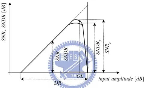
Spurious free dynamic range is defined as the ratio of the signal power to the maximum distortion component in the range of interest, as shown in Fig. 2.1.
[ ] f Hz [] M ag ni tud e dB 0 fin 2fin 3fin Signal Harmonics SF DR
Fig. 2.1 Performance of the SFDR
2.1.4 Dynamic Range (DR)
The dynamic range of an A/D for sinusoidal inputs is defined as the ratio of the maximum signal power to the signal power for a small input which the SNR is unity [5].
2.1.5 Effective Number of Bits (ENOB)
Equation (2.2) relates the number of bits to the SNDR used in an A/D when the input signal is a sinusoidal.
1.76 6.02
SNDR
2.1.6 Overload Level (OL)
Overload level is defined as the maximum input sinusoidal signal which the structure still operates correctly. Usually, the maximum stable amplitude is at the 6dB reduction of the peak SNR.
The performance parameters discussed above are summarized in Fig. 2.2, where
p
SNR and SNDR are the peak SNR and the peak SNDR, respectively [6]. p
SNR SN DR SN R SN D R dB [ ] input amplitude dB DR OL p SNR p SN DR
Fig. 2.2 Performance characteristic of a sigma-delta modulator
2.2 Sampling and Quantization
The conversion of analog signals to digital domain can simply be separated into two basic operations: sampling in time and quantization in amplitude.
Sample at the time Ts, or with a fixed frequency f , results in a periodicity of s
the original signal spectrum at multiples of f , as shown in Fig. 2.3. From Fig. 2.3, s
the original spectrum can be reconstructed by a simple low pass filter but the criterion known as Nyquist theorem
2
must be satisfied, where f is the signals of interest. Otherwise, the aliasing maybe B
occur, as shown in Fig. 2.4. In order to assure the condition in (2.3), an analog lowpass filter must be used to limit the signal bandwidth, called anti-aliasing filter. The ideal lowpass filter characteristic is called a brick wall response. However, in real implementations, the characteristic is impossibly to realize. On the contrary, the filter having n-pole roll-off in the transition band is easier to design and more inexpensive. We define the oversampling ratio (OSR) as
2 s B f OSR f = (2.4) It means that how much faster we sample in the oversampling converters than in a Nyquist rate converters. With higher OSR, the transition band of the anti-aliasing can be relaxed. s f 2fs 2fs - -fs 0 f ( ) S f LP filter B f B f
-Fig. 2.3 Spectral of the sampling operation
s f 2fs 2fs - -fs 0 f ( ) S f Aliasing
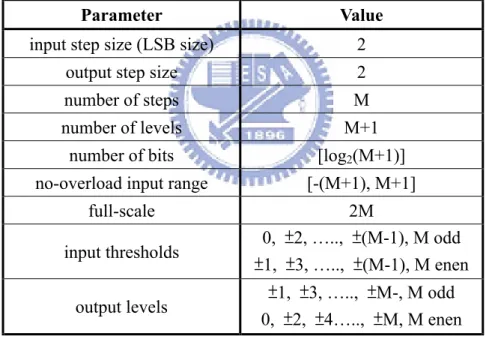
The process of quantization in amplitude encodes a continuous range of analog values into a set of discrete levels. The device which realizes the quantization is called a quantizer or ideal A/D converter. There are two types of the quantizers which are mid-rise and mid-tread [7], as shown in Figs. 2.5 and 2.6. In Fig. 2.5 (a), the mid-rise quantizer has u=0 in a rise of v . On the other hand, u=0 occurs in the middle of a flat portion of the curve and hence it is called a mid-tread quantizer. In ideal both cases, the straight line v ku= is the desirable A/D transfer curve, where the gain k
of the quantizer is determined by the ratio of the step size to the adjacent input thresholds known as the least-significant bit size (LSB size or D ). The deviation between the straight line v ku= and the real A/D characteristic is called quantization error or quantization noise. Figs. 2.5 (b) and 2.6 (b) illustrate the quantization error e . In the range from - -M 1 to M+1, the quantization error is within ±D . This 2 range is called no-overload input range and the difference between lowest and highest levels is named full scale (FS). Therefore, the FS is equal to
2N
FS= D × (2.5) where N is quantizer resolution. Table 2.1 summarizes the quantizers of the Figs 2.5 and 2.6. 2 (LSB size) D = =2 step size 2 4 6 M+1 4 -6 -1 M -1 3 5 M M -3 -5 -v ku= u v 2 4 6 M+1 4 -6 -1 M -1 3 5 M M -3 -5 -e v u= -2 -no overload input range -( )a ( )b u
4 6 1 M+ 4 -6 -1 3 5 M M -v ku= 2 3 -5 -1 M -v u 2 (LSB size) D = 2 step size = 4 6 1 M+ 4 -6 -1 3 5 M M -2 3 -5 -1 M -no overload input range -( )a ( )b e v u= -u
Fig. 2.6 M-step mid-tread quantizer (M is even) (a) transfer curve (b) error function
Table 2.1 Properties of quantizers in Figs 2.5 and 2.6
Parameter Value
input step size (LSB size) 2
output step size 2
number of steps M
number of levels M+1
number of bits [log2(M+1)]
no-overload input range [-(M+1), M+1]
full-scale 2M
input thresholds 0, ±2, ….., ±(M-1), M odd ±1, ±3, ….., ±(M-1), M enen
output levels ±1, ±3, ….., ±M-, M odd
0, ±2, ±4….., ±M, M enen
The basic A/D structure is shown in Fig. 2.7.
s f fs ( ) u t u n( ) v n( ) Anti - aliasing Filter S H/ Quantizer Analog Digital
2.3 White Noise
The quantizer can be modeled linearly as adding quantization error ( )e n in Fig.
2.8. If we assume that the input signal changes rapidly from sample to sample and the quantization error is independent of it, then the quantization error has equal probability density function (pdf) in the no-overload input range, as shown in Fig. 2.9 (a). The probability density function is
1 , ( ) ( ) 2 2 0 , Q e n f e otherwise -D D ì £ £ ï = Dí ïî (2.6) Therefore, it is possible to assume the quantization error to have statistical properties. A common assumption is that the quantization error has the following properties, usually referred to as the input-independent additive white noise approximation [8]:
Property 1 : ( )e n is statistically independent of the input signal or ( )e n is
uncorrelated with the input signal.
Property 2 : ( )e n is uniformly distributed in the no-overload input range.
Property 3 : ( )e n is an independent identically distributed sequence or ( )e n
has a flat power spectral density (PSD).
This assumption simplifies the analysis of an ADC system because a non-linear system is replaced by a linear one.
( ) e n ( ) u n v n( ) ( ) e n ( ) u n + v n( ) ( ) ( ) ( ) e n =v n -u n
e ( ) Q f e 2 D 2 -D 1 Q( ) 1 Height so that f e de ¥ -¥ = D = ò f ( ) e S f 2 s f 2 s f -0( ) e S f ( )a ( )b
Fig. 2.9 (a) Probability density function (b) Power spectral density of quantization noise
From Fig. 2.9 (a), we can calculate the total quantization noise power as: 2 2 2 ( ) 12 e e f e deQ ¥ -¥ D s =
ò
= (2.7) In (2.7), the quantization noise power is only related to the quantizer resolution and is independent of sampling frequency. In Fig. 2.9 (b), the power spectral density of the quantization noise is 2 1 ( ) 12 e s S f f D = (2.8) Assuming the input signal is a sinusoidal wave and using (2.5), its maximum amplitude A without clipping is 2 (N D . For this assumption, the signal power is 2)2 2 2 2 2 8 2 2 N N s P =æç Dö÷ = D è ø (2.9) Using (2.7) and (2.9), the SNR in Nyquist rate converters, which is the ratio of the signal power to the total quantization noise power, is calculated as follows:
2 2 3 10log 10log 2 6.02 1.76 2 N s max e P SNR = æç ö÷= æç ö÷= N+ s è ø è ø (2.10)
2.4 Oversampling
In (2.4), we have defined OSR. It represents how much faster the oversampling converters operate than the Nyquist rate converters. Oversampling can relax the requirement of the anti-aliasing filter, as shown in Fig. 2.10. In Fig 2.10, the transition band of the lowpass filter with oversampling is wider than without oversampling. The characteristic gives a favor in the design of anti-aliasing filter. Therefore, we don’t need a brick wall lowpass response. Instead of it, the filter having n-pole roll-off in the transition band is easier to design and more inexpensive.
From Fig. 2.10, due to the oversampling technique, the inband quantization noise is reduced. Consequently, the inband quantization noise power becomes
2 2 2 2 1 1 12 12 B f B e e s f s f P df f - B f OSR D D =
ò
s = = (2.11)Using (2.9) and (2.11), the SNR of a oversampling converters is as follows:
2 3
10log 10log 2 10log( )
2 6.02 1.76 10log( ) N s max e P SNR OSR P N OSR æ ö æ ö = ç ÷= ç ÷+ è ø è ø = + + (2.12)
Compared to (2.10), the SNR is enhanced by 3dB with doubling OSR. Therefore, the oversampling gives a SNR improvement with the OSR at a rate of 3dB/octave, or 0.5bit/octave. f ( ) S f f 2 s f 2 s f inband quantization noise ( ) S f B f B f inband quantization noise ( )a ( )b 2 s f 2 s f -B f B f -LP filter LP filter
2.5 Noise shaping strategy
The advantage of quantization noise shaping through the use of the feedback path is introduced in this section. With an additional feedback path, the different transfer functions can be obtained which are signal transfer function (STF) and noise transfer function (NTF).
A general noise shaping sigma-delta modulator (SDM) is shown in Fig. 2.11 (a), where H z is loop filter. Assuming the input signal and the quantization noise are ( ) independent signals discussed in section 2.3 and using 1-bit quantizer to simplify the analysis. The linear model of the modulator in z domain is shown in Fig. 2.11 (b). With this linear model, we can derive a STF and a NTF as defined
( ) ( ) ( ) ( ) 1 ( ) V z H z STF z U z H z º = + (2.13) ( ) 1 ( ) ( ) 1 ( ) V z NTF z E z H z º = + (2.14) According to (2.14), we can find out that the zeros of NTF z is equal to the poles ( ) of H z . It means that when ( ) H z go to infinity, ( ) NTF z will be zero. In other ( ) words, by choosing H z such that its magnitude is large in signal bandwidth, ( )
( )
STF z should approximate unity and NTF z should be close zero over the same ( ) bandwidth. For the output signal, we can express it in linear combination of the input signal and the noise signal in (2.15), which are filtered by STF and NTF, respectively.
( ) ( ) ( ) ( ) ( )
V z =STF z U z +NTF z E z (2.15) In general cases, the STF z has all-pass or lowpass frequency response and ( ) the NTF z has highpass characteristic. Based on (2.15), the inband quantization ( ) noise can be shaped to high frequency band and then it doesn’t affect the input signal [9]. Therefore, the SNR can be improved effectively by using noise shaping.
( ) H z -( ) u n v n( ) Quantizer + ( )a ( ) H z -( ) U z V z( ) + ( )b + ( ) E z
Fig. 2.11 (a) A general sigma-delta modulator (b) Its linear model in z domain
2.5.1 First-Order Sigma-Delta Modulator
From above discussion, for a first-order noise shaping, the NTF z should have a ( ) zero at dc (i.e., z=1), that is a lowpass frequency response, equivalently H z has a ( ) pole at dc. So the quantization noise has highpass characteristic. By letting H z be ( ) a discrete-time integrator, the function is
1 ( ) 1 H z z = - (2.16) where H z has a pole at dc (i.e., z=1). For this choice, the block diagram in z ( ) domain is shown in Fig. 2.12. In frequency domain, the STF z is given by ( )
1 1 ( ) 1 ( ) 1 ( ) 1 1 V z z STF z z U z z -º = = + (2.17)
and the NTF z is given by ( )
1 ( ) 1 ( ) 1 1 ( ) 1 1 V z NTF z z E z z -º = = -+ (2.18)
According to (2.15), the output signal becomes
1 1
( ) ( ) (1 ) ( )
-( ) U z V z( ) + + ( ) E z 1 z -+
Fig. 2.12 A first-order lowpass sigma-delta modulator
From (2.19), the STF z is just a delay while the ( ) NTF z is a discrete-time ( ) differentiator (i.e., a highpass filter). To estimate the inband quantization noise power, the squared magnitude of the NTF z needs to be found in frequency domain. By ( ) setting z e= j2pf fs , the NTF f becomes as follows: ( )
2 ( ) 1 2 2 sin( ) 2 s s s s s j f f j f f j f f j f f j f f s e e NTF f e j e j f j e f p - p - p - p - p -= - = ´ ´ p = ´ ´ (2.20)
Therefore, the squared magnitude of the NTF f is given by ( ) 2 2 ( ) 2sin( ) s f NTF f f é p ù = ê ú ë û (2.21) Using (2.8) and (2.21), the inband quantization noise power is
2 2 2 1 ( ) ( ) 2sin 12 B B f f e e s s f f f P S f NTF f df df f f B B - -é æ öù æD ö p = = ç ÷ ê ç ÷ú è ø ë è øû
ò
ò
(2.22)For frequencies which satisfy fB = (i.e., OSR>>1), fs ( )2 (2 )2 s
NTF f » p f f . By this approximation, we have [9]
2 3 3 2 1 2 2 2 2 2 1 2 12 12 3 36 B f B e s s s f f f P df f f f OSR B -é æ öù æ ö æD ö p æD öæp ö D p æ ö = ç ÷ ê ç ÷ú =ç ÷ç ÷ç ÷ = ç ÷ è ø è ø ë è øû è øè øè ø
ò
(2.23)According to (2.9), the SNR for this case is given by
(
)
3 22
3 3
10log 10log 2 10log
2 6.02 1.76 5.17 30log( ) N s max e P SNR OSR P N OSR æ ö æ ö é ù = ç ÷= ç ÷+ ê ú p è ø ë û è ø = + - + (2.24)
With doubling OSR, the SNR performance is improved by 9dB, i.e., 1.5bit/octave. Compared to (2.12), the SNR has the improvement of 1bit/octave.
2.5.2 Second-Order Sigma-Delta Modulator
To realize a second-order sigma-delta modulator, the NTF z should be a ( ) second-order highpass function. The block diagram of the modulator is shown in Fig. 2.13. For this modulator, the STF z is given by ( )
STF z( )=z-1 (2.25) and the NTF z is given by ( )
(
1)
2( ) 1
NTF z = -z- (2.26) Similarly, we are interested in the squared magnitude of the NTF z . It is ( )
4 2 ( ) 2sin( ) s f NTF f f é p ù = ê ú ë û (2.27) Using the same assumption OSR>>1, the quantization noise power over the frequency band of interest becomes
5 5 2 4 2 4 2 2 1 ( ) ( ) 12 5 60 B f B e e s f f P S f NTF f df f OSR B -æ ö æD öæp ö D p æ ö = =ç ÷ç ÷ç ÷ = ç ÷ è ø è øè øè ø
ò
(2.28)Again, according to (2.9), the SNR for this case is given by
(
)
5 24
3 5
10log 10log 2 10log
2 6.02 1.76 12.9 50log( ) N s max e P SNR OSR P N OSR æ ö æ ö é ù = ç ÷= ç ÷+ ê ú p è ø ë û è ø = + - + (2.29)
With doubling OSR, the SNR performance is improved by 15dB, i.e., 2.5bit/octave. Comparison with different noise shaping transfer functions which are zero-, first- and second-order is shown in Fig. 2.14. In signal bandwidth f , we can B
see that the quantization noise power decreases as the noise shaping order increases, as discussed above. -( ) U z V z( ) + + ( ) E z 1 z -+ + 1 z -+
-Fig. 2.13 A second-order lowpass sigma-delta modulator
0 0.05 0.1 0.15 0.2 0.25 0.3 0.35 0.4 0.45 0.5 -80 -70 -60 -50 -40 -30 -20 -10 0 10 20 Normalized Frequency |N TF (z )|, dB no noise shaping First-order Second-order fs/2 fB no noise shaping First-order Second-order
2.5.3 Higher-Order Sigma-Delta Modulators
Fig. 2.18 shows the block diagram of the L-order sigma-delta modulator. As the first- and second-order SDM, the NTF z of the L-order SDM should be chosen to ( ) have an L-order highpass function. This gives
1
( ) (1 )L
NTF z = -z- (2.30) In the same manner and assumption, we can find out the inband quantization noise power is 2 1 2 1 2 2 2 2 2 1 12 2 1 12(2 1) L L L L B e s f P L f L OSR + + æ ö æD öæ p ö D p æ ö »ç ÷ç ÷ç ÷ = ç ÷ + + è ø è øè øè ø (2.31)
Therefore, the maximum SNR for this case is given by
(
)
2 1 22
2
3 2 1
10log 10log 2 10log
2 6.02 1.76 10log (20 10) log( ) 2 1 L N s max L e L P L SNR OSR P N L OSR L + æ ö æ ö é + ù = ç ÷= ç ÷+ ê ú p è ø ë û è ø æ p ö = + - ç ÷+ + + è ø (2.32)
From (2.32), the SNR performance can be improved by (6L+3) dB with doubling OSR, or at a rate of (L+0.5) bit/octave. However, higher than second-order SDM suffers from potential instability due to the accumulation of large signals in the integrators. Consequently, stability problems reduce the achievable resolution to a lower value than the equation (2.32).
-( ) U z V z( ) + + ( ) E z 1 z -+ + 1 z -+ - -+
2.5.4 Multi-Stage Modulators
Another realization of the higher order SDM is the cascade modulator, also called the multi-stage or MASH (Multi-stAge noise-SHaping) modulator. The MASH modulator is constructed from lower order SDMs. Therefore, it can ease the stability problems. The basic second-order block diagram is illustrated in Fig. 2.16. The output signal of the first stage is given by
1 1
1( ) 1( ) ( ) 1( ) ( )1 ( ) (1 ) ( )1
V z =STF z U z +NTF z E z =z U z- + -z- E z (2.33)
where STF z and 1( ) NTF z are signal transfer function and noise transfer function 1( ) of the first stage, respectively. From Fig. 2.16, the input signal of the second stage is the quantization noise of the first stage E z . Therefore, the output signal of the 1( ) second stage is given by
1 1
2( ) 2( ) ( )1 2( ) ( )2 1( ) (1 ) ( )2
V z =STF z E z +NTF z E z =z E z- + -z- E z (2.34)
where STF z and 2( ) NTF z are signal transfer function and noise transfer 2( ) function of the second stage, respectively. The digital filter H z and 1( ) H z are 2( ) designed to cancel the quantization noise E z of the first stage in the overall 1( ) output ( )V z . By using (2.33) and (2.34), the condition is
1 1
1 2
(1-z- )H z( )-z H z- ( ) 0= (2.35)
The simplest choices for H z and 1( ) H z are 2( ) 1 1( )
H z =z- and 1
2( ) (1 )
H z = -z- . So, the overall output is given by
2 2 2
2
( ) ( ) (1 ) ( )
Therefore, the second-order MASH modulator has second-order noise shaping but the stability behavior is first order one. However, if the condition (2.35) is not satisfied due to the imperfection of the analog and digital transfer functions, the SNR performance is degraded greatly.
( ) U z V z1( ) + 1( ) E z 1 z -+ + -1 bit DAC + -+ 2( ) E z 1 z -+ + -1 bit DAC 1( ) E z 2( ) V z 1( ) H z 2( ) H z + -( ) V z Analog Digital
Fig. 2.16 A second-order MASH modulator
2.6 Summary
In this chapter, performance parameters of a sigma-delta modulator are first explained. Then, we introduce the basic concept of the SDM and the fundamental principles of how a modulator works are described. Through the use of oversampling and noise shaping, the SNR performance can be improved in the band of interest. Finally, the common architectures of the SDM, single-loop and multi-stage, are illustrated and discussed.
3.1 Discrete-Time / Continuous-Time Modulators
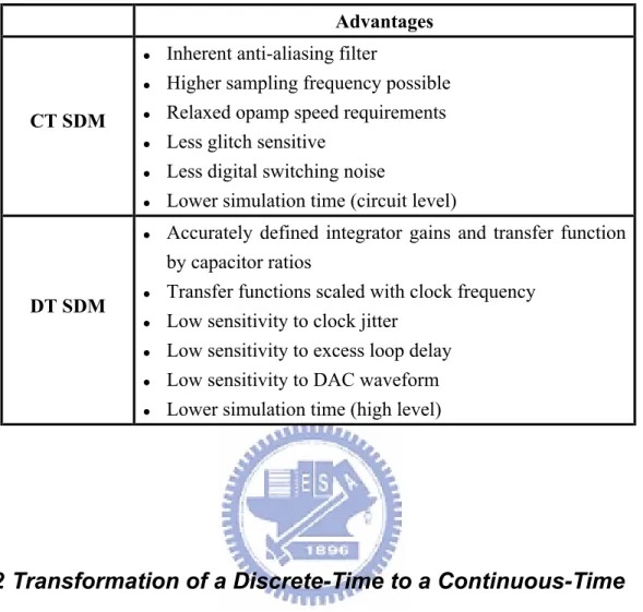
Sigma-delta A/D converters are widely used in wireless and wireline communication system. In recent years, continuous-time (CT) sigma-delta A/D gains growing interest in wireless application for their lower power consumption and wider input bandwidth as compared to the discrete-time counterparts. In other words, the opamp of CT SDM can be relaxed at speed requirements or CT SDM can operate at higher sampling frequency. Moreover, CT SDM is praised for better noise immunity due to their inherent anti-aliasing filtering which are especially advantageous in RF receivers [4]. Besides, the absence of the switches makes CT SDM has less glitch and less digital switching noise.
DT SDM, on the contrary, is insensitivity to clock jitter and exact shape of opamp settling waveform as long as full settling occurs. Another advantage of DT SDM is that the integrator gain and transfer functions are accurately defined.
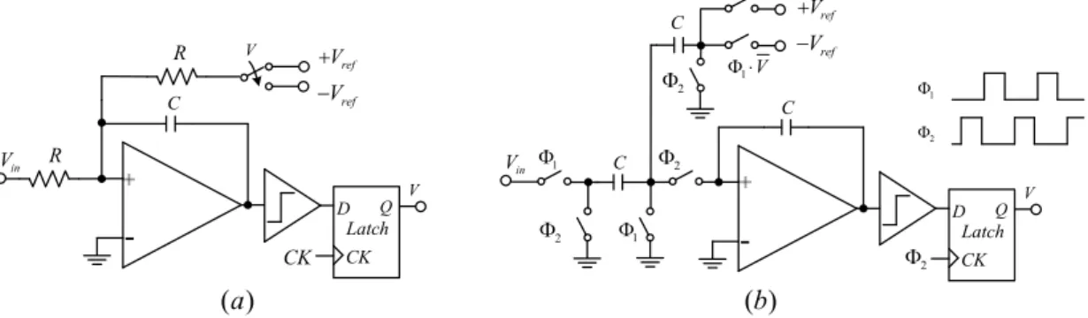
The main advantages of CT and DT SDM are summarized in Table3.1 and their block diagrams are shown in Fig. 3.1 [6] [8].
2 F 1 F C 1 F C 2 F in V F2 1 F DLatch CK Q 2 F C 2 F V 1 1V F × ref V + ref V -CK in V V R R ( )a ( )b D Latch CK Q V C ref V + ref V
Table 3.1 Comparison with the main advantages of CT and DT SDM
Advantages
CT SDM
l Inherent anti-aliasing filter
l Higher sampling frequency possible l Relaxed opamp speed requirements l Less glitch sensitive
l Less digital switching noise
l Lower simulation time (circuit level)
DT SDM
l Accurately defined integrator gains and transfer function
by capacitor ratios
l Transfer functions scaled with clock frequency l Low sensitivity to clock jitter
l Low sensitivity to excess loop delay l Low sensitivity to DAC waveform l Lower simulation time (high level)
3.2 Transformation of a Discrete-Time to a Continuous-Time
In section 3.1, we have introduced why the CT SDM gains growing interest. Due to the widely used sigma-delta toolbox [7], the DT loop filter can be obtained easily. By contrast, the loop filter design of a CT SDM is nontrivial because it has a strong dependence on the pulse shape of the feedback digital-to-analog converter (DAC). Fortunately, we can find a CT loop filter through the equivalent DT loop filter and transforming it to continuous-time.
Fig. 3.2 shows a CT and a DT SDM, respectively. In DT SDM, the sampling is at the front-end input while it is at the input of the quantizer in CT SDM. If they have the same output sequences in the time domain for the same time instants, they can be considered equivalent. This is shown in Fig. 3.3 (a) and (b) which are open-loop of
the CT and DT SDM. As mentioned above, the criterion for the two equivalent modulators is ( ) ( ) | s t nT x n =x t = (3.1) This can be satisfied if their impulse responses are equal at each sampling instants. This results in the condition [10]
{
( )}
1{
( ) ( ) |}
s DAC t nT H z L H s H s -1 -= Z = (3.2)or, in the time domain [11]
[
]
( ) DAC( ) ( ) |t nTs DAC( ) ( ) |t nTs h n h t h t h t h t t td ¥ = = -¥ = * =ò
* - (3.3)where hDAC( )t is the impulse response of the DAC. The transformation between CT
and DT is called the impulse-invariant transformation. Although forward Euler integration, back Euler integration, bilinear transformation and midpoint integration are known and popular in linear filter designs for transformation between DT filters and CT filters. However, they are not suitable for transforming between DT SDM and CT SDM. The reason is that SDM is essentially a non-linear system. Thus, the impulse-invariant transformation is the most proper method to transform DT modulators to CT modulators. -( ) u t v n( ) + H s( ) DAC ( ) x t ( ) v t ( ) x n 1 s s f T = -( ) u n v n( ) + H z( ) DAC ( ) x n ( )a ( )b
DAC H s( ) ( ) x t x n( ) 1 s s f T = ( ) v n v t( ) DAC H z( ) x n( ) ( ) v n v t( ) t t ( )a ( )b
Fig. 3.3 Open-loop (a) CT (b) DT sigma-delta modulator
According to (3.2) and (3.3), different DAC feedback pulse shape results in different transformation between DT modulators and CT modulators. In consequence, before doing this transformation, the pulse shape has to be selected first. There are three commonly used rectangular DAC feedback pulse shapes which are non-return-to-zero (NRZ), return-to-zero (RZ) and half-delay-return-to-zero (HRZ) [12], as shown in Fig. 3.4. For simplicity, the magnitudes of the rectangular DAC pulses are assumed to be 1 and in the time domain, this is given by
1, , 0 1 ( ) 0, DAC t h t otherwise a £ <b £ < £a b ì = í î (3.4)
where a and b are feedback starting and ending times. So, the three rectangular DAC feedback pulses are
0, 1 0, 0.5 0.5, 0 NRZ RZ HRZ a b a b a b = = ì ï = = í ï = = î (3.5)
By the Laplace transform of (3.4), their responses in s-domain can be described as follows exp( ) exp( ) ( ) DAC s s H s s a b - - -= (3.6)
s T 2 s T 0 1 NRZ RZ HRZ ( )a ( )b ( )c
t
1 1 s T 2 s T 0t
0 Ts 2 Tst
Fig. 3.4 DAC feedback pulse shapes (a) NRZ (b) RZ (c) HRZ
After determining the DAC feedback pulse shape and its response, impulse-invariant transformation can be used in following steps. First, we need to express the H z as a partial fraction expansion and then convert each partial ( ) fraction expansion from z-domain to s-domain. Finally, the H s can be derived by ( ) recombining the results.
Table 3.2 lists the results of impulse-invariant transformation between CT loop filters and DT loop filters for the commonly used DAC feedbacks [13].
Table 3.2 S-domain equivalent for z-domain partial expansion z-domain partial fraction s-domain equivalent General z k 1 1 k k s k s z - sT -s NRZ 1 k z = 1 s sT General z k k 0.5 1 k k s k s z -z sT -s RZ 1 k z = 2 s sT General z k 0.5 1 1 k k s k s z - sT -s 1 1 1 k z z z -HRZ 1 k z = 2 s sT General z k 2 2 2 ( 1 1 ) 1 ( 1) ( ) k k s k k s k s z sT s z sT s - + - -- -NRZ 1 k z = 1 2 0.5 (sTs) -sTs General z k 0.5 0.5 0.5 2 0.5 2 2 (0.5 1) 1 (0.5 1) 1 ( ) ( ) k k k s k k k k s k z s z sT z s z z sT s - - -é - + - ù + -ë û - -RZ 1 k z = 1.5 2 2 ( ) s s sT sT - + General z k 0.5 0.5 1 0.5 2 0.5 2 2 ( 0.5 ) 0.5 1 ( 1) ( ) k k k k s k k k s k z s z z sT z s z sT s - - - -- + - -- -2 1 2 (1 k ) z z z -HRZ 1 k z = 0.5 2 2 ( ) s s sT sT - +
3.3 Non-idealities of Continuous-Time Modulators
In this section, non-idealities of CT modulators, including opamp in CT integrators, excess loop delay and clock jitter, are explained. These different non-idealities can cause different effects which are performance degradation or even making modulators unstable. Through understanding of these non-idealities and modeling their behaviors in system level simulations, we can analyze and overcome them in circuit level.
3.3.1 Opamp in CT Integrators
For a typical active-RC integrator shown in Fig. 3.5, the ideal transfer function is 1
out in V
V = -sRC (3.7)
where R is the input resistor and C is the integration capacitor.
In presence of finite DC gain A and by assuming 0 A0 >> , the transfer 1 function becomes 0 1 1 out in V V » -sRC+ A (3.8) Considering the finite DC gain, gain bandwidth and only the dominant pole of the opamp, the transfer function can be expressed as
0 1 (1 ) out s s in V f f V s GBW A a a » -× × + + (3.9) where a is the scaling coefficient, f is sampling frequency while s GBW and A 0
Fig. 3.5 A fully differential integrator with finite gain and bandwidth
Through the equation (3.9), we can analyze the requirement of the opamp in CT integrators in system level and design power-efficient CT modulators in circuit level.
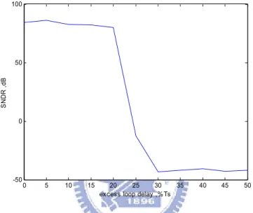
3.3.2 Excess Loop Delay
Ideally, the feedback DACs respond immediately to the quantizer clock edge, but in practice, the quantizer of the sigma-delta modulators has non-zero time to generate the correct outputs. The time including quantizer delay and the response time of the feedback DAC is called excess loop delay as illustrated in Fig.3.6 [12].
s
T
t
t
dT
st
Fig. 3.6 Excess loop delay for NRZ DAC pulse
The excess loop delay can cause the deviation of the transfer function or even the modulator unstable. For example, supposing a second-order CT modulator has the transfer function: 2 1 1.5 ( ) s H s s + = - (3.10)
s
T
t
dt
t
dT
st
T
st
dt
=
+
Fig. 3.7 Delayed NRZ pulse as a linear combination
We select the NRZ feedback DAC pulse and assume that the excess loop delay is t d as shown in Fig 3.6. It is possible to write the delayed NRZ pulse as a linear combination as shown in Fig. 3.7.
( ,1d d)( ) ( ,1)d ( ) (0, )d ( 1)
ht +t t =ht t +h t t- (3.11) By using impulse-invariant transformation to transform CT loop filter to DT loop filter, the DT transfer function is
2 2 2 2 2 ( 2 2.5 0.5 ) (1 4 ) (1.5 0.5 ) ( , ) ( 1) d d d d d d d z H z z z t t t t t t t = - + - + - + + -- (3.12)
Letting t = , the transfer function becomes d 0
2 2 1 ( ) ( 1) z H z z - + = - (3.13) as it should. If we design t = on purpose, the result is d Ts
1 2 2 1 ( ) ( 1) z H z z z - - + = × - (3.14) It is just a delayed version of (3.13). Therefore, the block diagram of the modulator can be shown in Fig. 3.8. However, due to the full clock delay, the design results in that the impulse response is zero at the first sampling instant Ts. To compensate the
response, an extra feedback branch is added directly to the front of the quantizer as shown in Fig. 3.9. Because the extra branch includes no integrators, the loop is called
by zero-order loop. Consequently, with the method, we can modify the modulator slightly and overcome the non-ideality of the excess loop delay.
( ) u t 1 v n( ) s -+ 1 s 1 z --+ k1 k2
Fig. 3.8 Second-order CT modulator with t = d Ts
( ) u t 1 v n( ) s -+ 1 s 1 z --+
k
1k
2 -+ 1 f kFig. 3.9 Modified second-order CT modulator
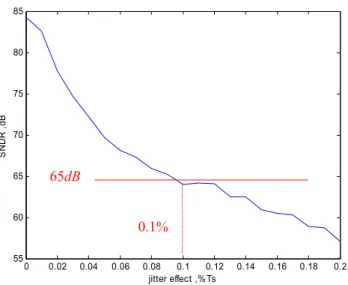
3.3.3 Clock Jitter
In CT sigma-delta modulators, one of the most important non-idealities is clock jitter. The clock jitter arises from both the quantizer and the feedback DACs. Due to the same order noise shaping, the sampling error at the quantizer only adds little noise to the modulator output. Nevertheless, the clock jitter in the feedback DACs generates non-shaped noise. It is the primary reason to affect the modulator performance significantly.
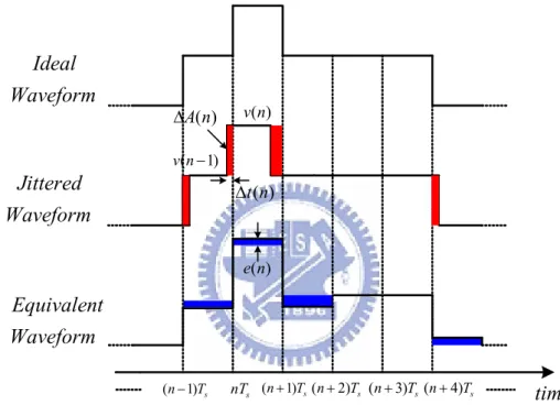
Fig. 3.10 shows the model of the jitter-induced noise for NRZ feedback DAC. In each sampling instant, the error area DA n( ) between ideal waveform and jittered waveform can be modeled as an equivalent error in the signal magnitude ( )e n . In
other words, the equivalent error ( )e n can be expressed as follows
(
)
( ) ( ) ( ) ( ) ( 1) s s A n t n e n v n v n T T D D = = - - × (3.15) From (3.15), we can observe that if the difference between (v n- and ( )1) v n is less,the clock jitter has lees effect upon the modulator performance. Therefore, the multi-bit quantizer has better jitter noise immunity.
s nT (n-1)Ts (n+1)Ts(n+2)Ts (n+3)Ts(n+4)Ts Ideal Waveform Jittered Waveform Equivalent Waveform time ( ) v n ( 1) v n -( ) A n D ( ) e n ( ) t n D
Fig. 3.10 Model of the jitter-induced noise for NRZ feedback DAC
DAC shape also affects the jitter sensitivity of CT modulators. This can be illustrated by Figure 3.11, where single-bit NRZ, RZ and HRZ feedback DAC shapes are described. In Fig. 3.11, the solid lines indicate the affected clock edges. In NRZ aspect, the NRZ DACs are only affected by clock jitter when the outputs change. On the contrary, the RZ and HRZ DACs suffer from the effect of the clock jitter in rising and falling edges of every clock cycle. They are more frequently affected than NRZ. So, the NRZ DAC is more resistant to the clock jitter. A good rule of thumb is that CT modulators employing RZ or HRZ DACs experience jitter noise about 6dB worse in
the signal band than if NRZ DACs are used [12]. s nT (n-1)Ts (n+1)Ts(n+2)Ts (n+3)Ts(n+4)Ts NRZ RZ HRZ time
4.1 Introduction
In this chapter, we implement a continuous-time single-bit active-RC sigma-delta modulator for Bluetooth application. The order of the loop filter is third and through the use of the architecture, cascade of resonators with distributed feedback (CRFB) [7], we can improve the bandwidth without increasing the order of the loop filter.
We use the typical type, active-RC integrator, to implement the first, second and third stage. Due to the closed-loop operation, the active-RC integrator has better linearity than the gm-C integrator. However, because of the loading effect, the
active-RC integrator requires an additional output buffer which consumes much power. This is a trade off between the two typical integrators.
Finally, the system and circuit level implementations are presented and the design considerations are explained. The chip is designed in TSMC 0.18μm CMOS process and the chip size is 1.32mm x 1.23mm. This work achieves 69.5dB SNDR performance and consumes 21.9mW at 1.8V supply voltage.
4.2 Loop Filter Architecture
4.2.1 Architecture
The loop filter of the CT third-order modulator uses CRFB architecture, as shown in Fig. 4.1. The transfer function in Fig. 4.1 can be derived by
0 0.5 1 1.5 2 2.5 3 3.5 x 10⁶ -150 -100 -50 0 Frequency, Hz P S D , dB 2 3 3 2 3 2 1 2 3 1 3 2 3 ( ) ( ) a c s c c a s c c c a H s s g c c × × + × × + × × × = + × × (4.1) The advantage of the architecture is capable of realizing NTF zeros as two conjugate complex pairs on the unit circle to obtain wider bandwidth. For example, the pole-zero plot of the third-order architecture is illustrated in Fig. 4.2. In Fig. 4.2, we can observe that there are one zero at DC and two conjugate zeros on the unit circle as the described advantage. The power spectral density is shown in Fig. 4.2 (a).
It is expected that even greater benefits can be obtained by optimizing the location of the zeros of higher-order NTF. The resulting values for the zeros are given in Table 4.1 for NTF with degrees from 1 to 8 [7].
u -1 s 1 c -1 s 2 c -1 s 3 c g -DAC 1 a a2 a3 v Fig. 4.1 CRFB architecture
Table 4.1 Zero placement for minimum in-band noise
N Zero locations, normalized to bandwidth wB SNR improvement
1 0 0 dB 2 ±1 ( 3) 3.5 dB 3 0, ± 3 5 8 dB 4 ± 3 7± (3 7)2-3 35 13 dB 5 0, ± 5 9± (5 9)2-5 21 18 dB 6 ±0.23862, 0.66121, 0.93247± ± 23 dB 7 0, 0.40585, 0.74153, 0.94911± ± ± 28 dB 8 ±0.18343, 0.52553, 0.79667, 0.96029± ± ± 34 dB
4.2.2 Coefficients
One of the most important designs in sigma-delta modulator is the coefficients. Different coefficients have different noise shaping and stability issues. Fortunately, by the widely used sigma-delta toolbox [7], the DT loop filter can be obtained easily. For example, the synthesizeNTF function in sigma-delta toolbox is used to synthesize a NTF according to the order of the modulator, OSR and so on. In other words, we can obtain the STF and the loop filter function from the NTF. Therefore, through the use of the impulse-invariant transformation introduced in section 3.2, the CT loop filter function can be derived.
For example, first, by using the synthesizeNTF function and assuming the third-order lowpass modulator, where the OSR is equal to 50 and the maximum out-of-band gain of the NTF is 1.7, the DT NTF can be derived by
2 2 ( 1)( 1.998 1) ( ) ( 0.5932)( 1.37 0.5824) z z z NTF z z z z - - + = - - + (4.2)
and the DT loop filter can be expressed as 2 2 1.0349( 1.549 0.6325) ( ) ( 1)( 1.998 1) z z H z z z z - + = - - + (4.3) Second, by applying impulse-invariant transformation in Matlab, the CT loop filter can be obtained by 2 3 0.8306 0.3804 0.0864 ( ) 0.002 s s H s s s + + = + (4.5) Finally, from (4.1), (4.5) and by assigning the initial values of the feedback coefficients a1 = , 1 a2 = and 1 a3 = , the CT coefficients can be acquired as 1
1 0.2272, 2 0.458, 3 0.8306, 0.0053
c = c = c = g= (4.6)
This is not the only solution and many other more systemic methods proposed in [7] can also effectively resolve the coefficient issues.
4.3 System Level Analysis
The first step of design sigma-delta modulator is to determine the NTF. By the sigma-delta toolbox, the NTF can be easily derived according to the specifications. In this work, we design a third-order modulator, where the OSR is equal to 50 and the maximum out-of-band gain of the NTF is 1.7, as shown in Fig. 4.3. In Fig. 4.3 (a), we simulate the maximum out-of-band gain of the NTF versus the peak SNR in system level. Due to the stability issue, we can find that the maximum out-of-band gain of the NTF is limited. The plot of the input level versus the SNR is shown in Fig. 4.3 (b). Therefore, we choose that the maximum out-of-band gain of the NTF is equal to 1.7 and the peak SNR is 86dB.
Fig. 4.3 (a) Maximum out-of-band gain of the NTF versus the peak SNR (b) Input level versus the SNR in system level
Based on the architecture of Fig. 4.1, the SIMULINK model of the system level is shown in Fig. 4.4. By the SIMULINK model, we can analyze different non-idealities to estimate the noise budget and achieve attainable performance.
The CT third-order sigma-delta modulator operates at 100MHz and the signal bandwidth is 1MHz. The oversampling ratio is equal to 50.