rail. TG2 belongs to different control loops depending on input signal C. If C = 0 the control loop is created by TG2 and TG3. As the transmission gate receives C = 0, it is open and the control loop is in a floating state. Otherwise, if C = 1, TG2 belongs to the control loop created by TGI and TG2. In this case the module driving TGI is disconnected, so the control loop is then also in a floating state. Thus, for both values of input signal C, the bridged node belongs to a control loop in a floating state, it may be a state modifying bridge and the sizing of the transistors has to be consid- ered. In the example, the sizing of transistors makes the faulty cir- cuit IDDp undetectable. Similar analyses are carried out for the remainder of the state modifying bridges and they have been detected by a voltage-based test methodology.
a
Fig. 3 Example of a realistic state modrfymg bridge in the scan-path FF
In the example, for
R,
greater than 2kQ, the bridges do not have any state modifying behaviour and, consequently, are IDDa testable.Conclusions: In sequential CMOS circuits control loops may be used to implement memories. These structures may introduce an undesired evolution of their signals if bridging defects are present. It has been shown that irredundancy is not a sufficient condition for current detectability of these CMOS sequential defective cir- cuits affected by bridges. However, every time a control loop is not current testable, an erroneous logic value and a voltage logic test may he applied. A simple example of a scan-path FF has been studied and 8.1% of realistic bridges (shorts, R, = 0) has been found to modify the memorised state. For bridge resistance greater than 2R, all bridges were lDoa detectable.
Acknowledgments: This work has been partially supported by the Project ARCHIMEDES (ESPRIT111 Program BRA, No 7107) and by the CICYT No TIC 1024190.
0 IEE 1993
Electronics Letters Online No: 1YY4001 7
R. Rodriguez-Montanes and J . Figueras (Universitat Polirecnica de Calalunya Deparfament d’Enginyeria Electrdnica Diagonal 649, Planta 9, 08028 Barcelona, Spain)
27 October IYY3
References
LEVI, M.W.: ‘CMOS is most testable‘. Int. Test Conf., 1981. pp. 217 220
SODEN, J.M., HAWKINS, C.F., GULATI, R . K , and MAO. W : ‘low testing: A review’, J. Electron. Testing: Theory and Applications, December 1992, 3, (4), pp. 291-303
SHEN, J.P., MALY, w., and FERGUSON. F.J.: ‘Inductive fault analysis of MOS integrated circuits’, lEE€ Design and Test, December 1985, pp. 13-26
NIGH, P., and MALY, w.: ‘Test generation for current testing’, I€€€ Design and Test of Computers, 1990, pp. 26-38
MILLMAN, S.D., and MCCLUSKEY. E.J : ‘Detecting bridging faults with stuck-at test sets’. Int. Test Conf., 1988, pp. 773-783
circuits to facilitate I,,, testing of bridging faults’, I€€€ Trans., May 1992, CAD-11, (3, pp. 659-670
LEE, K.J., and BREUER, M.A.: ‘Design and test rules for CMOS
Low-voltage BiCMOS dynamic minimum
circuit using a parallel comparison algorithm
for fuzzy controllers
J.B. Kuo, J.Y.
Wang and Y.G. Chen
lndering term.%: Fuzzy conrrol. BiCMOS integrated circuits The Letter presents a low-voltage BiCMOS dynamic minimum circuit using a parallel comparison algorithm for VLSI implementation of fuzzy controllers. Using low-voltage BiCMOS dynamic circuits [ I ] and a parallel comparison algorithm, a four- 4-bit-input minimum circuit designed, based on a 1 pn BiCMOS technology, shows a 9.5ns comparison lime, which is a x2.5 improvement in speed as compared to that based on CMOS technology.
Introduction; Fuzzy controllers that mimic human behaviour have been successfully applied to replace traditional control systems. In a fuzzy controller. the most important part is the inference engine, which is mainly composed of minimudmaximum circuits. Mini- mum/ maximum circuits using various CMOS circuits have been reported [2, 31. Recently, BiCMOS technology is becoming a major tool for building VLSI systems owing to its superior advan- tages in speed performance. A minmium circuit [4] using a BiC- MOS dynamic circuit [SI and a parallel comparison algorithm for fuzzy controllers was reported. For advanced BiCMOS technolo- gies, scaling power supplies is unavoidable [ 6 ] . For a deep sub- half-micrometre BiCMOS technology, a 1.5V supply is necessary. With a 1.5V supply, the BiCMOS dynamic circuit introduced before cannot be used. In this Letter, using low-voltage BiCMOS dynamic digital circuits [I], a low-voltage BiCMOS dynamic mini- mum circuit suitable for realising large-scale fuzzy controllers is described.
bit 4 bit 3
K)66111 Fig. 1 Black diagram offour-4-bit-input minimum circuit
Circuir: Fig. 1 shows the block diagram of the four-4-bit-input minimum circuit using low-voltage BiCMOS dynamic circuits and a parallel comparison algorithm. For selecting the minimum of four 4-bit inputs ( l ~ 4 1 , , l , J , , , i = l,4), instead of comparing two at a time. four inputs are compared at the same time from MSB (j = 4) to LSB (j = I ) using the the parallel comparison algorithm:
4
Ollt,
=UCCA
. ~ e / ~ , ~ + ~ ) j = 4 , l (1) t = 1 , 4 j = 4, 1 ( 2 ) Sc1,,5 = 1 I = 1 . 4 (3) i = 1 Sc/,,, = SC/,,,~+~ v[Iz,,
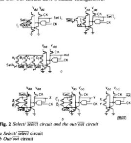
A-)where I,., is t h e j t h bit of the ith input. Each cell contains Select1 377Z and O u t 1 0 2 circuits to realise eqns. 1 and 2. As shown in Fig. 2u, during the precharge period, the outputs of both the Select and the SEi circuits are precharged to high. After the pre- charge period, the outputs may be pulled down and stay high
ELECTRONICS LETTERS 6th January 1994 Vol.
30
No. 1
31
~~
I
according to the specific input logic states. As shown in Fig. 26, the O u r l O 2 circuits have a similar configuration.
vdd ydd
‘dd ‘dd
’dd vdd ”dd ‘dd ‘dd ‘dd
h
Fig. 2 Select/ E‘Z circuit and the out/oUt circuit a Select/ E’Z circuit
b Our/oUt circuit
As in a pipelined system, cascading dynamic logic gates may have serious race problems. In the minimum circuit using the low- voltage BiCMOS dynamic logic circuit, no race problems exist because the operation of the BipMOS pulldown structure is a ‘buf€er’ instead of an ‘inverter’.
IF323 Fig. 3 Layout of low-voltage BiCMOS dynamic and CMOS static minimum circuits
cuit and the 1.5V CMOS static circuit based on a lpm BiCMOS technology, which has a gate oxide thickness of ISOA, a threshold voltage of +0.7V and a bipolar device with a unity gain frequency of SGHz, has been designed. The aspect ratios of all nMOS and PMOS devices used are 3 6 W 1 pm and W p d l pm, respectively. Fig. 3 shows the layout of the 1.5V BiCMOS dynamic circuit and the CMOS static circuit. The die areas of the dynamic and CMOS static circuits are 755 x 919pm2 and 609 x 959pm2, respectively. Fig. 4 shows the transient waveform of the four-4-bit-input mini- mum circuit using 1.5V BiCMOS dynamic and CMOS static cir- cuits. The propagation delay of the BiCMOS dynamic circuit is 9.5ns, which is 2.5ns less as compared to that of the CMOS static circuit. In addition, the 1.5V BiCMOS dynamic minimum circuit using a parallel comparison algorithm has an expansion capability to realise large-scale minimum circuits: 4 bit inputs using five four- 4-hit-input minimum circuits. Compared with the conventional minimum circuit that does not use the parallel comparison algo- rithm, this BiCMOS dynamic minimum circuit is much more com- pact.
0 IEE 1993
Electronics Letters Online No: 19940070
J.B. Kuo, J.Y. Wang and Y.G. Chen (Rm. 338, Dept. of Elec. Eng., National Taiwan University, Roosevelt Rd. Sec. 4, Taipei 106-17. Taiwan)
IO November 1993
References
1 KUO, J.B., CHEN. S.S., CHIANG. C . S . , SU. K.W., and LOU. J.H.: ‘A 1.5V BiCMOS dynamic logic circuit using a ’BiPMOS pull-down’ structure for VLSI implementation of full adders’, to be published in IEEE Trans. Circuits and Systems
2 WATANABE, H., DETTLOFF. w.D.. and YOUNT, K.E.: ‘A VLSI fuzzy logic controller with reconfigurahle, cascadable architecture’, IEEE J. Solid State Circuits, 1990, pp. 37tS380
SASAKI, M., [ N o w . T., sHiRAi, Y., and UENO, F.: ’Fuzzy multiple-input maximum and minimum circuits in current mode and their analyses using bounded-difference equations’, IEEE Trans. Computers, 1990, pp. 768-774
CHEN. S.S. CHIANG. C.S., SU. K.W.. and KUO, J.B.: ‘BiCMOS dynamic minimum circuit using a parallel comparison algorithm for fuzzy controllers’. Electron. Lett., 1993, 29, (6), pp. 551-553
5 KU0,J.B.. LIAO. H.J., and CHEN, H.P.: ‘A BiCMOS dynamic carry look-ahead adder circuit for VLSI implementation of high speed arithmetic unit’, IEEE J. Solid State Circuits, 1993
3
4
6 HIRAKI, M., YANO. K., MINAMI, M., SATO, K., MATSUZAKI, N., WATANABE. A., NISHIDA, T., SASAKI. K., and SEKI. K.: ‘A 1.5V full- swing BiCMOS logic circuit’, IEEE J. Solid Stare Circuits, 1992, SC-27. ( I I ) , pp. 1568-1573
Temperature dependence of gate induced
drain leakage current in silicon CMOS
devices
K.
Rais. F. Balestra and G Ghibaudo
I
I
Indering terms: CMOS inregrarrd circuits, Silicon, Semiconducror device testing
I
1066/41
2 7 12 17 22 27 32
delay, n s
Fig. 4 Transient waveform of the four-4-bit-input minimum rircuil using the low-voltage BiCMOS dynamic and CMOS static circuits
~ BipMOS
_ _ _ _ _
CMOSPerformance: To show the effectiveness of the low-voltage BiC- MOS dynamic minimum circuit, a test chip including the four-4- bit-input minimum circuit using the 1.5V BiCMOS dynamic cir-
32
~ ~~
The temperature dependence of the gate induced drain leakage (GIDL) current in CMOS devices is investigated from 20K up to 300K. It is shown that, at sufficiently high electric field, the conventional band-to-band tunnelling GIDL current law is applicable down to near-liquid helium temperatures for both N- and Pchannel devices. The exponential factor B of the GIDL current law is found to be nearly independent of temperature. Moreover, the decrease of the GIDL current as the temperature is lowered, is shown to originate from the temperature variation of the pre-exponential coefficient A of the GIDL current law. Introduction: Gate induced drain leakage (GIDL) may constitute a serious constraint as regards off-state current in the scaling down process of ULSI CMOS technologies [ 1 4 ] . On the other hand, the operation of MOS devices at IOW temperature could represent a
ELECTRONICS LETTERS 6th January 1994
Vol. 30 No.
I
~~ ~