2
3
passivation layer
Sheng-Yao Huang
a, Ting-Chang Chang
a,b,⁎
, Min-Chen Chen
a, Te-Chih Chen
a, Fu-Yen Jian
c,
Yu-Chun Chen
a, Hui-Chun Huang
d, Der-Shin Gan
da
Department of Physics, National Sun Yat-Sen University, Kaohsiung, 804, Taiwan, ROC
b
Center for Nanoscience & Nanotechnology, National Sun Yat-Sen University, Kaohsiung, 804, Taiwan, ROC
c
Department of Electronics Engineering, National Chiao Tung University, Hsinchu, 300, Taiwan, ROC
d
Department of Materials and Optoelectronic Science, National Sun Yat-Sen University, Kaohsiung, 804, Taiwan, ROC
a b s t r a c t
a r t i c l e i n f o
Available online 8 January 2012 Keywords:
Thinfilm transistors Indium gallium zinc oxide Passivation
Bias stress
This work presents the light–color-dependent negative bias stress (NBIS) effect on amorphous indium gallium zinc oxide (a-IGZO) thinfilm transistors (TFTs) with Al2O3passivation layer. The colors of incident photon are
var-ied from red to blue, that incident photon energies are all lower than the optical band gap of IGZO (3.2 eV). The experimental results show that the Al2O3passivated devices present stable electrical behaviors under different
in-cident lights (ΔVTb0.1 V of dark and red, ΔVTb1 V of green, and ΔVTb4 V of blue), whereas the unpassivation
de-vices exhibit observable negative shifts during NBIS (ΔVTb1 V of dark and red, ΔVT> 8 V of green, andΔVT> 15 V
of blue). The degradation mechanism of the negative bias stress under illumination of a-IGZO TFTs is dominated by the photo-generated hole trapping at the gate insulator and/or interface between insulator and channel. In this result, the Al2O3passivation layer can effectively passivate the defect in the a-IGZOfilm, reducing electron hole
pair generated during the illumination processed.
Crown Copyright © 2012 Published by Elsevier B.V. All rights reserved.
1. Introduction
Recently, active-matrix organic light-emitting diode (AMOLED) dis-plays have attracted much attention due to their superior performances, such as wide viewing angle, fast response time, high luminance bright-ness, and contrast ratio[1–3]. To achieve such products, thinfilm tran-sistors (TFTs) are one of the key building blocks in the circuitry to control the pixel elements. Transparent oxide-base TFTs, such as amor-phous indium–gallium–zinc oxide (a-IGZO) TFTs, have been regarded as suitable devices for active driving OLED displays because they offer higher (electron) mobility (>10 cm2/Vs) than that of amorphous silicon
(a-Si) TFTs. At the same time, they have excellent uniformity compared with polycrystalline silicon (poly-Si) TFTs, good optical transparency (>80%) in visible light region, and low deposition temperature[4–11]. In addition, a-IGZO has also been extended to as a nonvolatile memory
[12,13]. There is a promising integration of a-IGZO TFT arrays on the same glass substrate for advanced system-on-panel (SOP) applications. To be display backplane electronics, it is crucial for a-IGZO TFTs to exhibit bias independent reliability and stability when exposure to the illumination. However, it has been demonstrated that the device char-acteristics of oxide TFTs were influenced by the adsorption/desorption of gas molecules from ambient onto the exposed back-channel surface
[14,15]. Therefore, the passivation is helpful to obtain a stable a-IGZO TFTs. In our previous study, the Al2O3layer has a good passivation
abil-ity to suppress gas absorption, especially for H2O absorption[16].
How-ever, the impact of the Al2O3passivation layer for light illumination has
not been thoroughly studied, and is worthy for further investigation. Therefore, we examine the stability under light illumination or in the dark, and discuss the mechanism for devices with and without an Al2O3passivation layer in this study.
2. Experiment
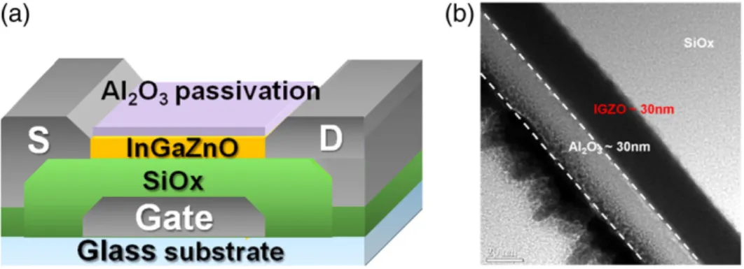
The bottom gate coplanar a-IGZO TFTs were produced on glass sub-strate in this study, and the fabrication details were described elsewhere
[16]. The schematic cross-section view and of the TFTs is shown in
Fig. 1(a). Briefly, the shaped Ti/Al/Ti (50/200/50 nm) gate electrodes were capped with 300-nm-thick SiOxgate dielectric. The source/drain
electrodes were formed with DC-sputtered Ti/Al/Ti (50/200/50 nm) and then patterned into the dimension of channel width/length (W/L)= 10–15 μm/9 μm by wet-etching. A 30-nm-thick a-IGZO thin film was de-posited as active layer by DC magnetron sputtering system using a target of In:Ga:Zn=1:1:1 in atomic ratio. After defining the active region by conventional photolithography, the devices were annealed in an oven at 330 °C for 2 h. Finally, the passivated device was capped with 30 nm thick Al2O3film by RF sputtering at room temperature, and annealed
again at 330 °C for 2 h to reduce the ion bombardment effect during the sputtering process [17]. The TFTs without any passivation were ⁎ Corresponding author at: Department of Physics, National Sun Yat-Sen University,
Kaohsiung, 804, Taiwan, ROC. Tel.: + 886 7 5252000 3708; fax: + 886 7 5253709. E-mail address:[email protected](T.-C. Chang).
0257-8972/$– see front matter. Crown Copyright © 2012 Published by Elsevier B.V. All rights reserved. doi:10.1016/j.surfcoat.2011.12.047
taken as reference devices for comparison.Fig. 1(b) also shows the cross-sectional transmission electron microscopy (TEM) image of the TFT de-vice. The laminated structure of the Al2O3/IGZO/SiOxin the TEM image
can easily be observed. The IGZOfilm is uniform without any observable microstructure, indicating that the IGZO layer is amorphous in structure although it was heated up to 330 °C during annealing. The electrical char-acteristics of the TFTs were analyzed by using Agilent B1500 system in the dark environment and measured in a vacuum chamber, a pressure of 10−3Torr to avoid the disturbance from atmosphere. The linear mobility was extracted by normal method of the square root normalized drain cur-rent (NID=ID×L/W) verse gate voltage (VG) plot, and the threshold
volt-age (Vth) is defined as the VGof the NIDreaching 1 nA. The sub-threshold
slope (SS) was extracted from NIDin the sub-threshold region (the NID
from 1−10A to 10−8A) under linear operation.
3. Results and discussion
Fig. 2(a) and (b) shows the transfer characteristics of the a-IGZO TFT for the unpassivated (device A) and passivated (device B) device during negative bias stress in dark (NBS), respectively. For the stress condition, the gate voltage wasfixed at the VGof−30 V and the S/D
electrodes were grounded. In the initial electrical properties, the device A exhibits the SS= 0.17 V/dec,field-effect mobility (u)=11.65 cm2/Vs,
and Vth=−0.6 V. The device B also shows excellent electrical
proper-ties, such as the SS = 0.34 V/dec,field-effect mobility (u)=11.14 cm2
/ Vs, and Vth=−1.3 V. Both of the devices with similar Ion/offratios of
108are observed. It indicates that a-IGZOfilm is not degraded during
the passivation Al2O3layer deposition by sputtering. In addition, both
of the devices show superior stabilities, without degradation of SS, on current, and obvious Vthshift during NBS.
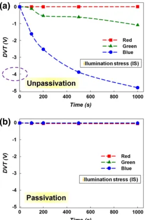
In order to study the instability under light illumination and dis-cuss the illuminated mechanism for devices with and without an Al2O3passivation layer, the devices expose in different wavelength
illumination were investigated.Fig. 3shows the spectra of LEDs, includ-ing red (photo-energy 1.93 eV), green (photo-energy 2.35 eV), and blue (photo-energy 2.64 eV) lights. All employed light sources in this study possess a sub-bandgap (a-IGZO).Fig. 4(a) and (b) show the correspond-ing Vthvariations of device A and B in the ID–VGcurves, respectively,
which are subjected to various colored illumination stresses (IS) without applying bias. The IS conditions are VG= VD= Vs = 0 V, and the light
in-tensity under illumination is 8000 lx for 1000 s. In device A, blue and green lights have negative threshold voltage shifts smaller than 5 V, but the electrical properties are stable in the red light illumination. Com-pared with device A, device B is stable in all the wavelength light illumi-nation, which slight threshold voltage shift is smaller than 0.5 V. The obvious Vthvariations of device A during the blue and the green IS can
be attributed to the O2desorption in the back channel of a-IGZO bulk.
Fig. 5(a) and (b) exhibits the schematic mechanisms for the proposed Fig. 1. (a) The cross-section schematic view of the fabricated a-IGZO TFT structure. (b) The cross-sectional TEM imaged of the a-IGZO thinfilm.
Fig. 2. Transfer characteristics for the (a) unpassivated (device A) and (b) passivatied
O2desorption model under light illumination for devices A and B,
re-spectively. Since the O2adsorbed on the a-IGZOfilm, which can capture
electrons in the back channel exists as O2−in a form of O2+ e−→O2−,
leading to a decrease of the carrier concentration of a-IGZOfilm and an increase in Vth [14,15,18,19]. However, under light illumination, the
holes generated from light inducing electron–hole pairs react with the absorbed O2−to reduce into O2in the back channel, resulting in a
nega-tive Vthshift. In addition, the blue light IS shows a larger negative Vth
shift than other wavelength lights (red and green), because the high
D–VG
istics of device A during negative bias red (photo-energy is 1.93 eV) illumination stress. Device A exhibits only a slight negative Vthshift
without other degradation during negative bias red light illumination stress (NBRIS). During the negative bias green light (photo-energy is 2.35 eV) illumination stress (NBGIS), a large negative Vthshift more
than NBRIS is present, as shown inFig. 6(b). Compared with NBRIS and NBGIS, device A exhibits a significant large photo leakage current during the negative bias blue light (photo-energy is 2.64 eV) illumina-tion stress (NBBIS), which induces a larger negative Vthshift more
than 15 V and a poor gate control on the channel current, as shown in
Fig. 6(c). This result indicates that the tendency of Vthshift increases
gradually as the light photo-energy increases during NBIS for device A. In contrast to device A, the I–V characteristics of device B during NBIS in different wavelength lights (red, green, and blue) show a superior stability, which the Vthslightly shifts (ΔVthb4 V) toward negative
direc-tion without degradadirec-tion of SS. The Vthshift also increases gradually as
the light photo-energy increases during NBIS.
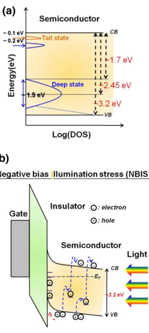
Fig. 7(a) shows the schematic models of subgap DOS in a-IGZO. The high density of occupied subgap states near the valence band with an en-ergy width of ~1.5 eV as reported by Nomura et al.[20,21].Fig. 7(b) ex-hibits the energy band of the a-IGZO TFT under NBIS. The subgap photon excitation can occur from the deep-subgap DOS to the conduction band under illumination when illumination light provides enough photo-energy (>1.7 eV), resulting in free electron concentration increases in the a-IGZOfilm[22]. Moreover, a negative bias is applied with illumination, resulting in the hole trapping in the insulator or a-IGZO/insulator inter-face[23,24]. Both of the results induce the apparent Vth shift under
NBIS. The short wavelength of illumination light has more photo-energy than long wavelength, which induces more free electron concentration and hole trapping. This result exhibits that the Vthshift also increases
gradually as the light photo-energy increases during NBIS. Compared to NBIS, the devices (devices A and B) show a superior stability without Vthshift during NBS. The lack of apparent Vthvariation under NBS can
Fig. 4. The light illuminated time dependence of Vthshift during various colored
illumina-tion stress (IS) without applying bias for (a) unpassivaillumina-tion (device A) and (b) passivated (device B) device.
be attributed to the negligible holes in the n-type ZnO-based material
[25,26]. Therefore, the hole trapping at either the gate insulator or at the a-IGZO interface can be ignored. However, the Al2O3passivation device
(device B) shows a slighter Vthshift (ΔVthb4 V) than the device A during
NBIS, because the Al2O3passivation layer decreases the deep-subgap
den-sity that induces the photo-excitation behavior decrease. Hence, the Al2O3
is an effective passivation layer to suppress the photo-excitation on a-IGZO film that enhances the illumination stability and negative bias light illumination stability.
4. Conclusion
In conclusion, the Al2O3passivation layer enhancing the
illumina-tion stable was investigated. The Al2O3passivation layer suppresses
the gas adsorption/desorption in the back channel of a-IGZOfilm. It in-duces the electrical property that shows a more stability (ΔVthb0.5 V)
during all wavelength lights IS. In contrast, no passivation device shows a larger negative Vthshift than Al2O3passivation device because
the holes generated form light inducing electron–hole pairs react with Fig. 6. Transfer I–V characteristics for the unpassivation (device A) during the negative bias illumination stress (NBIS) of (a) red, (b) green, and (c) blue lights. Transfer I–V char-acteristics for the passivation (device B) during the negative bias illumination stress (NBIS) of (d) red, (e) green, and (f) blue lights.
the absorbed O2−to reduce into O2under illumination. Otherwise, the
negative bias illumination stress induced instability of the electrical properties was investigated in the study. The subgap photon excitation occurs from the deep-subgap DOS inducing that the hole generates and traps in the insulator or IGZO/insulator interface under NBIS, resulting in the apparent negative Vthshift. However, the Al2O3passivation
de-vice exhibits a slighter Vthnegative shift (ΔVthb4 V) than the no
pas-sivation device under NBIS due to the decrease of hole trapping. The hole trap decreases because the Al2O3passivation layer decreases
the deep-subgap density that results in the photo-excitation behav-ior decrease. In addition, Hence, Al2O3 is an effective passivation
layer to suppress gas absorption on InGaZnO back channel and de-crease photo-excitation behavior.
Dig. (1998) 871.
[2] R.M.A. Dawson, Z. Shen, D.A. Furest, S. Connor, J. Hsu, M.G. Kane, R.G. Stewart, A. Ipri, C.N. King, P.J. Green, R.T. Flegal, S. Pearson, C.W. Tang, S. Van Slyke, F. Chen, J. Shi, M.H. Lu, J.C. Sturm, IEDM Tech. Dig. (1998) 875.
[3] H.Y. Lu, P.T. Liu, T.C. Chang, S. Chi, IEEE Electron Device Lett. 27 (2006) 743. [4] T.C. Chen, T.C. Chang, T.Y. Hsieh, W.S. Lu, F.Y. Jian, C.T. Tsai, S.Y. Huang, C.S. Lin,
Appl. Phys. Lett. 99 (2011) 022104.
[5] J.S. Park, T.W. Kim, D. Stryakhilev, J.S. Lee, S.G. An, Y.S. Pyo, D.B. Lee, Y.G. Mo, D.U. Jin, H.K. Chung, Appl. Phys. Lett. 95 (2009) 013503.
[6] Y.C. Chen, T.C. Chang, H.W. Li, S.C. Chen, J. Lu, W.F. Chung, Y.H. Tai, T.Y. Tseng, Appl. Phys. Lett. 96 (2010) 262104.
[7] C.T. Tsai, T.C. Chang, S.C. Chen, I. Lo, S.W. Tsao, M.C. Hung, J.J. Chang, C.Y. Wu, C.Y. Huang, Appl. Phys. Lett. 96 (2010) 242105.
[8] H. Kumomi, K. Nomura, T. Kamiya, H. Hosono, Thin Solid Films 516 (2008) 1516. [9] W.F. Chung, T.C. Chang, H.W. Li, S.C. Chen, Y.C. Chen, T.Y. Tseng, Y.H. Tai, Electrochem.
Solid-State Lett. 14 (6) (2011) H235.
[10] M.C. Chen, T.C. Chang, S.Y. Huang, K.C. Chang, H.W. Li, S.C. Chen, J. Lu, Y. Shi, Appl. Phys. Lett. 94 (2009) 162111.
[11] K.H. Ji, J.-I. Kim, Y.-G. Mo, J.H. Jeong, S. Yang, C.-S. Hwang, S.-H.K. Park, M.-K. Ryu, S.-Y. Lee, J.K. Jeong, IEEE Electron Device Lett. 31 (2010) 1404.
[12] M.C. Chen, T.C. Chang, S.Y. Huang, S.C. Chen, C.W. Hu, C.T. Tsai, Simon M. Sze, Electrochem. Solid-State Lett. 13 (6) (2010) H191.
[13] M.C. Chen, T.C. Chang, C.T. Tsai, S.Y. Huang, S.C. Chen, C.W. Hu, S.M. Sze, M.J. Tsai, Appl. Phys. Lett. 96 (2010) 262110.
[14] D. Kang, H. Lim, C. Kim, I. Song, J. Park, Y. Park, J.G. Chung, Appl. Phys. Lett. 90 (2007) 192101.
[15] J.S. Park, J.K. Jeong, H.J. Chung, Y.G. Mo, H.D. Kim, Appl. Phys. Lett. 92 (2008) 072104.
[16] S.Y. Huang, T.C. Chang, M.C. Chen, S.C. Chen, C.T. Tsai, M.C. Hung, C.H. Tu, C.H. Chen, J.J. Chang, W.L. Liau, Electrochem. Solid-State Lett. 14 (4) (2011) H177. [17] J. Park, S. Kim, C. Kim, S. Kim, I. Song, H. Yin, K.-K. Kim, S. Lee, K. Hong, J. Lee, J.
Jung, E. Lee, K.-W. Kwon, Y. Park, Appl. Phys. Lett. 93 (2008) 053505. [18] J.K. Jeong, H.W. Yang, J.H. Jeong, Y.G. Mo, H.D. Kim, Appl. Phys. Lett. 93 (2008)
123508.
[19] T.C. Chen, T.C. Chang, T.Y. Hsieh, C.T. Tsai, S.C. Chen, C.S. Lin, M.C. Hung, C.H. Tu, J.J. Chang, P.L. Chen, Appl. Phys. Lett. 97 (2010) 192103.
[20] K. Nomura, T. Kamiya, H. Yanagi, E. Ikenaga, K. Yang, K. Kobayashi, M. Hirano, Hosono, Appl. Phys. Lett. 92 (2008) 202117.
[21] H. Oh, S. Mi . Yoon, M.K. Ryu, C.S. Hwang, S. Yang, S.H.K. Park, Appl. Phys. Lett. 97 (2010) 183502.
[22] K.-H. Lee, J.S. Jung, K.S. Son, J.S. Park, T.S. Kim, R. Choi, J.K. Jeong, J.-Y. Kwon, B. Koo, S. Lee, Appl. Phys. Lett. 95 (2009) 232106.
[23] P. Görrn, M. Lehnhardt, T. Riedl, W. Kowalsky, Appl. Phys. Lett. 91 (2007) 193504. [24] J.H. Shin, J.S. Lee, C.S. Hwang, S.H.K. Park, W.S. Cheong, M. Ryu, C.W. Byun, J.I. Lee,
H.Y. Chu, ETRI J. 31 (2009) 62.
[25] A. Suresh, J.F. Muth, Appl. Phys. Lett. 92 (2008) 033502.
[26] M.E. Lopes, H.L. Gomes, M.C.R. Medeiros, P. Barquinha, L. Pereira, E. Fortunato, R. Martins, I. Ferreira, Appl. Phys. Lett. 95 (2009) 063502.
Fig. 7. (a) Schematic model of subgap DOS in a-IGZO TFTs. (b) Energy band diagram of explain the negative bias illumination stress instability.