Enhancing luminescence efficiency of InAs quantum dots at 1.5 m using a carrier
blocking layer
Tung-Po Hsieh, Pei-Chin Chiu, Jen-Inn Chyi, Hsiang-Szu Chang, Wen-Yen Chen, Tzu Min Hsu, and Wen-Hao Chang
Citation: Applied Physics Letters 89, 053110 (2006); doi: 10.1063/1.2245374 View online: http://dx.doi.org/10.1063/1.2245374
View Table of Contents: http://scitation.aip.org/content/aip/journal/apl/89/5?ver=pdfcov Published by the AIP Publishing
Articles you may be interested in
Gain dynamics of an InAs/InGaAsP quantum dot semiconductor optical amplifier operating at 1.5 m Appl. Phys. Lett. 98, 011107 (2011); 10.1063/1.3533365
Polarization control of gain of stacked In As In P (100) quantum dots at 1.55 m : Interplay between ground and excited state transitions
Appl. Phys. Lett. 92, 123113 (2008); 10.1063/1.2904703
Design, growth, fabrication, and characterization of In As Ga As 1.3 m quantum dot broadband superluminescent light emitting diode
J. Appl. Phys. 100, 103105 (2006); 10.1063/1.2365387
Saturable absorption of highly stacked InAs quantum dot layer in 1.5 m band Appl. Phys. Lett. 89, 151117 (2006); 10.1063/1.2357598
Quantum dot strain engineering for light emission at 1.3, 1.4 and 1.5 m Appl. Phys. Lett. 87, 063101 (2005); 10.1063/1.2007860
This article is copyrighted as indicated in the article. Reuse of AIP content is subject to the terms at: http://scitation.aip.org/termsconditions. Downloaded to IP: 140.113.38.11 On: Thu, 01 May 2014 01:54:08
Enhancing luminescence efficiency of InAs quantum dots
at 1.5
m using a carrier blocking layer
Tung-Po Hsieh, Pei-Chin Chiu, and Jen-Inn Chyia兲
Department of Electrical Engineering, National Central University, Jhongli, 32001 Taiwan,
Republic of China and Optical Sciences Center, National Central University, Jhongli, 32001 Taiwan, Republic of China
Hsiang-Szu Chang, Wen-Yen Chen, and Tzu Min Hsu
Department of Physics, National Central University, Jhongli, 32001 Taiwan, Republic of China and Center for Nano Science and Technology, National Central University, Jhongli, 32001 Taiwan, Republic of China
Wen-Hao Chang
Institute of Electrophysics, National Chiao-Tung University, Hsinchu, 300 Taiwan, Republic of China and Department of Electrophysics, National Chiao-Tung University, Hsinchu, 300 Taiwan,
Republic of China
共Received 8 March 2006; accepted 13 June 2006; published online 1 August 2006兲
The authors report an effective way to enhance the optical efficiency of InAs quantum dots共QDs兲 on GaAs emitting at the wavelength of 1.5m. It is found that the loss of holes from QDs to their proximity via the high indium composition InGaAs overgrown layer, which is necessary for achieving long wavelength emission, is the origin of photoluminescence intensity degradation at high temperature. Inserting a 4 nm thick Al0.45Ga0.55As layer, acting as a carrier blocking layer, into the GaAs capping matrix can improve the room temperature photoluminescence peak intensity by five and two times for the ground and first excited states, respectively. © 2006 American Institute of Physics. 关DOI:10.1063/1.2245374兴
With the advantages of mature material technology over InP and low dimensional quantum effect, InAs quantum dot 共QD兲 lasers on GaAs substrate emitting at 1.3 or 1.55m have been actively pursued for ligthwave communications. In the past few years, much progress has been made on 1.3m QD lasers based on self-assembled InAs/ GaAs QDs grown by molecular beam epitaxy, in terms of threshold current,1 modulation speed,2,3 linewidth enhancement factor,3,4characteristic temperature,3,5and differential quan-tum efficiency.6 However, the work on 1.5m range QD lasers has not been so successful due to the rapid deteriora-tion in structural and optical properties of the high indium containing heterostructure unless a metamorphic buffer layer is used.7There are also several groups trying to achieve the same target using metal-organic chemical vapor deposition 共MOCVD兲, which is considered a better technique for mass production. So far, there are only two groups that have been able to extend the emission wavelength of InAs QDs on GaAs to 1.5m regime using MOCVD.8,9However, the lu-minescence efficiency of the QDs still decreases significantly as the emission wavelength is extended to 1.5m by cap-ping the QDs with a high indium composition InGaAs layer. It hampers the realization of 1.55m QD lasers on GaAs.
Previously, we have demonstrated that the luminescence efficiency of long wavelength InAs QDs can be improved by using triethylgalliun precursor for the growth of the GaAs cap layer.9 In the present study, we find an effective way to further improve the luminescence efficiency of InAs QDs. A wide band gap material, which acts as a carrier blocking layer共CBL兲, is inserted into the GaAs matrix to effectively alleviate photoluminescence共PL兲 quenching of InAs QDs.
The samples were grown by low-pressure MOCVD in a vertical reactor. The precursors are trimethylindium 共TMI兲, trimethylgallium共TMG兲, triethylgallium 共TEGa兲, trimethyla-luminium 共TMAl兲, and arsine 共AsH3兲. We prepared two
types共types I and II兲 of samples in this study. The schematic drawings of type-I and type-II samples are shown in Figs. 1共a兲 and 1共b兲, respectively. Type-I samples are designed to
a兲Electronic mail: [email protected] FIG. 1. Schematic of InAs QDs embedded in GaAs matrix共b兲 with carrier blocking layer. 共a兲 without and APPLIED PHYSICS LETTERS 89, 053110共2006兲
0003-6951/2006/89共5兲/053110/3/$23.00 89, 053110-1 © 2006 American Institute of Physics
This article is copyrighted as indicated in the article. Reuse of AIP content is subject to the terms at: http://scitation.aip.org/termsconditions. Downloaded to IP: 140.113.38.11 On: Thu, 01 May 2014 01:54:08
extend the emission wavelength of InAs QDs by a single overgrown layer while the second set of samples 共type II兲 contains an additional CBL in the GaAs cap matrix for the enhancement of luminescence efficiency of QDs. Before the growth of the InAs QDs, a 0.2m thick GaAs buffer layer was grown on 共100兲 2° off towards 共111兲A Si-doped n + GaAs substrate at 650 ° C using TMGa and AsH3 as the
source materials. The substrate temperature was then low-ered to 500 ° C for the growth of QDs and all the layers above the dots. Self-assembled InAs QDs were grown by depositing 2.7 ML of InAs with a deposition rate of 0.1 ML/ s. From atomic force microscopy measurements on separate samples, these growth parameters led to QDs of about 20 nm in diameter, 6 nm in height, and a typical dot density of about 2⫻1010 cm−2. The InAs QDs were then
embedded in a 9 nm thick InGaAs overgrown layer using TMGa, TMI, and AsH3 as the source materials. For tuning the emission wavelength of QDs, indium composition of the InGaAs overgrown layer was varied from 0% to 31%. Samples were finally capped with an 80 nm thick GaAs grown using TEGa and AsH3. For the type-II samples, a
4 nm thick Al0.45Ga0.55As layer, grown by TMAl, TMGa, and AsH3, was inserted into the GaAs cap matrix, as shown
in Fig. 1共b兲. The PL measurements were carried out between 10 and 300 K using the 514.5 nm line of an Ar ion laser as the excitation source.
Figure 2共a兲 shows the room temperature PL spectra of type-I samples. Here, the overgrown layer is InxGa1−xAs with
indium composition x = 0, 0.17, 0.23, and 0.31, respectively. The QDs with a pure GaAs overgrown layer关solid line in Fig. 2共a兲兴 exhibited two PL peaks at 1.31 and 1.22m, which correspond to the ground state and the first excited state transitions, respectively. For the QDs with an InGaAs overgrown layer, the PL wavelength shifts to longer wave-length with increasing indium composition of the InGaAs overgrown layer. Emission wavelength for the ground state transition as long as 1.55m is obtained for the QDs with an In0.31Ga0.69As overgrown layer. There are two mechanisms
proposed to account for the redshift of the QD emission by an overgrown layer. One is the relaxation of compressive hydrostatic strain in QDs共Refs. 10 and 11兲 and the other is the increased volume of QDs caused by phase separation of the InGaAs overgrown layer.12–14Concurrently, the PL inten-sity of QDs decreases seriously as the indium composition of the overgrown layer is increased. According to previous works,8,9 the degradation of PL intensity of QDs with high indium composition InGaAs overgrown layer is attributed to two defect-related reasons. One is the increased nonradiative recombination centers within the high indium composition InGaAs layer.8 The other is proposed by the authors that nonradiative recombination centers in the GaAs cap layer also play a role in PL quenching because the resultant large
QDs make smooth coverage of QDs by the GaAs cap layer difficult.9 Although we have used triethylgalliun precursor for the growth of the GaAs cap layer to improve their optical property in 1.55m range, the PL intensity of the QDs decreases still to about one-thirtieth as the indium composi-tion of the overgrown layer is increased from 0% to 31% and their activation energy deduced from the
temperature-dependent integrated PL intensity decreases from
133 to 87 meV as well. These values are comparable to the energy difference between the hole first excited states in QD and the valence bands of GaAs 共⬃134 meV兲 and InGaAs 共⬃89 meV兲 as illustrated in Figs. 2共b兲 and 2共c兲, respectively. This is in good agreement with our previous studies on
car-rier escape mechanisms using PL and photocurrent
techniques.15,16 It is therefore speculated that the high indium-content InGaAs overgrown layer, which is used to extend the emission wavelength of QDs, provides an easy path for holes to thermally escape from QDs.
To clarify this point, type-II samples were prepared, con-taining a 4 nm thick Al0.45Ga0.55As layer named as CBL as
will be explained later. Figure 3共a兲 shows the PL spectra of two samples emitting at 1.5m with 共type II兲 and without 共type I兲 CBL at room temperature. In both samples, the in-dium composition of the InGaAs overgrown layer was 30%. By introducing the CBL, the PL intensity increased about five times for the ground state peak and two times for the first excited state peak. A possible reason for this is that carriers could be confined in the QD structure due to the CBL as indicated by the blueshift 共⬃6 meV兲 in emission wavelength. However, the improved quantum confinement along cannot account for such a significant enhancement in luminescence efficiency, especially when the CBL is not di-rectly in contact with QDs.17It is illustrative to compare the present case with the reported ones, which employ wide band gap overgrown layers, such as Al共Ga兲As 共Ref. 18兲 and InAlAs.19–21 In those cases, the energy difference between the ground state and the excited state emission is increased by about 10– 40 meV as compared to the case where an In-GaAs cap layer is deposited, like in our type-I sample. How-ever, our type-II sample shows an increase of only 6 meV, indicating that the AlGaAs CBL does not increase quantum confinement as much as wide band gap overgrown layers do. For more insight into the PL improvement mechanism of InAs QDs with an AlGaAs CBL, the temperature depen-dence of the integrated intensity of both types of QD samples 共types I and II兲 was examined. Figure 3共b兲 shows the Arrhen-ius plot of integrated PL intensity of type-I and type-II samples between 20 and 300 K. The type-I sample shows a typical behavior of thermally activated nonradiative
recom-FIG. 2.共a兲 PL spectra of QDs with an InGaAs overgrown layer of various indium compositions and the band diagram for the InAs QDs共b兲 without
and共c兲 with an InGaAs overgrown layer. FIG. 3.共a兲 PL spectra of QDs embedded in GaAs matrix with and without CBL at 300 K, and共b兲 temperature dependence of the integrated PL inten-sity of QDs embedded in GaAs matrix with and without a carrier blocking layer.
053110-2 Hsieh et al. Appl. Phys. Lett. 89, 053110共2006兲
This article is copyrighted as indicated in the article. Reuse of AIP content is subject to the terms at: http://scitation.aip.org/termsconditions. Downloaded to IP: 140.113.38.11 On: Thu, 01 May 2014 01:54:08
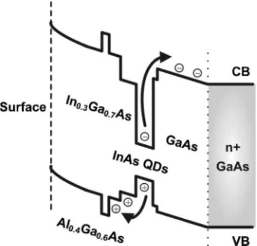
bination of QDs. Its integrated PL intensity quenches slowly as the temperature increases from 20 to 130 K and then rap-idly from 130 to 300 K. This behavior is usually attributed to thermally enhanced carrier recombination in nonradiative centers located at the vicinity of the QDs,22or carrier escape and then recombination in the wetting layer and/or GaAs matrix.15 The type-II sample, on the other hand, shows a more extended high intensity range. Its activation energy is estimated to be 155 meV as compared to 87 meV for the type-I sample. Though the increase of activation energy is not as high as the energy barriers introduced by the AlGaAs CBL for holes, this value is still higher than the case with only a GaAs overgrown layer. The lower than expected ac-tivation energy might be attributed to hole tunneling that enhanced by the built-in field due to surface band bending. This process can be depicted by Fig. 4, which is the sche-matic band diagram of the type-II sample. The holes that blocked by this barrier may create a retarded field to prevent further escape of holes from the QDs or even enhance the retrapping process,23as implied by the slight increase in PL intensity when the temperature increases from 130 to 140 K. Although this carrier blocking and retrapping effect becomes less pronounced above 140 K due to the increased thermal energy of holes, the overall PL intensity of the type-II sample is still much higher than that of its type-I counterpart.
In summary, we have shown that the optical efficiency of InAs QDs emitting at 1.5m grown on GaAs can be im-proved with the presence of a high band gap material acting as a carrier blocking layer. Our results indicate that the loss of holes via high indium composition InGaAs overgrown layer is responsible for the PL degradation of InAs QDs emitting at 1.5m range. By inserting an AlGaAs layer in the GaAs matrix, the PL intensity is effectively enhanced as a result of holes blocking and retrapping process. High lumi-nescence efficiency InAs QDs on GaAs emitting at 1.5m
can thus be prepared without complicated metamorphic buffer growth.
This work was partially supported by the National Sci-ence Council of Taiwan, under Contract Nos. 94-2215-E-008-004, 94-2752-E-008-001-PAE, and 93-2120-M-008-001, and the Center for Nano Science and Technology of the University System of Taiwan.
1H. Y. Liu, D. T. Childs, T. J. Badcock, K. M. Groom, I. R. Sellers, M.
Hopkinson, R. A. Hogg, D. J. Robbins, D. J. Mowbray, and M. S. Skolnick, IEEE Photonics Technol. Lett. 17, 1041共2005兲.
2S. M. Kim, Y. Wang, M. Keever, and J. S. Harris, IEEE Photonics
Tech-nol. Lett. 16, 377共2004兲.
3Z. Mi, P. Bhattacharya, and S. Fathpour, Appl. Phys. Lett. 86, 153109
共2005兲.
4A. Martinez, A. Lemaitre, K. Merghem, L. Ferlazzo, C. Dupuis, A.
Ramdane, J.-G. Provost, B. Dagens, O. Le Gouezigou, and O. Gauthier-Lafaye, Appl. Phys. Lett. 86, 21115共2005兲.
5S. Fathpour, Z. Mi, S. Chakrabarti, P. Bhattacharya, A. R. Kovsh, S. S.
Mikhrin, I. L. Krestnikov, A. V. Kozhukhov, and N. N. Ledentsov, Appl. Phys. Lett. 85, 5164共2004兲.
6A. R. Kovsh, N. A. Maleev, A. E. Zhukov, S. S. Mikhrin, A. R. Vasilev,
Yu. M. Shernyakov, M. V. Maximov, D. A. Livshits, V. Ustinov, Zh. I. Alferov, N. N. Ledentsov, and D. Bimberg, Electron. Lett. 38, 1104 共2002兲.
7N. N. Ledentsov, A. R. Kovsh, A. E. Zhukov, N. A. Maleev, S. S.
Mikhrin, A. P. Vasil’ev, E. S. Semenova, M. V. Maximov, Yu. M. Shernyakov, N. V. Kryzhanovskaya, V. M. Ustinov, and D. Bimberg, Electron. Lett. 39, 1126共2003兲.
8J. Tatebayashi, M. Nishioka, and Y. Arakawa, Appl. Phys. Lett. 78, 3469
共2001兲.
9T. P. Hsieh, N. T. Yeh, P. C. Chiu, W. H. Chang, T. M. Hsu, W. J. Ho, and
J.-I. Chyi, Appl. Phys. Lett. 87, 151903共2005兲.
10K. Nishi, H. Saito, S. Sugou, and J.-S. Lee, Appl. Phys. Lett. 74, 1111
共1999兲.
11N. T. Yeh, T. E. Nee, J.-I. Chyi, C. C. Huang, and T. M. Hsu, Appl. Phys.
Lett. 76, 1567共2000兲.
12M. V. Maximov, A. F. Tsatsul’nikov, B. V. Volovik, D. S. Sizov, Y. M.
Shernyakov, I. N. Kaiander, A. E. Zhukov, A. R. Kovsh, S. S. Mikhrin, V. M. Ustinov, Z. I. Alferov, R. Heitz, V. A. Shchukin, N. N. Ledentsov, D. Bimberg, Y. G. Musikhin, and W. Neumann, Phys. Rev. B 62, 16671 共2000兲.
13F. Guffarth, R. Heitz, A. Schliwa, O. Stier, N. N. Ledentsov, A. R. Kovsh,
V. M. Ustinov, and D. Bimberg, Phys. Rev. B 64, 085305共2000兲.
14W. H. Chang, H. Y. Chen, H. S. Chang, W. Y. Chen, T. M. Hsu, T. P.
Hsieh, J.-I. Chyi, and N. T. Yeh, Appl. Phys. Lett. 86, 131917共2005兲.
15W. H. Chang, T. M. Hsu, C. C. Huang, S. L. Hsu, C. Y. Lai, N. T. Yeh, and
J.-I. Chyi, Phys. Rev. B 62, 6959共2000兲.
16W. H. Chang, W. Y. Chen, T. M. Hsu, N. T. Yeh, and J.-I. Chyi, Phys. Rev.
B 66, 195337共2002兲.
17J. L. Movilla, J. I. Climente, and J. Planelles, J. Appl. Phys. 94, 4515
共2003兲.
18M. Arzberger, U. Käsberg, G. Bohm, and G. Abstreiter, Appl. Phys. Lett.
75, 3968共2002兲.
19W.-S. Liu and J.-I. Chyi, J. Appl. Phys. 97, 024312共2005兲. 20H. Y. Liu and M. Hopkinson, Appl. Phys. Lett. 82, 3644共2003兲. 21Y. Q. Wei, S. M. Wang, F. Ferdos, J. Vukusic, and A. Larsson, Appl. Phys.
Lett. 81, 1621共2002兲.
22E. C. Le Ru, P. D. Siverns, and R. Murray, Appl. Phys. Lett. 77, 2446
共2000兲.
23G. Saint-Girons and I. Sagnes, J. Appl. Phys. 91, 10115共2002兲.
FIG. 4. Carrier escape processes of InAs QDs embedded in GaAs matrix with a carrier blocking layer.
053110-3 Hsieh et al. Appl. Phys. Lett. 89, 053110共2006兲
This article is copyrighted as indicated in the article. Reuse of AIP content is subject to the terms at: http://scitation.aip.org/termsconditions. Downloaded to IP: 140.113.38.11 On: Thu, 01 May 2014 01:54:08