ELSEVIER Materials Chemistry and Physics 52 ( 1998) 17-22
MATERIALS
CHEMJ;\‘NW&lD
The exothermic reaction and temperature measurement for tungsten CMP
technology and its application on endpoint detection
Y.-L. Wang ‘**, C. Liu b, M.-S. Feng b, W.-T. Tseng ’
’ lmrimre ofE/ecrrork-s, N&orzai Chino-Twzg &ivelsiry, Hsinch~, T&WI, ROC
’ lmrirure of M~~r~riois Scicncc cd Engkering, Nnfionai ChicwTwzg Universi@, Hsinciz~, Tuirran, ROC ’ Nnrio~w~l Nnno Det?ce Laborcuoy, Hsinchu, Tninm, ROC
Received 19 March 1997: received in revised form 9 May 1997: accepted 3 June 1997
- Abstract
A novel in-situ endpoint detection method used pad temperature measurement to control the polishing tungsten and barrier metal Ti/TiN is proposed. The metal chemical-mrchanical polishing (CMP) process includes chemical reaction. It is an exothermic process as the polishing slurry reacts on tungsten and Ti/TiN films. Therefore. the pad temperature increases as tungsten and barrier metal films are polished, but will drop dramatically when metal layers are polished and touch the oxide layer. A non-contact thermal sensor system was installed on our CMP tool to measure the pad tcmperarure. From rhe in-situ pad temperature curve, the endpoint can be detected clearly and the polishing process stops at the oxide layer. This method can also be used to study the reactions between the pad temperature curve and the effects of CMP process conditions such as down force, platen speed as well as polishing performance such as removal rate and uniformity. 0 1998 Elsevier Science S.A.
Ke~ito&: Chemical-mechanical polishing: Endpoint detection; Tungsten plu g; Tungsten CMP: Pad temperature
1. Introduction
The application of tungsten chemical-mechanical polish- ing (CMP) technology for ULSI manufacturing has become indispensable as the design rule approaches the quarter micron era. CMP is believed to be the only technology of choice for the global planarization of dielectric and formation of metal plugs and interconnects [ l-31. Polishing of the tungsten (W) plug structure is more controllable and results in a higher yield than current etch back process [ 41. In the W-CMP process, it is very important to achieve low defect, low oxide erosion and superior final plug morphology [ 4.51. Blanket tungsten is generally deposited the uses the CVD techniques for the W-plug structure. Also, titanium (Ti) and titanium nitride (TiN) is commonly used as the under layer for W-CVD. The Ti/TiN/W stack-film structure is a typical process flow. Tungsten polish endpoint is usually imple- mented by time-mode for different films polishing rate mon- itoring. This is not a competitive way for mass production to meet deposition and polishing machine variations. Further-
* Corresponding author. Taiwan Semiconductor Manufacturing Co. Ltd.. No. 9 Creation Rd. I. Science-Based Industrial Park. Hsin-Chu, Taiwan. ROC.
02540581/98/$19.00 0 1998 Elwvier Science S.A. All rights reserved PllSO254-Oj84(97)01990-2
more, the polishing rates for Ti, TiN, and W are quite differ- ent. The polishing rate depends not only on the material properties of pad, the film itself, the area in contact with pad, applied pressure, platen and spindle speeds of tool, but also on the pad lifetime cycle. It is quite difficult to determine the time in which the polishing is completed and stops the proc- ess. Therefore, a precise endpoint detection technique is needed. In the past, numerous improvements to the endpoint detection for oxide CMP have been invented, such as acous- tical waves method [ 61, motor current technique [7], di- electric capacitor characteristic measurement and optical method by impinging laser light [S]. However. the above approaches need to change the design system of platen/pad or induce extra signals into wafer which makes the detection system complex and expensive. They have only been tried in dielectric CMP and have not yet succeeded in applying on the W-plug pattern structure for the CMP process. A new endpoint detection method for measuring the pad temperature during the W-CMP process is studied in this paper. This method is simpler and less expensive than other methods. With the implementation of this method, the polishing para- meters such as down force, platen speed and the change of film properties and uniformity to optimize the W-CMP proc- ess are also investigated.
18 Y.-L. Wung ef ul. /Matrritrls Chrrnisrtyc rind Physics 52 (199s) 17-22
2. Experiment
Wafers with 200 mm diameter are first coated on 1 pm PECVD SiOz film, then followed by the materials to be char- acterized. Wafers of 6000 A thick TiN or Ti films were depos- ited on blanket oxide substrate using an Applied Material Endura PVD system for the test study and also for determi- nation of removal rates. For the tungsten polishing study, 5900 w W / 100 w TiN films were stacked on oxide substrate in order to eliminate the peeling oftungsten film. The Applied Material Centura WCVD system was used for tungsten dep- osition. Test structures consisting of both contact features and inlaid features were used for the study of W-plug patterned wafers. The patterned wafers consisted of 5000 .& WI500 w TiN/SOO Ti film stack. The data were typically collected from W-plug area with 0.5 p,rn in plug size, 1 pm in plug depth, and 3 pm in pitch.
A Westech Model 472 chemical-mechanical planarizer
was used for polishing, post-polish buffing, and high pressure DI water spindle rinsing at high spindle rotation. Wafers were polished on the primary platen using a IC lOOO/Suba IV perforated pad from Rodel. Post-polish buffing was per- formed on the secondary platen using a high nap Polytex Supreme pad from Rodel. A typical polishing procedure is: down force, 5 psi; platen speed, 50 rpm; carrier speed, 50 rpm; back pressure, 0 psi and slurry Row rate,
125 ml min-‘. Three types of commercially available slur-
ries were used for this study. A summary of the basic char- acteristics of these slurries is shown in Table 1.
A non-contact thermal sensor system was installed on our CMP tool to measure the pad temperature. As shown in Fig.
1, the non-contact thermal sensor (M500 from Mikron Instru- ment Company, Inc.) was fixed on the polishing arm to mon- itor the pad temperature near the polished wafer. The output voltage signals from the thermal sensor were collected by computer through a DVM card. The output voltage of the sensor varies linearly with the temperature measured. This method can real-time record the whole history of the CMP process and thus provides valuable information through tern- perature reading. The metal film thickness and uniformity were obtained from the sheet resistance measured by a Tencor RS-75 four point probe system,
3. Results and discussion
The pad temperature profiles in the CMP process for blan- ket tungsten test wafers are shown in Fig. 1. It shows that the pad temperature increases first then drops during the CMP process. The reason for this phenomenon is that the metal CMP is a combination of chemical reaction and mechanical abrasion, In the W-CMP, slurries consist of a low pH value oxidizing agent huch as KIO, or Fe{ NO,), and the mechan- ical abrasive particles (typically Al,O,) . When the surface
of W-wafer is in contact with slurry, a passivation layer is formed on the tungsten surface. Eq. ( 1) shows the typical chemical reaction of tungsten in the acidic environment.
W + [Oxidizer] ’ + H+ --f WO, + [Oxidizer]’ (1)
This oxidation chemical reaction is usually an exothermic reaction and pad temperature increases during the W-CMP polishing process. The removal of the formed passivation layer by mechanical polishing is a frictional heating process
which enhances the increase of pad temperature. The polish- ing steps were repeated as the new passivation layer was
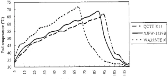
formed by chemically exothermic reaction. The passivation layer was then removed by mechanical frictional process until the polishing completed and stopped on the oxide layer. The temperature increased as the tungsten was polished and dropped immediately when polishing was complete, ready to commence on the oxide layer. Fig. 2 shows the typical pad temperature curves measured from a non-contact thermal sen- sor. Temperature drop indicates that the chemical oxidation reaction of the tungsten film stops as the tungsten film finishes polishing. The room temperature slurries removed the heat immediately. Similar experiments were also demonstrated for the TIN and Ti blanked test wafers. Figs. 3 and 4 show the pad temperature profile of polishing TiN and Ti films. The results show that the temperature profile curves is similar to the curve of the W-CMP process. Hence the polishing mech- anism of barrier metal films are similar to W-CMP which are exothermic oxidation reaction and mechanical frictional polishing.
Table 1
The basic characteristics of three type of W slurries
Slurry vender Rode1 Rode1 Cabot Slurry type QCTTlOll
pH at 25°C 4.3 Oxidation agent KIO; Abrasive materials AlzO,
75 / I i0
Fig. 2. The pad temperature profile during the blanket W wafers polishing for different slurries.
- - QCTTIOII- -xxJFN’-3,39B . . - WA35VFElO~ 30 25 I '.' I b- 2 2 F s : z F E 2 g " - -
P&h t,me (,econd)
Fig. 3. The pad temperature profile during the blanker TiN wafers polishing for different slurries.
75 70
Fig. 1. The pad temperature protile during the blanket Ti wafers polishing for different slurries.
In Figs. 2-4 it can be found that the temperature curves with using WA 355/FElO slurry to polish W, Ti and TiN films are higher than those of XJFW-3139B and QCTTlOl 1 slurries. The lower pH value of WA3SS/FElO accounts for this phenomenon. In Eq. ( 1 ). it can be seen that the lower pH value of slurry enhances the oxidation reaction on the metal films. Hence the higher removal rate and higher pad temperature during the polishing process can be expected. It can also be found that a relatively higher temperature curve occurs when polishing the TIN film and a relatively lower temperature curve occurs when polishing the Ti film. com- parison shown in Figs. 2-4. It is believed that the different removal rates of thebe films are related to this result. To examine this hypothesis, the removal rates of these three films with using the W-slurries have been checked by the RS-75 four point probe system. Thickness variations have been obtained for the first 30 or 60 s during the polishing process. Then the removal rates of thebe films were calculated. The
Table 2
The removal rates (A min-‘) of W. TIN, and Ti with different types of slurries Slurry W (Rs-751 TIN (Rs-75/ Temp. ) Temp.) Ti (Rs-751 Temp.) QCTTlOll 356113728 132814433 234112422 XJFW3 139B 388911006 453514728 2531/2598 WA355/FElO 4960/j 132 641316598 29831320 1
removal rates could also be calculated with the thickness change divided by the time difference at the peaks in Figs. 2-4.
Removal rate (;\ min- ’ ) = fil~~~~~~,ge (2) Table 2 shows the removal rates obtained from thebe two methods. They are consistent with each other, and the removal rate of TIN film is the relatively highest in these three films within one slurry. Therefore, higher polishing removal rate has been proven to result in higher pad temperature. The pad temperature curve could be used to sense the removal rate determination.
3.2. Pattern wafer test
The wafers which consisted of W 5000 AlTiN 500 P\ITi 500 A film stack on plug pattern were polished. Fig. 5 shows the pad temperature profile with these three types of slurries. The results showed that the temperature increased first and reached its maximum, then dropped immediately. It is thought that film interface change accounted for this temper- ature drop during the polishing process. That is, the polishing film changing from the metal film to the oxide causes the temperature trend change (drop) and it can be used as the endpoint signal for the process of polishing metal film. The conventional ways used to predict the endpoint of the polish- ing pattern stack structure such as W, Ti, and TiN are calcu- lated from the thickness of these films divided by the removal rates of these metal films on the blanket wafers. Table 3 shows the prediction time of endpoint of W, Ti, TIN from temper- ature curve in Fig. 5 and blanket wafer’s removal rates. The results shows that the two polishing times for endpoint are close, with around 10% deviation. The reason for this differ- ence is the different removal rates of blanket wafer and pat- terned wafer which the removal rate is affected by the pattern density in the W-CMP process [ 91.
Table 3
Endpoint predicted by the blanket wafer and temperature curve for polishing the pattern wafer
Slurry QClrlOll XJFW3139B WA355iFElO Blanket wafer (set) 104 95 75
30 ----._.
25 ,,, ..,,
ul 2 x : 7 2 2 P 2 s g - 0 - a -
Polish hmc (second)
Fig. 5. The pad temperature profile during the W plug pattern wafers polish- ing for different slurries.
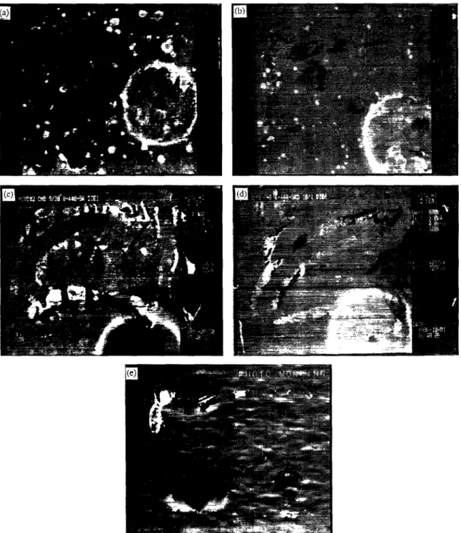
In order to optimize endpoint detection for tungsten plug pattern wafer polishing, a Hitachi in-line SEM system was used for the wafer surface examination. The temperature pro- file of W-CMP with QCTTIOI 1 slurry was used for this examination. Five patterned wafers with the same film stack
and structure were polished. The polishing times to stopproc- ess were set as 89, 92, 94, 96, and 106 s and then followed the cleaning process. The SEM images of the above five process time results are shown in Fig. 6(a)-(e) . In Fig. 6(d) , it is shown that 4 s over-polishing (96 s polishing time, the time to temperature peak was 92 s) after the pad temperature peak is necessary for the full removal of all metal film resi-
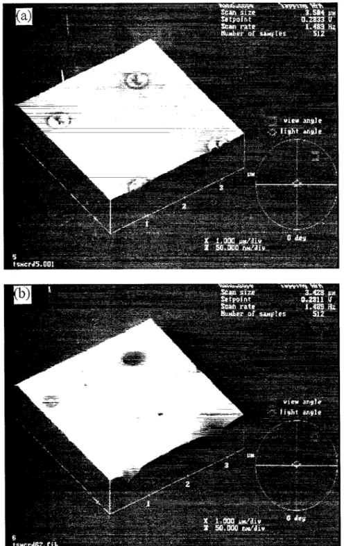
dues. However, the 13 s over-polishing results in a W-plug loss and recess, as shown in Fig. 6(e). The surface roughness after W-CMP was also measured by atomic force microscopy (AFM). Fig. 7(a) and (b) shows the AFM images of 1 and 14 s over-polishing after the pad temperature peak. It is shown that the surface of the 4 s over-polishing has smoother W-plug profile without oxide roughness and scratch ( see Fig. 7(a) ). The surface of the 14 s over-polishing shows W-plug loss, recess and oxide roughness as well as oxide scratch due to over-polishing. It is thought that the W-plug recess is
caused by the erosion of W slurry and the oxide roughness and scratch are caused by the Al,O, abrasive particles with the over-polishing time. Here. a conclusion can be made that over-polishing without a proper endpoint detection algorithm could cause W plug loss, oxide roughness and scratch. With the above study. the pad temperature trend offers a good way as an endpoint detection algorithm and results in a smooth W plug as well as no roughness and scratch on the oxide surface. The relation between the temperature profile and process parameter such as down force and platen speed was also
Y.-L. Wang rt al. /Muterids Cilemisty and Physics 52 (1998) 17-22
m-P=5 psi,V=50 cpm - - - P=8 pri.V=5, ‘pm
r--I
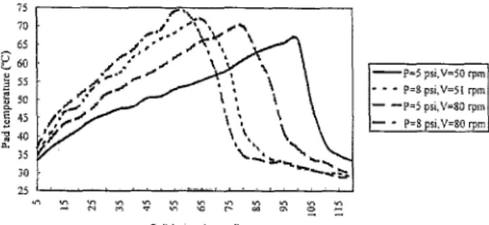
- -P-5 psi,V=SO ‘pm - - P-8 p.v=*o rpmFig. 8. The pad temperature protile during wafers polishing for different process parameters.
Table 4
The removal rate and non-uniformity for different down force and platen speed
Condition Removal rate (A mitt- ‘) Non-uniformity (S’c) p=5psi,r,=50rpm 3560 4.5 p=8psi,~=50rpm 5482 12.5 p=5psi,L,=80rpm 4502 16.7 p = 8 psi, ~3 = 80 rpm 6174 21.8
investigated. Fig. 8 shows the temperature profile of different down force (psi) and platen speed (rpm) using the QCTTlOl 1 slurry for polishing. Table 4 also shows the removal rate and non-uniformity by measuring the thickness of the blanket wafers which have the same polishing condi- tion as the patterned wafers.
In Table 4, the increase of down force or platen speed exhibit a higher polishing removal rate yet result in poor uniformity. In Fig. 8, it is also shown that higher down force or platen speed result in higher pad temperature profile and a shorter time to reach the peak, but the temperature drops slowly after the peak. It is believed that &he poor uniformity is responsible for this behaviour of temperature curve. Under the conditions of higher down force or platen speed, the polishing process directly after the peak of temperature curve exists some residue of metal film on the oxide surface because
of the non-uniformity. The effect of this non-uniformity needs further over-polishing time to remove the metal resi- due. Therefore, a steep temperature drop after the peak indi- cates a good polishing uniformity and a gradual slope indicates a poor polishing uniformity.
4. Conclusions
A new endpoint detection technique for the W-CMP proc- ess is presented. This novel method can be used to monitor the polishing history during the W-CMP process by meas- uring the pad temperature. From the temperature curve, the endpoint can be clearly detected and the process can be stopped at the oxide layer. Smooth W-plug without oxide roughness and scratch patterned wafer has been shown by SEM and AFM images with the use of this new endpoint detection system. Also, this method studied the effects of CMP process conditions such as down force, platen speed as well as polishing performance such as removal rate and uni- formity. This new method is simpler, less expensive and more successful than other endpoint detection techniques which exist in semiconductor industry today.
References I11 I21 [31 iJ1 151 [61 171 [81 [91
W.J. Patrick, W.L. Guthrie, C.L. Standley and P.M. Schiable, J. Elec- trocbem. Sot., 138 (6) ( 1991) 1778.
M.A. Fury, Solid State Technol., (1995) 47.
F.B. Kaufman, O.B. Thompson, R.E. Broadie, M.A. Jaso, W.L. Guth- rie, D.J. Pearson and M.B. Small. J. Electrochem. Sot., 138 ( 11) ( 1991) 3460.
C. Yu, S. Poon, Y. Limb, T. Yu and J. Klein, Proceedings of VLSI Multilevel Interconnect Conference (VMIC), 1994, p. 144. S. Roy, Advanced Merallization and Interconnect Systems for ULSI Applications, 1995, p. 733.
CC. Yu et al., U.S. Patent, No. 5240552. W.J. Cote et al., U.S. Patent, No. 5308438. D.A. Koos et al.. U.S. Patent, No. 5113941.
M. Rutten, P. Feeney, R. Cheek and W. Landers, Semiconductor Int., (1995) 122.