Effects of Nitrogen Plasma Treatment on Tantalum Diffusion
Barriers in Copper Metallization
Wen-Fa Wu,a,
*
,zKeng-Liang Ou,bChang-Pin Chou,band Chi-Chang Wua
a
National Nano Device Laboratories, Hsinchu 300, Taiwan
bInstitute and Department of Mechanical Engineering, National Chiao-Tung University, Hsinchu 300, Taiwan
In this study, the barrier properties of ultrathin Ta, TaN, and nitrogen plasma-treated Ta films were investigated by Cu/Ta共N兲/Si structure. The barrier properties were evaluated by sheet resistance, film stress, X-ray diffraction, transmission electron micros-copy, scanning electron microsmicros-copy, atomic force microsmicros-copy, and X-ray photoelectron spectroscopy. Nitrogen plasma-treated Ta films possess better barrier performance than sputtered Ta and TaN films. The sheet resistance of Cu/Ta/Si and Cu/TaN/Si increases, apparently, after annealing at 600 and 625°C, respectively. The Cu/30 min plasma-treated Ta/Si is fairly stable up to annealing at 700°C for 1 h. Diffusion resistance of the plasma-treated Ta barrier is more effective. It is believed that a new amorphous layer forms on the surface of Ta film after plasma treatment. The new amorphous layer possesses some nanocrystalline Ta2N phases with lattice constant 0.305 nm. It is believed that the amorphous layer containing some nanocrystals can alleviate Cu diffusion into the Si substrate and, hence, improve barrier performance.
© 2003 The Electrochemical Society. 关DOI: 10.1149/1.1531974兴 All rights reserved.
Manuscript submitted October 1, 2001; revised manuscript received May 28, 2002. Available electronically January 2, 2003.
Copper is an attractive material for interconnection due to its lower electrical resistivity and better electromigration resistance compared to Al-based alloys. Copper is better considered for appli-cation in integrated circuits. However, it is well known that copper diffuses quickly in Si substrates and SiO2films, which causes deg-radation of transistor reliability by forming particular impurity levels in the silicon.1Because of its ability to rapidly diffuse in silicon and degrade reliability, the development of effective diffusion barrier materials is the most important issue for the realization of Cu inter-connection in Si-based integrated circuits. Many materials are used as diffusion barriers in copper metallization system. Refractory met-als and their nitrides have been investigated for such applications. Among them, tantalum and tantalum nitride have received the most attention owing to their high thermal stability and resistance to form compounds with copper. Previous studies have shown that tantalum nitride is more desirable than tantalum in terms of barrier effective-ness. However, resistivity of tantalum nitride film is higher than that of tantalum film.2-4As the technology moves to 180 nm node and below, a thin barrier layer is necessary to lower the resistance of the total line interconnect and/or via. It becomes inappropriate to use a barrier layer thicker than 30 nm, and hence investigations of the thermal stability and barrier properties of ultrathin barrier layers in the Cu metallization system are important.
In this article, we studied the barrier properties and thermal sta-bility of ultrathin Ta-based barrier layers共10 nm兲 in the Cu metal-lization system. Furthermore, a new method to form nitrogen incor-porated Ta film with low resistivity and high thermal stability was proposed and investigated. Nitrogen plasma was used to post-treat the Ta diffusion barrier. Properties of barrier layers were evaluated by electrical measurements and material analyses.
Experimental
The substrates used in these experiments were p-type共100兲 ori-ented silicon wafers with resistivity of 5-10⍀ cm. The Si wafers were cleaned in a dilute HF solution (HF:H2O⫽ 1:20) for 2 min, and rinsed in deionized共DI兲 water prior to loading into the sputter-ing system. The 10 nm Ta films were deposited at a power of 500 W and a sputtering pressure of 6.4 mTorr after the base pressure was evacuated to below 5⫻ 10⫺7Torr. Some wafers further received ex situ nitrogen plasma treatments in a plasma enhanced chemical va-por deposition共PECVD兲 system after tantalum films were depos-ited. In addition, 10 nm tantalum nitride films were also deposited
by reactive sputtering for comparison. The tantalum nitride films were prepared using optimum conditions as in our previous investi-gations, and thus provided a more effective barrier against Cu diffusion.2For easy identification, the sputtered tantalum, tantalum nitride, and nitrogen plasma-treated tantalum films were denoted as Ta, TaN, and TaNx/Ta. Copper films, 300 nm thick, were deposited
on top of the barrier layers. Cu/Ta/Si, Cu/TaN/Si, and Cu/TaNx/Ta/Si were annealed in N2ambient from 500 to 800°C for 1 h to evaluate the thermal stability.
To realize the properties of Ta-based barrier layers, they were analyzed by atomic force microscopy共AFM兲, sheet resistance, and film stress. The film stress was obtained by measuring the changes in the radius of curvature of the substrate using laser scanning tech-nology. In addition, X-ray photoelectron spectroscopy共XPS兲 using monochromatized Mg K␣ radiation was performed to identify the chemical states of tantalum films with N2 plasma treatments. To realize the capability of barrier layer against copper diffusion, the microstructure was observed using transmission electron micros-copy 共TEM兲. Surface morphology of annealed Cu/barrier/Si was observed by scanning electron microscopy共SEM兲. Compositions of failure sites were analyzed by energy-dispersive spectrometry共EDS兲 after removing both copper and barrier layers with a wet chemical solution. Grazing incidence X-ray diffractometry共GIXRD兲 was
car-*Electrochemical Society Active Member.
zE-mail: [email protected]
Figure 1. XRD spectra of sputtered and nitrogen plasma-treated Ta共10 nm兲
films.
) unless CC License in place (see abstract). ecsdl.org/site/terms_use
address. Redistribution subject to ECS terms of use (see 140.113.38.11
ried out for phase identification. The incident angle of the X-ray was fixed at 3°. Cu/barrier/n⫹-p junction diodes with conventional local-ized oxidation of silicon 共LOCOS兲 isolation were fabricated for electrical analyses. Leakage currents of the diodes were measured by HP4145B semiconductor parameter analyzer at a reverse bias of ⫺5 V. After annealing at various temperatures for 1 h, the diode leakage current was measured.
Results and Discussion
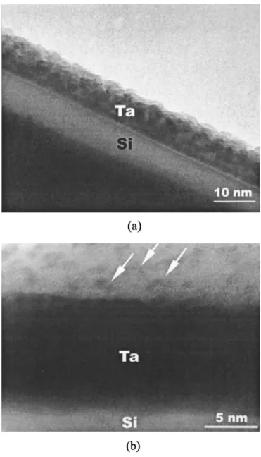
Properties of N2 plasma-treated Ta films.—Figure 1 shows the X-ray diffraction共XRD兲 spectra of 10 nm Ta films with and without plasma treatments. The time shown in the parenthesis is the period of the nitrogen plasma treatment. The intensity and shape of reflec-tion indicate changes in the phase of the Ta film. By XRD analyses, it is obvious that as plasma-treatment time increases, the peak shape of body-centered cubic 共bcc兲-Ta共N兲共110兲 phase becomes broad gradually. The phenomenon indicates lattice distortion and/or devel-opment of an amorphous Ta共N兲 thin film after plasma treatment. Figure 2 shows cross-sectional TEM micrographs of 30 min plasma-treated Ta/Si. The development of an amorphous TaNxlayer on the
film surface was observed after the plasma treatment. The thin
amor-phous layer possesses some nanocrystalline Ta2N phases 共denoted by arrows兲 with lattice constant 0.305 nm, as shown in Fig. 2b. Chemical bonding states of Ta films with N2plasma treatments were analyzed by XPS. Figure 3 shows the Ta 4f spectrum of the Ta film with the N2plasma treatment for 5 min. In compared with the Ta 4f peak of metal tantalum in the Handbook of X-Ray Photoelectron Spectroscopy,55 min plasma-treated Ta film关denoted as TaNx/Ta共5
min兲兴 indicates a chemical shift of 0.6 eV. It is attributed to the formation of Ta-N bond, which corresponds well to the value of the chemical shift reported as Ta2N in the article.6It reveals that the chemical state of Ta2N compound forms after the N2plasma treat-ment. Figure 4 shows the N 1s spectra of Ta films with various plasma-treatment time. It can give information concerning nitrida-tion effects. Significant changes in N 1s peak are observed for Ta films with various plasma-treatment time. With N2 plasma treat-ments, one peak at ⬃398 eV is found in the N 1s spectrum. It is attributed to N␦⫺, which is similar to the nitride ion.7,8The presence of the N 1s peak in Fig. 4 shows clearly that the surface is nitrided by nitrogen plasma. As the N2plasma treatment time increased to 30 min, another N 1s peak at⬃401 eV is found in the N 1s spectrum. The peak at⬃401 eV is ascribed to the nitrogen atoms or molecules Figure 2. 共a兲 Cross-sectional TEM micrograph of 30 min plasma-treated Ta
共10 nm兲/Si. 共b兲 Corresponding high resolution TEM micrograph.
Figure 3. Ta 4f XPS spectrum obtained from the Ta film with nitrogen
plasma treatment of 5 min.
Figure 4. N 1s XPS spectra obtained from the Ta films with nitrogen plasma
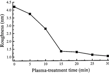
present in interstitial sites. This kind of nitrogen is also detected in tungsten films prepared by the reduction of WF6with N2in nitrogen gas.8These results indicate that some N atoms do not form strong covalent or ionic bonds with Ta atoms during the plasma nitridation of Ta film. Some of the introduced N atoms segregate at the inter-stitial sites and grain boundaries in the tantalum film as impurities. Similar results were reported for plasma nitridation of chemical va-por deposited共CVD兲 tungsten by Chang et al.7This result is con-sistent with high-resolution共HR兲 TEM observation. As the plasma-treatment time increases, the amorphous layer with Ta2N nanoparticles embedded inside was formed. Figure 5 shows root-mean-square 共rms兲 surface roughness as a function of plasma-treatment time. The surface roughness is measured by AFM. It can be seen that the longer the plasma-treatment time, the smoother the surface. The surface roughness of as-sputtered Ta and TaNx/Ta共30
min兲 films are 4.21 and 1.08 nm, respectively. It is believed that sputtering and/or stuffing effects would occur due to the reactions or bombardments of energetic radicals and ions during plasma treat-ment. They could sputter the films and make them smooth. Nitrida-tion effects also occur during nitrogen plasma treatment. Chemical compositions of plasma-treated tantalum films were analyzed by XPS. It is found that nitrogen content increases with increasing plasma-treatment time. Nitrogen content of the Ta film with 5 min plasma treatment is 5.64 atom %. With plasma treatment for 30 min, nitrogen content is 32.12 atom %. Figure 6 shows stress of TaNx/Ta
barrier as a function of plasma-treatment time. After N2 plasma
treatment for 5 min, a high compressive stress developed in the TaNx/Ta barrier. The stress transforms from compressive to tensile
for films with N2plasma treatments longer than 15 min. The com-pressive stress could result from the lattice distortion, produced by incorporation of nitrogen atoms of a size different from the Ta film, and reaction and stuffing at grain boundaries. Atomic peening effect would induce compressive stress in plasma process. However, with further increase in the period of the nitrogen plasma treatment, amorphous films were formed and the stress becomes tensile. Figure 7 shows normalized resistivity of Ta films before and after plasma treatments.
The normalized resistivity is designated as the ratio of R to Ro (R/Ro), where Roand R denote the resistivity of as-sputtered and plasma-treated Ta films, respectively. The resistivity of as-deposited Ta film is 197⍀ cm. As plasma-treatment time increased from 5 to 15 min, the resistivity decreased initially and then increased. How-ever, resistivity of 30 min plasma-treated Ta film does not increase further. In our previous study, it is found that resistivity of the reac-tively sputtered TaN film would initially decrease to 159⍀ cm and then increase to higher than 3500 ⍀ cm as nitrogen flow ratio increases during reactive sputtering.2Min et al. reported similar re-sults. It is found that small nitrogen incorporation could result in the decrease of the resistivity of reactively sputtered Ta共N兲 film.9The formation of the amorphous layer would increase the resistivity due to increasing scattering effects. The variation in resistivity is due to the combined effects as mentioned above. The nitrogen incorpora-Figure 5. RMS surface roughness of Ta thin film as a function of
plasma-treatment time.
Figure 6. Stress of plasma-treated Ta/Si as a function of plasma-treatment
time.
Figure 7. Normalized resistivity of TaNx/Ta as a function of
plasma-treatment time.
Figure 8. Variation in sheet resistance of Cu/Ta共N兲/Si as a function of
an-nealing temperature.
) unless CC License in place (see abstract). ecsdl.org/site/terms_use
address. Redistribution subject to ECS terms of use (see 140.113.38.11
tion is the dominant factor in the early plasma treatment. Resistivity would increase due to the development of the amorphous layer after increasing plasma treatment.
Thermal stability of Cu/Ta(N)/Si.—Figure 8 shows the variation in sheet resistance of Cu/Ta共N兲/Si as a function of annealing tem-perature. The data mainly indicates changes in the thickness or re-sistivity of the unreacted copper layer, since the resistance of the barrier layer and reaction products are expected to be much larger than that of Cu. It is found that sheet resistance of annealed Cu/ barrier/Si is slightly lower than that of as-deposited after low tem-perature annealing. It is acribed to a decrease in defect density and grain growth of Cu film.1Low sheet resistance is obtained for all samples before they are annealed at the failure temperature. In the study, the failure temperature is defined as the temperature that the great increase of sheet resistance is found after annealing. As shown in Fig. 8, the sheet resistance of Cu/Ta/Si increases greatly after annealing at 600°C. Moreover, a change in color of copper surface and production of precipitate are found. It reveals that significant reactions have occurred between the layers. The increase of sheet resistance may also result from agglomeration of copper film after annealing. No obvious change in sheet resistance was observed for Cu/TaN/Si at the annealing temperature of 600°C. However, great increase is also found after annealing at 625°C. Cu/TaNx/Ta/Si
re-mains low sheet resistance even after annealing at 700°C for 1 h. It is obvious that an N2 plasma-treated Ta (TaNx/Ta) barrier layer
possesses higher thermal stability than Ta and TaN barrier layers. XRD analyses are performed to identify the phase formation of the Cu/Ta共N兲/Si samples after high temperature annealing. Figure 9 il-lustrates the XRD spectra for Cu/Ta/Si, Cu/TaN/Si, and Cu/TaNx/Ta/Si samples subjected to anneal at various temperatures.
Strong Cu共111兲, and weak Cu共200兲 peaks are observed in as-deposited and annealed samples, indicating that the Cu films have preferred具111典crystal orientation. It has been reported that Cu with high具111典texture provides higher electromigration resistance.10For the Cu/Ta/Si sample annealed at 550°C, signals of TaSi2and Cu3Si phases are detected. After annealing at 600°C, the signal of Cu dis-appeared while peaks of Cu3Si increase obviously, indicating the failure of the Ta barrier layer. The high resistivity Cu3Si formation and related Cu decrease resulted in the great increase of sheet resis-tance as shown in Fig. 8. For the sample with the TaN barrier layer, a Cu3Si phase was detected after annealing at 625°C. In contrast to Cu/Ta/Si, peaks of Cu were still observed after annealing at 625°C for 1 h. Clearly, thermal stability of the Cu/TaN/Si is superior to that of the Cu/Ta/Si contact system. XRD results of Cu/TaNx/Ta/Si
samples show that the crystallization of the amorphous-like TaNx
layer occurs after annealing at 600°C. As shown in Fig. 9c, Ta2N and TaSi2phases were detected after annealing at 600 and 700°C, respectively. After annealing at 750°C for 1 h, peaks of Cu3Si are detected. In respect of the phase formation of tantalum silicide, the formation temperature of the sample with TaNx/Ta barrier was
Figure 9. XRD spectra for 共a兲 Cu/Ta/Si, 共b兲 Cu/TaN/Si, and 共c兲
Figure 10. 共a兲 SEM micrograph of Cu/Ta共N兲/Si sample annealed at failure
temperature.共b兲 Enlarged image of the precipitate. 共c兲 EDS spectrum ob-tained from the precipitate.
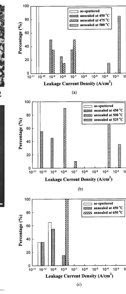
Figure 11. Distributions of leakage current density of the共a兲 Cu/Ta/Si, 共b兲
Cu/TaN/Si, and共c兲 Cu/TaNx/Ta/Si n⫹-p junction diodes after annealing at
various temperatures for 1 h.
) unless CC License in place (see abstract). ecsdl.org/site/terms_use
address. Redistribution subject to ECS terms of use (see 140.113.38.11
higher than that of the sample with Ta or TaN barrier. That is, nitro-gen plasma treatment will restrain formation of tantalum silicide, attributed to formation of a nanostructured amorphous barrier layer to alleviate Cu diffusion. It was reported that Cu penetration would promote Ta silicide formation.11Table I summarizes XRD results of Cu/Ta/Si, Cu/TaN/Si, and Cu/TaNx/Ta/Si after annealing at various
temperatures for 1 h. The failure temperatures of Ta, TaN, and TaNx/Ta barrier layers are 600, 625, and 750°C, respectively. It is
found that phases of copper silicide and tantalum silicide were de-tected after annealing at the failure temperature. For further analysis of the thermal stability, SEM was used to examine the surface mor-phologies of Cu films after thermal annealing. After annealing at the temperature higher than the failure temperature, protrusions or pre-cipitates were observed on the surface. Figure 10 shows the typical SEM micrographs of Cu/barrier/Si after annealing at the temperature higher than the failure temperature. As shown in Fig. 10a, protru-sions are observed on the surface, indicating a severe reaction of Cu/barrier/Si. Figures 10b and c show enlarged image of the protru-sion and corresponding EDS spectrum. It reveals that the protruprotru-sion consisted of elemental Cu and Si, and was a copper-rich region.
These protrusions are presumably caused by Cu diffusion through the localized weak point in the barrier and reacting with underlying Si to form Cu3Si. Similar phenomena were reported for Ta diffusion barriers by Hollway et al.11Barrier capabilities of ultrathin Ta, TaN, and TaNx/Ta films are further investigated by evaluating the thermal
stability of Cu/barrier/n⫹-p junction diodes using electrical mea-surements. Figure 11 illustrates the statistical distributions of reverse biased leakage current densities for Cu/barrier共10 nm兲/n⫹-p junc-tion diodes annealed at various temperatures. If we define a failure criterion with 10⫺6 A/cm2, the Cu/Ta/n⫹-p diodes remain stable after annealing at temperatures up to 475°C but suffered degradation at 500°C 共Fig. 11a兲. It is reported that the barrier properties of Ta can be improved by adding impurities, such as N and O.2,4,12Figure 11b shows the statistical distributions of reverse biased leakage cur-rent densities for the Cu/TaN/n⫹-p junction diodes annealed at vari-ous temperatures. For the diodes with 10 nm TaN barriers, the di-odes remained stable after annealing at temperatures up to 500°C. After annealing at 525°C, failure of the diodes was observed. Tsai et al. reported similar results. It was found that the diodes with 60 nm CVD and physical vapor deposited TaN barriers would begin to deteriorate at 500 and 550°C, respectively.12It is shown that barrier capability of TaN film is better than that of Ta film. However, the improvement is limited. Furthermore, the resistivity of reactively sputtered TaN will increase significantly with increasing nitrogen concentration. The resistivity of the TaN film sputtered at 35% ni-trogen flow ratio would increase to⬃3500 ⍀ cm, from ⬃190 ⍀ cm for the Ta film.2As mentioned previously, nitrogen incorporated Figure 12. Cross-sectional TEM micrographs of共a兲 550°C-annealed Cu/Ta/
Si,共b兲 Cu3Si precipitates, 共c兲 625°C-annealed Cu/TaN/Si, and 共d兲 600°C-annealed Cu/TaNx/Ta/Si.
Figure 13. HRTEM micrograph of Cu/TaNx/Ta interface in Cu/TaNx/Ta/Si sample after annealing at 600°C for 1 h.
Figure 14. Schematic illustrations of
the microstructures of共a兲 Cu/Ta/Si 共b兲 Cu/TaN/Si, and 共c兲 Cu/TaNx/Ta/Si samples before and after annealing.
Ta films (TaNx/Ta) were also prepared by nitrogen plasma
treat-ment in the study. The resistivity of TaNx/Ta was as low as that of
as-sputtered Ta, as shown in Fig. 7. The Cu/TaNx/Ta/n⫹-p diodes
retained electrical integrity even after annealing at 650°C, as shown in Fig. 11c. The TaNx/Ta films possess much better barrier
perfor-mance than Ta and TaN films. The improved barrier perforperfor-mance is attributed to nanocrystallization and stuffing effects due to the reac-tions or bombardments of energetic radicals and ions during plasma treatment. It is reported that the microstructure within the barrier layer strongly affects the barrier performance because Cu diffuses through fast diffusion paths such as grain boundaries within the barrier layer.2,9,13The thin nanocrystalline TaNx layer was formed
on the surface of the Ta film after nitrogen plasma treatment, as shown in Fig. 2. A Nanostructured diffusion barrier is more effective for preventing Cu diffusion than a polycrystalline barrier because the nanostructured film does not have large-angle grain boundaries where most of the atomic diffusion typically occurs.14
Failure mechanism of Cu/Ta(N)/Si.—It is obvious that there ex-ists the difference of failure mechanism among Ta, TaN, and TaNx/Ta barriers as shown in the results of sheet resistance
mea-surements and XRD analyses. Figure 12 shows cross-sectional TEM micrographs of annealed Cu/Ta/Si, Cu/TaN/Si, and Cu/TaNx/Ta/Si.
As shown in Fig. 12a, it is obvious that Ta silicide and Cu silicide were observed after annealing, and the interface of the sample is not clear. It indicates the degradation of the Ta barrier after annealing at 550°C for 1 h. The as-deposited Ta film consists of fine (⬃20 nm兲 columnar grains. The degradation of the Ta barrier is attributed to the diffusion of Cu into the Si substrate through the columnar Ta barrier. Figure 12b illustrates the corresponding image of the Cu3Si precipitate in the Si substrate. Trapezoidal-shaped copper silicide spikes bounded by Si兵111其 and Si兵001其 planes are observed.11Figure 12c shows the TEM image of the Cu/TaN/Si sample after annealing at 625°C for 1 h. The multilayered structure is destroyed and trian-gular and trapezoidal Cu3Si precipitates form with the disappearance of Cu overlay. It indicates degradation of the TaN barrier at 625°C. Figure 12d shows the TEM image of Cu/TaNx/Ta/Si sample after
annealing at 600°C for 1 h. There exists an amorphous layer be-tween the Cu and Ta-based barrier layers. Neither Cu silicide nor Ta silicide were observed at the interface, which shows the excellent barrier properties. The corresponding high resolution TEM image of annealed Cu/TaNx/Ta/Si sample, is shown in Fig. 13. It indicated
that the nanocrystalline Ta2N phase appears within the amorphous layer. Furthermore, microtwins共denoted as narrows兲 are found at Ta and Ta2N interface.
Cross sections of the interfacial structures before and after an-nealing are shown schematically in Fig. 14a, b, and c for the Cu/Ta/ Si, Cu/TaN/Si, and Cu/TaNx/Ta/Si samples, respectively. Cu films
on Ta, TaN, and TaNx/Ta barriers have preferred兵111其 orientation.
The as-deposited Ta barrier has a Ta bcc structure with fine (⬃20 nm兲 columnar grains as shown in Fig. 14a. Formation of TaSi2 and copper silicide were observed after annealing at 550°C for 1 h, indicating the barrier degradation. The mechanism by which the barrier fails is the motion of Cu through the columnar Ta to form Cu3Si. The barrier capability of the Ta film against Cu diffusion can be improved by incorporating nitrogen in the Ta film using reactive sputtering. The structure of the reactively sputtered TaN films will change from voided columnar to fibrous and featureless with in-creasing nitrogen flow ratio, and the TaN film with amorphous-like structure functions as a more effective barrier against Cu diffusion.2,15The as-deposited TaN barrier has a Ta共N兲 bcc structure,
as shown in Fig. 14b. No Cu silicide is observed for Cu/TaN/Si sample after annealing at 600°C for 1 h, indicating better barrier property than that of Ta. However, the barrier capability of the Ta film is improved moderately by incorporating nitrogen with reactive sputtering. Similar trapezoidal or triangular Cu3Si precipitates formed with the disappearance of Cu overlay after annealing at 625°C for 1 h, as shown in Fig. 14b. The formation of a thin amor-phous TaNx layer on the surface of Ta film is observed after the
nitrogen plasma treatment. The TaNx/Ta barrier prevented the Cu/Si
reaction as shown in Fig. 14c. There exists an amorphous layer between the Cu and barrier layers after annealing at 600°C for 1 h. The barrier retains its integrity and no Cu silicide or Ta silicides were observed. Nanocrystallization and stuffing effects of plasma treatments would alleviate the Cu diffusion and hence enhance bar-rier stability. High thermal stability of Cu/TaNx/Ta/Si is obtained.
Conclusion
Nitrogen incorporated Ta films (TaNx/Ta) were prepared by
ni-trogen plasma treatment. The resistivity of TaNx/Ta was as low as
that of as-sputtered Ta film. Barrier properties of TaNx/Ta are better
than those of sputtered Ta and TaN. As plasma-treatment time in-creases, the surface roughness decreases obviously. Nanocrystalliza-tion and stuffing effects as well as nitridaNanocrystalliza-tion were observed. With the reactions and bombardments of nitrogen ions and radicals, a new amorphous layer induces on the surface of the Ta barrier. The barrier stability of the Ta films enhanced apparently after nitrogen plasma treatment. The Cu/TaNx/Ta共10 nm兲/Si remained stable after
anneal-ing at 700°C for 1 h. The failure temperature of TaNx/Ta barrier is
at least 150°C higher than that of the Ta barrier. Nanocrystallization and stuffing effects of plasma treatments are believed to impede Cu diffusion into the Si substrate and, hence, improve the barrier performance.
Acknowledgments
The authors would like to thank the National Science Council of Republic of China for financially supporting this research under contract no. NSC 90-2215-E-317-005 and NSC 91-2722-2317-200. National Nano Devices Laboratories assisted in meeting the publication costs of this article.
References
1. Y. J. Lee, B. S. Suh, M. S. Kwon, and C. O. Park, J. Appl. Phys., 85, 1927共1999兲. 2. W. L. Yang, W. F. Wu, D. G. Lin, C. C. Wu, and K. L. Ou, Solid-State Electron., 45,
149共2001兲.
3. M. T. Wang, Y. C. Lin, and M. C. Chen, J. Electrochem. Soc., 145, 2538共1998兲. 4. X. Sun, E. Kolawa, J. S. Chen, J. S. Reid, and M. A. Nicolet, Thin Solid Films, 236,
347共1993兲.
5. J. F. Moulder, W. F. Stickle, P. E. Sobol, and K. D. Bomben, Handbook of X-Ray
Photoelectron Spectroscopy, p. 170, Physical Electronics, Inc., Eden Prairie, MN
共1995兲.
6. O. Ibidumni, R. L. MaSaitis, R. L. Opila, A. J. Davenport, H. S. Isaacs, and J. A. Taylor, Surf. Interface Anal., 20, 559共1993兲.
7. K. M. Chang, T. H. Yeh, I. C. Deng, and C. W. Shih, J. Appl. Phys., 82, 1469 共1997兲.
8. T. Nakajima, K. Watanable, and N. Watanabe, J. Electrochem. Soc., 134, 3175 共1987兲.
9. K. H. Min, K. C. Chun, and K. B. Kim, J. Vac. Sci. Technol. B, 14, 3263共1996兲. 10. Y. L. Chin, B. S. Chiou, and W. F. Wu, Jpn. J. Appl. Phys., Part 1, 39, 6708共2000兲. 11. K. Holloway, P. M. Fryer, C. Cabral, Jr., J. M. E. Harper, P. J. Bailey, and K. H.
Kelleher, J. Appl. Phys., 71, 5433共1992兲.
12. M. H. Tsai, S. C. Sun, C. E. Tsai, S. H. Chuang, and H. T. Chiu, J. Appl. Phys., 79, 6932共1996兲.
13. G. S. Chen and S. T. Chen, J. Appl. Phys., 87, 8473共2000兲. 14. D. J. Kim, Y. T. Kim, and J. W. Park, J. Appl. Phys., 82, 4847共1997兲. 15. G. S. Chen, P. Y. Lee, and S. T. Chen, Thin Solid Films, 353, 264共1999兲.
) unless CC License in place (see abstract). ecsdl.org/site/terms_use
address. Redistribution subject to ECS terms of use (see 140.113.38.11