Magneto-optical response of layers of semiconductor quantum dots and nanorings
O. VoskoboynikovDepartment of Electronic Engineering and Institute of Electronics, National Chiao Tung University, 1001 Ta Hsueh Road, Hsinchu 300, Taiwan
C. M. J. Wijers
Faculty of Applied Science, University of Twente, P.O. Box 217, 7500 AE Enschede, The Netherlands
J. L. Liu
Department of Applied Mathematics, National Chiao Tung University, 1001 Ta Hsueh Road, Hsinchu 300, Taiwan
C. P. Lee
Department of Electronic Engineering and Institute of Electronics, National Chiao Tung University, 1001 Ta Hsueh Road, Hsinchu 300, Taiwan
共Received 17 February 2005; published 30 June 2005兲
In this paper a comparative theoretical study was made of the magneto-optical response of square lattices of nanoobjects共dots and rings兲. Expressions for both the polarizability of the individual objects as their mutual electromagnetic interactions共for a lattice in vacuum兲 was derived. The quantum-mechanical part of the deri-vation is based upon the commonly used envelope function approximation. The description is suited to inves-tigate the optical response of these layers in a narrow region near the interband transitions onset, particularly when the contribution of individual level pairs can be separately observed. A remarkable distinction between clearly quantum-mechanical and classical electromagnetic behavior was found in the shape and volume de-pendence of the polarizability of the dots and rings. This optical response of a single plane of quantum dots and nanorings was explored as a function of frequency, magnetic field, and angle of incidence. Although the reflectance of these layer systems is not very strong, the ellipsometric angles are large. For these isolated dot-ring systems they are of the order of magnitude of degrees. For the ring systems a full oscillation of the optical Bohm-Ahronov effect could be isolated. Layers of dots do not display any remarkable magnetic field dependence. Both type of systems, dots and rings, exhibit an outspoken angular-dependent dichroism of quantum-mechanical origin.
DOI: 10.1103/PhysRevB.71.245332 PACS number共s兲: 73.21.⫺b, 75.20.Ck, 75.75.⫹a
I. INTRODUCTION
It has been known for a long time that microstructured materials can manipulate electromagnetic radiation. Most of the research in that field focuses at present on photonic crys-tals, a concept introduced a long time ago.1 It is known al-ready that microstructured materials can act as photonic crys-tals. Recent advances in lithography, colloidal chemistry, and epitaxial growth have made it possible to manufacture artifi-cial meta-materials from semiconductor nano-objects. Fur-ther application of these materials in technology demands the extension of the usable frequency range. These demands will push research efforts in this field to the limit. Scale reduction is the classical answer to meet these increased frequency demands and that holds particularly for the new nanostruc-tured metamaterials. When these metamaterials can be made to manipulate electromagnetic fields in the optical range, this will be particularly beneficial for potential applications and devices, as well as for new basic science. The short list of possible implementations being at close range, consists of realization of optical quantum computing, metamaterials with negative refractive index2,3in the optical region, artifi-cial magnetism in basically nonmagnetic materials4and fur-ther.
Semiconductor quantum dots and nanorings are nanosized objects resembling artificial atoms.5,6 From these nanoob-jects, the nanorings are the newest and they are topologically different from quantum dots since their geometry is nonsim-ply connected. This different and unique topology gives them unusual magnetic and magnetooptical properties.6 The key characteristic of this topology, the center hole, enables trap-ping of magnetic flux quanta. This property of the nanorings leads to quantum oscillating behavior of the magnetic re-sponse of the nanoring for varying magnetic field B, the Aharonov-Bohm共AB兲 effect.7For a simultaneously applied optical beam this gives rise to the optical AB effects,8,9 which can occur only in nanorings. Modification of material properties by means of a magnetic field is an inherent aspect of AB effects, including optical. This option is a prerequisite to make artificial materials, not resembling anything in na-ture, such as negative refractive index metamaterials.2
Up to now, most of the investigations done in the field of magneto-optical effects in nanorings has been about far-infrared 共FIR兲 spectroscopy or magnetophotoluminescence 共MP兲.4,10–13In these methods an additional stimulus has been used, apart from the electromagnetic beam, to determine the response of the rings. These stimuli can be the creation of an extrinsic carrier population 共FIR兲 or an electromagnetic beam of higher frequency共MP兲. In this sense those methods 1098-0121/2005/71共24兲/245332共12兲/$23.00 245332-1 ©2005 The American Physical Society
use preexcitation. The data obtained by these methods are very important, but actually only return averaged single na-noring information. For a quantitative characterization of the optical properties of nanoring-based metamaterials a highly developed optical spectroscopy, such as ellipsometry, and an advanced theoretical description are indispensable. Proper understanding and modeling of the collective electromag-netic response of nanoring layers requires a correct approach, taking into account their composite and discrete character.14,16 In addition, comparison of the collective magneto-optical response of metamaterials made from semi-conductor quantum dots and nanorings can provide impor-tant information about the basic physical distinctions be-tween these two types of systems.
II. THEORY
In this paper the collective electromagnetic properties of layers of semiconductor quantum dots and nanorings in the optical range will be studied theoretically. It will be shown that the optical AB effect inherent to the ring structures can enrich the optical properties of nanostructured metamaterials. To reach this goal the theory of optical effects will be devel-oped beyond the single共averaged兲 quantum dot and nanoring picture. It will turn out that, as a result, the magnitude of these effects is clearly within the range of a modern ellipso-metric setup.
A. Polarizability: Quantum mechanics
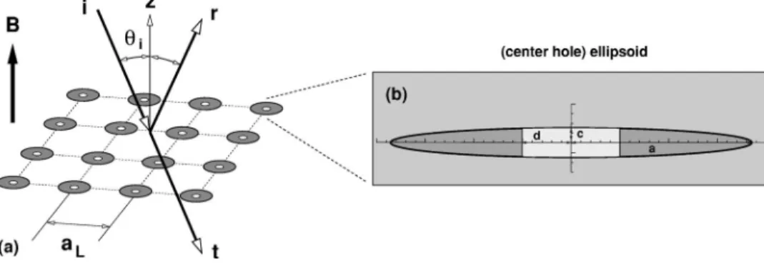
The systems to be investigated here are two dimensional square lattices of InAs/ GaAs quantum dots and nanorings, with lattice parameter aLas shown in Fig. 1. The basic ele-ments of those lattices are dots and “eye” shaped rings as obtained in recent experiments17,18 共Fig. 2兲. For their static electromagnetic response properties these elements will be modeled by means of ellipsoids共for the dots兲 or center hole ellipsoids共for the rings兲. This comparative study will use the same outer diameter and aspect ratio for the ellipsoid mod-eling of both bodies.
Quantum dots and rings are generally classified as artifi-cial atoms. Therefore their optical response should also be described in an atomiclike fashion, e.g., by means of polar-izabilities. For atoms such description has been developed originally by Kramers and Heisenberg19 and a multitude of derivations and modifications exist of this classical model. Optics in combination with quantum dot and ring structures
relies either upon expressions for optical absorption20 or for oscillator strengths,21,22 being the squared modulus of the optical transition matrix element.9 It is not straightforward, however, to transfer the Kramers-Heisenberg expressions to the case of a quantum ring or dot, described by means of envelope functions. To cope with the additional pitfalls we have 共re兲derived the Kramers-Heisenberg equations for this particular case.23The present commonly used description is only qualitative and the vector character of the electromag-netic response is not well described. Therefore we start this paper with a rehearsal of the main findings in Ref. 23.
To an arbitrary volume element V, containing material nanoobjects共dots/rings兲, an external electric field EX共r,t兲 of frequencyis applied. Electromagnetism requires this elec-tric field to be real valued and it has to be described by
EX共r,t兲 = EX共r兲cost = 1 2关e
it
+ e−it兴EX共r兲
and it has been shown in Ref. 23 that for such field the corresponding dipole strength d induced in the volume V, can be described by
具d典V共t兲 = Re关␣JG共兲EX共r兲e−it兴,
where␣Gis the total monochromatic polarizability. The ex-plicit expression for this monochromatic polarizability␣Gis given by23
FIG. 1. Schematic diagram of magneto-optical phenomena in a layer of nanorings. aLlattice
con-stant square lattice. Modeling of dots/rings by means of ellipsoids and center hole ellipsoids. a, c long and short axis, d radius cylin-drical center hole. i, r, t incoming, reflected, and transmitted beam, respectively.iangle of incidence.
FIG. 2. Typical shape of nanoring and quantum dot structures. 共a兲 Schematic InAs/GaAs “eye” shaped nanoring 关after TEM pic-ture共Ref. 17兲兴. 共b兲 Schematic InAs/GaAs “eye” shaped quantum dot关after TEM picture 共Ref. 18兲兴.
␣ JG共兲 = e2 ប
兺
lk 具k兩r兩l典V具l兩r兩k典V T flk共兲, flk共兲 =冉
2lk 冊
冋
关lk 2 −2−␥lk 2共兲兴 + i␥ lk共兲关lk 2 +2+␥lk 2共兲兴 关lk2 −2−␥lk2共兲兴2+ 4lk2␥lk2共兲册
, 共1兲where e is the electronic charge and具k兩r兩l典 is the transition matrix element. For each pair of levels l, k we have a tran-sition frequency lk and corresponding damping ␥lk.23 We have used explicitly that the expression for␥共兲 has to be even in. For its specific shape as a function ofhas been chosen: ␥lk共兲 =␥lk
冉
2lk 22 lk 4 +4冊
.This expression for␥lk共兲 is just modeling, done such that it is not much different from the traditional-independent␥in the region of resonance, where⬇lk, and resolves the sin-gularity problems in the near static regime, where ⬇0. Since it is in general not possible to obtain␥ in a theoreti-cally hard way, a simple algebraic format has been chosen to model it. Equation 共1兲 can be considered to be the “Swiss army knife” of discrete optics. In a twofold sense it is going to be used in this paper. First we will use it to derive an expression for the polarizability of a nanoring in the eneve-lope function approximation. Next we will use it to describe the bulk response of the same semiconductor material, the nanoobject is made from. Such relation is necessary to get an independent value for the matrix element controlling the na-noobject polarizability.
We will need for the two different systems, bulk and dot and ring, the following description for the quasiparticle states:
⌿TB共r兲 = eik·r共r兲, bulk,
⌿env共r兲 = F共r兲共r兲, nanoobject, 共2兲 where the bulk tight binding function共r兲 uses the conven-tional unit cell to define the periodic part of the Bloch states. For InAs the conventional cell consists of four elementary unit cells, each containing one In and one As atom. This cell is cubic and its size is given by the lattice constant ac. The bulk wave function has to be normalized over the volume of the conventional unit cell VB= ac
3, and the envelope function over the volume V. This ends up in the conditions
冕
VBdr兩共r兲兩2= 1,
冕
Vdr兩F共r兲兩2兩共r兲兩2= 1. 共3兲 We will need them for any quantitative determination of op-tical properties.
The first task is to determine the polarizability of a quan-tum dot or nanoring of volume V in the envelope function approximation. In this approximation the wave functions ⌿uk共r兲 of the nanoobject have to be written as
⌿uk共r兲 = Fuk共r兲u共r兲,
where Fuk共r兲 is the kth envelope function of the nanoobject belonging to the uthBloch state
u共r兲 of InAs 共or any other III-V compound from which the object is made兲. For u the value c will be used to describe the conduction and h to describe the valence band states, as before. The envelope function F共r兲 is dimensionless. In what follows the envelope function matrix element具Fuk兩Ful典V, will be defined as
具Fuk兩Ful典V= 1 VB
冕
V dr Fuk *共r兲F ul共r兲 =␦kl.The equality follows from combination of both equations in Eq.共3兲. Now the general expression for the polarizability of an arbitrary volume element 共1兲 needs to be applied to a nanoobject in the envelope function approximation and we need an expression for the optical matrix element具hk兩r兩cl典V. The Bloch states for the electron and hole states will be different and orthogonal. Then we have
具hk兩r兩cl典V=
兺
i NC Fhk*共ri兲Fcl共ri兲冋
ri冕
Vi dr⬘
h*共r⬘
兲c共r⬘
兲 +冕
Vi dr⬘
h *共r⬘
兲r⬘
c共r⬘
兲册
=具Fhk兩Fcl典Vrch, rch=冕
VB dr⬘
h *共r⬘
兲r⬘
c共r⬘
兲 = 具c兩r兩h典VB, 共4兲 where has been assumed that the entire nanoobject could be split into NC copies Vi of the conventional unit cell. Inside these cells Vi the envelope function is supposed to be con-stant. Using the expression for the matrix element共4兲 we can write the polarizability共1兲 as␣ JG= e2 បhk,cl
兺
兩具Fhk兩Fcl典V兩2关rch*rch T兴f hk,cl共兲.Since the optical matrix elements具c兩r兩h典VBdepend only upon the Bloch statesu, they do not depend on the indices k, l of the envelope states determined by the geometry of the na-noobjects. Hence,
␣ JG= e2 ប
兺
h,c rch*rchT兺
k,l 兩具Fhk兩Fcl典V兩2fhk,cl共兲. 共5兲 To each bulk stateubelong NCenvelope states. In the cal-culations to be done further in this paper only a very small number of these envelope states共typically six, three for the heavy hole and three for the electron states兲 being energeti-cally closest to the energy gap, will be used. This implies that the summation over c involves only the electronic spin ms. Such procedure is a good approximation for the imaginary part of the polarizability for energies near the band gap. For energies below this gap the polarizability is predominantly real and involves a summation over the tails of all pairs of states. The result of this summation, however, is almost con-stant as a function of frequency and can therefore be replaced by a constant value␣GS. In this approximation we obtain␣JG共兲 =␣JGS+ e2 បh,m
兺
s rch*rchT兺
k,l 3 兩具Fhk兩Fcl典V兩2fhk,cl共兲. 共6兲 The summation over bulk states is over the indices h, ms. For the nanosized objects investigated here, only transitions from heavy hole to electronic Bloch states will be taken into ac-count. The reason is that the dot-ring geometry causes the heavy and light hole states to be energetically different, even in the absence of a magnetic field B.The polarizability expression共6兲 embodies an intriguing hybrid of classical and quantum-mechanical thinking. The key ingredients of Eq.共6兲 are the static term ␣GS and any dynamic single pair contribution in the summation over kl. The␣GSdominates the repsonse for frequenciesbeing far below the energy gap EGand is explicitly shape and volume dependent. For any pair kl being at resonance共ប⬇Ekl兲 the polarizability is dominated by this single pair when the na-noobject and damping ␥kl are small enough 共the basic as-sumption of this paper兲. Then the polarizability depends only weakly, if at all, on shape and volume共there is a volume and shape effect through the energies Elk, but that effect has no influence on the strength of the polarizability as such兲. Any shape and volume dependence is only in the matrix element 具Fhk兩Fcl典V and that is in general not much different from 1. This shape and volume insensitivity of the strength of the polarizability under well observable resonance conditions is
a fully quantum-mechanical effect and finds its mirror in similar behavior known from conductance quantization24. The apparent and remarkable contrast in behavior of the two major components of the polarizability can be exploited to compare directly in one and the same system classical con-tinuous and quantized electromagnetic response.
To determine theoretically the required polarizabilities, asks for calculation of the electron and hole energies and wave functions, adjacent to the energy gap共the edge of op-tical absorption兲, for our nanoobjects in the presence of a magnetic field B 共see Fig. 3兲. It was found recently that experimentally relevant simulations of the behavior of the basic elements can only be obtained with three-dimensional models using the experimentally determined shape, strain and composition of the semiconductor nanoobjects.9,11,4 In the calculation used here, we assume that the electronic structure of these nanoobjects is governed by the hard-wall confinement potential due to the discontinuity in effective mass parameters over the edges of these objects themselves. This model is commonly used to calculate electron energy states in quantum heterostructures25 and allows us to solve the 3D Schrö dinger equation with a minor number of addi-tional approximations. This is particularly useful in this study where we concentrate on the collective optical proper-ties of systems of dots and rings.
Prior to writing the detailed description of the energetic structure of dots and rings we introduce the additional geo-metric index i:
i =共i兲,共e兲 共7兲
and where index u will be as defined before. If index i has value共i兲 it refers to the inner region of the dots and rings and with value 共e兲 to the surrounding embedding matrix. The effective envelope function Hamiltonian is given in the form
Hˆ = pc 1 2mu共E,r兲 pc+ Vi共r兲 +B gu共E,r兲 2 B, pc= − iបr+ eA共r兲, 共8兲 where pcstands for the electronic canonical momentum op-erator,ⵜr is the spatial gradient, and A共r兲 is the vector po-tential 共B= ⫻A兲. For electrons mc共E,r兲 and gc共E,r兲 are FIG. 3. Transition energy as a function of magnetic field B =共0,0,B兲 for k=l=0,−1,−2 optical transitions 共k→l兲 .
the energy- and position-dependent effective mass and Landé factor, respectively, 1 mc共E,r兲 =2P 2 3ប2
冉
2 E + Eg共r兲 − Vc共r兲 + 1 E + Eg共r兲 − Vc共r兲 + ⌬共r兲冊
, and gc共E,r兲 = 2冉
1 − m0 mc共E,r兲冋
⌬共r兲 3关E + Eg共r兲 − Vc共r兲兴 + 2⌬共r兲册
冊
,where Vc共r兲 is the confinement potential, Eg共r兲 and ⌬共r兲 stand for position-dependent energy band gap and spin-orbit splitting in the valence band, P is the momentum matrix element 共Kane parameter兲, and is the vector of the Pauli matrices. The free electron mass is m0. For the heavy holes mHH共E,r兲 and gHH共E,r兲 are assumed to be not energy depen-dent. The hard-wall confinement potential Vu is given for both electrons and holes by
Vu i共r兲 = 0, Vu e共r兲 = V u e . 共9兲
We consider cylindrically symmetric nano-objects共dots and rings兲, the shape of which is generated by rotating the con-tours of Fig. 2 around the z axis.4,9,11,26When the magnetic field is directed along this z axis we can treat the problem in cylindrical coordinates共,, z兲. The origin of the system is lying in the center of the object.
Because of the cylindrical symmetry of the system the full wave function can be represented as
⌿共r兲 = Fuk共r兲u共r兲,
Fuk共r兲 = Fuk共,z兲eik, 共10兲 where Fuk共r兲 is the envelope function andu共r兲 is the peri-odic part of the Bloch state at ⌫ for the semiconductor it belongs to. Labels k = 0 , ± 1 , ± 2 ,…, are the orbital quantum numbers for the envelope function, of which only three will be used here for each bulk Bloch state. For the calculations of this paper we need especially detailed expressions for the heavy hole band statesljmj at ⌫ as required by the Kane model.27The quantum number l belongs to the orbital angu-lar momentum, the quantum numbers j, mj determine the total angular momentum. The hole states are
1,3/2,3/2=兩h3/2典 =
冑
1 2关兩px典 + i兩py典兴↑, 1,3/2,1/2=兩h1/2典 = −冑
2 3兩pz典↑ +冑
1 6关兩px典 + i兩py典兴↓, 1,3/2,−1/2=兩h−1/2典 = −冑
1 6关兩px典 − i兩py典兴↑−冑
2 3兩pz典↓, 1,3/2,−3/2=兩h−3/2典 =冑
1 2关兩px典 − i兩py典兴↓, 共11兲 where the heavy hole states have兩mj兩=3/2 and the light hole states have兩mj兩=1/2.27The electron states in the conduction band are at⌫ simple product functions0,1/2,1/2=兩c↑典 = 兩s典↑,
0,1/2,−1/2=兩c↓典 = 兩s典↓. 共12兲 The quantum number ms determines the projection of the spin along the z axis with values +12共↑兲, −12共↓兲. The chosen geometry determines a 2D Schrödinger equation in the共, z兲 coordinates
冋
− ប 2 2mu i共E兲冉
2 z2+ 2 2+ 1 − k2 2冊
+ mu i共E兲⍀ u i 2共E兲2 8 + msBgu i共E兲B +ប⍀u i共E兲 2 k + Vu0 i册
Fuk i 共,z兲 = EukFuk i 共 ,z兲, 共13兲where we have introduced the cyclotron frequency⍀u i共E兲 as ⍀u
i共E兲 = eB mu
i共E兲.
The Ben Daniel-Duke boundary conditions for the problem with the hard-wall potential25 can be written as
Fuk i 关 ,z共兲兴 = Fuk e关 ,z共兲兴, 共14兲 1 mu i共E兲
冋
Fuk i 关 ,z共兲兴 册
= 1 mu e共E兲冋
Fuk e关 ,z共兲兴 册
关z = z共兲兴,where z = z共兲 represents the generating contour for the dots or rings in the共, z兲 plane. In the expression above we have omitted the explicit reference to electron and hole states for reasons of clarity.
B. Polarizability: Optical matrix element
In the expression共6兲 for the total polarizability␣Gof the nanoobjects in the envelope function approximation a crucial bulk parameter is the optical matrix element rch. This matrix element connects the bulk valence and conduction band states at⌫ as will be worked out here. Despite the advanced state of the field of optoelectronics28–31there is still uncer-tainty about the correct value of this optical matrix element. For this paper we will use the value given by Eliseev31since it is based upon experimental observations. As will be clear from the following we will have to assign to rchthe value of 0.60 nm.
The optical response of a III-V semiconductor in the Kane description is governed by transitions between the full states 兩h典 and 兩c典 and not between the basic states 兩pxyz典 and 兩s典. All transitions starting from the hole states 兩h典 at the top of the 共bulk兲 valence band and ending in the 兩s典↑ state yield three matrix elements
r3/2↑=具e↑兩r兩h3/2典 =
冑
1 2关xˆ + iyˆ兴rv, r1/2↑=具e↑兩r兩h1/2典 = −冑
2 3zˆ rv, r−1/2↑=具e↑兩r兩h−1/2典 = −冑
1 6关xˆ − iyˆ兴rv. 共15兲 These three elementary matrix elements govern the actual optical response of III-V semiconductors and have to be used in a twofold sense. At first we need them to describe the bulk optical response at the interband transitions onset, where the light and heavy hole band states are degenerate. For the bulk response at the interband transitions onset, Eq. 共6兲 can be used, if we set Fhk= Fel= 1, with k = l = 1 and let h scan both the heavy and light hole bulk states共
mj=3 2, 1 2, − 1 2
兲
. Then all three matrix element contribute equally and Eq. 共6兲 yields effectively a sum of the direct products of the three vectors兺
m j rmj↑ * rmj↑ T = rv2冋
2 3xˆ · xˆ T + i1 3xˆ · yˆ T − i1 3yˆ · xˆ T +2 3yˆ · yˆ T +2 3zˆ · zˆ T册
. 共16兲For transitions to the 兩s典↓ state the xy components change sign. Therefore the total sum of direct vector products over both spin orientations becomes
兺
mj,ms rm j,ms * r mj,ms T = rch2关xˆ · xˆT+ yˆ · yˆT+ zˆ · zˆT兴 rch2 =4 3rv 2. 共17兲This is indeed the isotropic kind of response which the bulk of a III-V semiconductor should yield. The quantity rchis the bulk real space optical matrix element, as共should be兲 used elsewhere in the literature.
For the optical response of quantum dots and nanorings the situation is different. The geometry lifts the degeneracy of heavy and light hole states. This means, as mentioned already, that for light hole states the absorption takes place at higher energies than for the heavy hole states. For frequen-cies being almost at the gap of the nanoring this means that only the first matrix element
共
mj=3
2
兲
in Eq.共15兲 contributes and Eq.共16兲 now becomes兺
m j rm*j↑rmj↑ T = rv2冋
1 2xˆ · xˆ T + i1 2xˆ · yˆ T − i1 2yˆ · xˆ T +1 2yˆ · yˆ T册
共18兲 Incorporating the other spin orientation to this result then yields兺
m j rmj↑ * rmj↑ T = rv2关xˆ · xˆT+ yˆ · yˆT兴. 共19兲 These findings have to be used in Eq.共6兲 and we have␣ JG共兲 =␣JGS+ 3 4 e2 បrch2关xˆ · xˆ T + yˆ · yˆT兴
兺
l=0 −2 兩具Fhl兩Fel典V兩2fhl,el共兲. 共20兲 The damping term ␥lk in expression 共2兲 for ␥lk共兲 will be chosen to be independent from the indices lk in the near energy gap region. It will be referred to further as␥ and its value will be chosen such that the experimentally observed linewidth’s will be replicated.C. Polarizability: Electromagnetism
The polarizability expressions we have derived until here are derived straight by using Ref. 23 and are purely theoret-ical. As mentioned in that paper all issues related to electro-magnetic self interaction have been discarded. To be of use for experimental work these issues need to be addressed here. This holds also for the relationship between continuum and discrete quantities as used in the hybrid approach of this paper. The discussion should start with the response of a single quantum dot or nanoring. If we use the theoretical polarizability ␣G, exactly as prescribed by Eq. 共5兲, the in-duced dipole strength d follows from
d =␣JGEA,
EA= EX+ tJ· d, 共21兲
where EAis the average electric field over the volume of the dot or ring. It is by definition different from the external field by an amount controlled by the electromagnetic self-interaction tensor t, as described above. For bodies of revo-lution with the z axis as axis of revorevo-lution this tensor is given in general by t J= tJS+ ik3 6⑀0J,1 tS,vv= −Nv共兲 ⑀0V , Nx共兲 = Ny共兲 = 1 − Nz共兲 2 , 共22兲
wherev = x , y , z. Both the static part tS and its k3dependent dynamic addition have been obtained already by Lorentz. In the electromagnetic literature, they are commonly known as the 共static兲 Lorentz field and radiative damping term. Since only outgoing waves will be considered to be allowed, a change in sign of will cause also k to change sign. As a result the self interaction tensor turns into its complex con-jugate then.
The self interaction tensor is controlled for bodies of revolution by their volume V and depolarization factor Nz. For ellipsoids with short axis c in the z direction and long axis a in the remaining x, y directions, depolarization factor and volume are given by
Nz共兲 = 1 1 −2
冉
1 −cos−1
V =4 3a
3, 共23兲
where= c / a is the aspect ratio of the ellipsoid. The Lorentz factor 1 / 3 is only obtained for the value of= 1, correspond-ing to a sphere. Notice that N共兲 is positive. Since tS,zz is negative then, we see that the共average兲 field inside a dielec-tric ellipsoid will always be smaller than the external field applied to the ellipsoid, in agreement with the electromagne-tism of dielectrics. Along the main axes of the ellipsoid, the electromagnetic self-interaction tensor is diagonal.
The calculation of the electromagnetic self-interaction for the case of a ring-shaped body is a considerable numerical exercise. In the past attempts have been made to derive it for the case of a torus,32 but a simple approximate analytical expression can also be obtained by removing a central cyl-inder with radius d from the ellipsoid treated before. Intro-ducing the angle0= sin−1共d/a兲, we obtain for this case
Nz共兲 = 1 2共1 −2兲
再
1 + cos0− 冑
1 −2关sin −1共cos 0冑
1 −2兲 + cos−1共兲兴冎
, V =4 3a 3冉
1 −d 2 a2冊
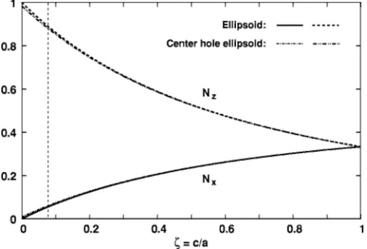
3/2 . 共24兲The main assumption, apart from the shape chosen, is that the polarization density inside this open ellipsoid has to be constant. Though this is definitely a regula falsi solution, we do not expect much deviation from the correct result for very oblate ellipsoids. The depolarization factors for both types of ellipsoid are shown in Fig. 4. The depolarization factor hardly depends on the presence of the center hole.
For the case that we want to measure the polarizability of a single dot or ring, we have to proceed differently. For the experimental situation we have to use
d =␣JEX, 共25兲 where this experimental polarizability␣ embodies also the electromagnetic self-interaction. Combining properly the two prescriptions for the induction共21兲 and 共25兲 leads to
␣
J−1=␣J G −1
− tJ. 共26兲
This is a very important relationship, showing that there should be a serious discrepancy between measured and quan-tum mechanically calculated polarizabilities.
In expression共20兲 for ␣Gwe need separately an expres-sion for ␣GS, the quantum-mechanical static polarizability tensor of the dot or ring. For the special case that we repre-sent the dot by an strongly oblate homogeneous dielectric ellipsoid with relative dielectric constant⑀, this static polar-izability is isotropic and can easily be obtained. It suffices to introduce for this ellipsoid its␣GS as
␣GS,vv=␣GS=⑀0V共⑀− 1兲 =␣0fV共⑀− 1兲, ␣0= 4⑀0aL 3 , fV= ⑀0V ␣0 = V 4aL 3, 共27兲
where we introduce the two normalization factors␣0and fV. Next we use Eq. 共26兲 to determine the measurable polariz-ability␣S: ␣S,vv= ␣GS 1 − tS,vv␣GS =⑀0V
冋
⑀− 1 1 + Nv共⑀− 1兲册
. 共28兲The same expression has been obtained along a different line of derivation by Avelin.33For arbitrary shapes of the dots and rings only a full numerical calculation can be done. The re-sult of such calculation will be ␣S,vv. In Eq. 共20兲 we need
␣GS,vvand not␣S,vv. The expression for␣GS,vvis simple and given already in Eq. 共27兲. The numerical determination of
␣S,vv is necessary to obtain the right value for tS for arbi-trarily shaped bodies from the relation
t JS=␣JGS −1 −␣JS −1 . 共29兲
This value for tS,vvdetermines the expression for the applied field in case of arbitrarily shaped bodies.
If we surround this individual dot or ring by a 共square兲 lattice of identical dots and rings, with aLas lattice spacing, the only difference is that we have to replace the external field EX by the local field EL, given for the single lattice plane by
EL= EX+ fI · d,
⬘
EA= EL+ tJ· d, 共30兲
where f
⬘
is the intraplanar transfer tensor for the plane. This transfer tensor f⬘
can be determined numerically to any pre-cision using the Ewald one-fold integral transform.15Vlieger, however, has derived, after much effort, a more concise expression:16FIG. 4. Depolarization factors Nx,z as a function of the aspect ratio=c/a for normal and center hole ellipsoid. Dashed line at = 0.081. Center hole diameter d = 0.257 a.
fJ
⬘
=␣0−1Jf⬘
S+ i 2⑀0aL 2兩k z兩 关k2J − k1 储k储T− kz2zˆ · zˆ T兴 − ik 3 6⑀0 1 J, f⬘
S,xx= f⬘
S,yy= − 4.51681, f⬘
S,zz= − 2 f⬘
S,xx= 9.03362, 共31兲 where parallel共储兲 means parallel to the plane of the dots or rings. The strong aspect of the Vlieger expression is that it gives the intraplanar transfer tensor as a dynamical correc-tion to its static counterpart. This guarantees smooth linkage to the static result, being for a square lattice essentially only the numbers given above. The induction for a dot or ring inside a lattice now becomesd =␣JG关EX+共fJ
⬘
+ tJ兲d兴, 共fJ⬘
+ tJ兲 =␣0−1共fJ⬘
S+ tJS兲 + i 2⑀0aL2兩kz兩 关k2J − k1 储k储 T − kz 2 zˆ · zˆT兴, tS,vv= −Nv共兲 fV , 共32兲where, as in the Vlieger derivation, the radiation damping term has disappeared.
D. Electromagnetic response
The electromagnetic response of the layer of dots/rings, has to be determined in two steps. The dipole strength d induced in the plane is obtained from
d =关1J −␣JG共fJ
⬘
+ tJ兲兴−1␣JGEX. 共33兲 The reflected electric fields at a remote site R are now given by ER共R兲 = fJRd, f JR= i k2eik·R 2⑀0aL2kz 关1J − kˆ · kˆT兴, k = k储− kzzˆ, 共34兲 where fRis the remote interplanar transfer tensor. Physically only those electric fields make sense which go in a direction away from the sources. This means that when the sign ofis changed also the corresponding wave number or wave vector has to change sign. Therefore it is easily seen that in the above expression when is replaced by −, both k and kz have to change sign. Therefore all transfer tensors t, f⬘
, and fR will always turn into their complex conjugate when changes sign. We have shown already in detail that the same behavior applies also to ␣G.23 This mathematical property guarantees that the dipole strength induced in the plane and the electric field emitted by the plane of dots and rings will be real according toE共r,t兲 = Re关fJR共兲d共兲e−it兴. 共35兲 This elementary result and Eqs.共33兲 and 共34兲 allow the en-tire electromagnetic derivation to be done using a single complex exponential. Also the following relationship is use-ful, if not indispensable:
具AB典 =1 T
冕
0 T dt A共t兲B共t兲 =1 T冕
0 TdtRe关A˜0e−it兴Re关B˜0e−it兴 = 1 2Re关A˜0 * B ˜ 0兴 共36兲
for any two harmonic fields A共t兲, B共t兲 and further T = 2. For electromagnetic derivations, different from the quantum-mechanical derivations treated in Ref. 23, the complex nota-tion is only auxiliary in character and allows for the common smooth usage.
In a further straightforward manner it is easy to show now that only the following reflection and transmission coeffi-cients suffice to describe the full electromagnetic response of a square plane of dots and rings:
rss= fk Aycosi− fk , rpp= fkcosi Ax− fkcosi − fksin 2 i Azcosi− fksin2i , tss − = 1 + rss, tpp − = fkcosi Ax− fkcosi − Azcosi Azcosi− fksin2i , 共37兲
whereiis the angle of incidence. Further use has been made of the notation t− for the transmission coefficient to distin-guish it from the self-interaction t and of the following ab-breviations to make the expressions more concise:
Av=␣0␣G,vv−1 −共fS,vv
⬘
+ tS,vv兲,fk= 2iaLk 共38兲 withv as defined before. These reflection coefficients are not directly measurable as they are. Measurable are only the re-flectances Rqqand transmittances Tqqdefined as
Rqq= rqq* rqq, Tqq= tqq −* tqq − , 共39兲
where q stands for the ellipsometric directions s, p. From the energy balance point of view these quantities determine the absorbance Aqqin the lattice plane according to
Aqq= 1 − Rqq− Tqq= 0c aL 2 EX 2 cosi lm共EA*Td兲,
where EX is the amplitude of the externally incoming plane wave. Measurable, but less directly, are also the ellipsometric angles⌿, ⌬, which follow from the commonly used defini-tion:
r= rpp rss
= tan⌿ ei⌬
In the next section these experimentally accessible quantities will be calculated numerically for the plane of dots and rings.
III. NUMERICAL RESULTS
Using the above expressions for reflection coefficients and related ellipsometric angles⌿, ⌬, we have determined the optical response of a square lattice made from nanorings and, for comparison, from quantum dots. All relevant input material has been collected in Table I.
The optical response for individual dots and rings is com-pletely controlled by the polarizability␣G, given by Eq.共20兲. The static part of it,␣GS, is given by Eq. 共27兲 and is com-pletely determined by the volume V. Volume V is given for the ellipsoid by Eq.共23兲 and for the center hole ellipsoid by Eq. 共24兲. The geometrical data determining these ellipsoids 共see Fig. 1兲 are a, c, and d and have the values given in Table I. The aspect ratiofor both ellipsoids and center hole ellip-soids then becomes
= c/a = 0.081
and the corresponding depolarization factors Nz, Nx are for the ellipsoids共dots兲:
Nz= 0.8848, Nx= 0.0576 and for the center hole ellipsoids共rings兲
Nz= 0.8757, Nx= 0.0622.
The volume of the ellipsoid共dot兲 is V=2.125⫻10−24m3and for the center hole ellipsoid共ring兲 V=1.917⫻10−24m3. To calculate the static polarizability␣GS we need the value of the dielectric constant⑀ for 共InAs兲, the material making up the dot or ring and given in Table I. That number belongs to high-frequency共IR兲 data at room temperature, since we con-sider that to be the best choice.
For an single isolated dot or ring, using Eq.共28兲, we find the following tensor components␣GS and␣vvfor dots:
␣GS= 3.711⫻ 10−3␣0,
␣S,xx= 2.256⫻ 10−3␣0,
␣S,zz= 3.401⫻ 10−4␣0, and correspondingly for rings
␣GS= 3.348⫻ 10−3␣0,
␣S,xx= 2.188⫻ 10−3␣0,
␣S,zz= 3.434⫻ 10−4␣0,
where␣0= 5.69677⫻10−32F m2. The anisotropy of the static polarizability␣S is entirely due to the electromagnetic self-interaction of the dot or ring. Quantum mechanics plays no role in it.
This will change for frequencies near the energy gap of the dot or ring. Then there is a strong quantum-mechanical contribution to the anisotropy. To determine numerically the dynamic quantum-mechanical part of the polarizability ␣G requires knowledge of the overlap matrix elements具Fhl兩Fcl典. Those were obtained numerically by solving the effective mass Hamiltonian共13兲 with the Ben Daniel-Duke boundary condition共14兲. The resulting values are in Table I . There is also the bulk optical matrix element rch. The transition fre-quencieslkare shown in Fig. 3, but the damping␥can only be used as a free parameter. We have used two values 2 meV and 5 meV for it. If we takeប= 0.86 eV as a typical energy for the interband transitions of the dots or rings, this corre-sponds to a wavelength=1459 nm, well beyond the lattice spacing aL. This ensures that the Vlieger expressions can be used as they are and that we do not have to bother about possible higher order reflections.
The ellipsometric angles⌿ and ⌬ are shown for this con-figuration in Figs. 5 and 6. They are shown in each figure for dots at the left and for rings at the right. The upper panels show results for ␥= 2 meV and the lower panels for ␥ = 5 meV. The crucial difference between dots and rings is in the crossing of energy levels. For dots there are no crossings for varying magnetic field strength B, opposite to the behav-ior of the rings. So the ⌿ data display quite monotonous ridgelike patterns for dots but a clear “hill/valley” pattern for rings. This represents a typical manifestation of the optical Aharonov-Bohm effect. This more remarked dependence of the rings upon changes in the magnetic field strength gives them better characteristics for practical use than dots.
This behavior becomes even more manifest for the other ellipsometric angle⌬ as shown in Fig. 6. In degrees the peak to peak values for ⌬ are about five times larger than the corresponding variation in ⌿. Rings in general respond stronger for both angles than dots. This is remarkable, since the volume fraction fVis smaller for rings than for dots. Yet the understanding of this behavior is quite down to earth: the crossings cause two pairs to contribute in resonance simulta-neously and this effectively doubles the response. All values drop by about the same factor as the damping␥is increased for all cases. This is due and in agreement with the general behavior of the frequency dependent functions flk共兲, as given by Eq.共1兲. All values for ⌿ and ⌬ have variations of the order of magnitude of degrees and are therefore easily TABLE I. Basic input parameters for lattices of dots and rings.
For the meaning of the symbols, see text.
Quantum dot Nanoring
aL 80.0 nm 80.0 nm a 18.45 nm 18.45 nm c 1.49 nm 1.49 nm d 0.00 nm 4.75 nm 兩具Fh0兩Fc0典V兩 0.9454 0.9 兩具Fh,−1兩Fc,−1典V兩 0.9285 0.9 兩具Fh,−2兩Fc,−2典V兩 0.9120 0.9 rch 0.60 nm 0.60 nm ⑀ 12.2 12.2 EG共T=0°K兲 0.42 eV 0.42 eV
within range of any modern ellipsometer. Yet it should be mentioned that the variations in⌿, ⌬ will reduce drastically, when the embedding is taken into account also, as we hope to show in a forthcoming publication.
The ellipsometric parameters⌿, ⌬ are relative quantities and do not contain knowledge about the absolute values of optical response coefficients. Therefore also reflectance and absorbance have been determined for a case where both the ring and the dot lattice have a maximum in the imaginary part of their polarizability共resonance兲. For both systems we chose a magnetic field strength of B = 7 T and a damping of ប␥= 5 meV. The selected resonance frequencies were ប = 0.867 eV for the dot andប= 0.854 eV for the ring lattice. The reflectance for those settings is shown in Fig. 7. Typi-cally the values are in the 10−5 range, so pretty weak. The ring lattice has a slightly weaker reflectance than the dot lattice, but both systems display the usual angular dependent behavior. The most outspoken aspect is the occurrence for p polarization of the Brewster minimum at about 68°. For bulk InAs the Brewster angle has the value of 74° for comparison. By means of Eq.共40兲 we have also calculated the absor-bance. This quantity has the most direct connection to the detailed treatment of the microscopic behavior given in this
paper, both electromagnetically and quantum mechanically. The results are shown in Fig. 8. The overall picture is that the absorbance in the ring system is stronger than for the dot system. This is the consequence of the enlargement at reso-nance of the imaginary part of the polarizability due to the crossing of energy levels in the ring system. Indeed the en-largement is about a factor of 2. The most remarkable aspect of the absorbance is the strongly increased dichroism for increasing angles of incidence. For the hypothetical case that the dots or rings would have had an isotropic polarizability, both polarization directions s and p would behave similar to the s components in Fig. 8 . Although the anisotropic behav-ior of the polarizability of the elements goes back both to electromagnetism 共through the electromagnetic self-tensor兲 and to quantum mechanics共through the expectation value of the position vector兲, the dichroism is governed in the first place by quantum mechanics. For light components in the z direction the dots and rings will be transparent, for the re-maining x, y direction they will be absorbing. So it looks as if research concerning the shape and volume independence of the optical response for isolated levels at resonance, should focus upon absorbance and the dichroism found here. FIG. 5. Ellipsometric angle⌿ for a monolayer of InAs quantum dots and nanorings. 共a兲,共b兲 ⌿ for i= 60° andប␥=2 meV. 共c兲,共d兲 ⌿
fori= 60° andប␥=5 meV. Left panels 共a兲,共c兲: dots, right panels 共b兲,共d兲: rings.
IV. SUMMARY AND CONCLUSIONS
In this paper we have performed a comparative study of the optical response functions共such as reflectance and absor-bance and the ellipsometric angles⌿, ⌬兲 for quantum dots
and nanorings, when they are arranged in a square lattice. We have developed accurate and workable expressions for the response terms of separate quantum dots and nanorings as given by the polarizability. The polarizability is determined FIG. 6. Ellipsometric angles⌬ for a monolayer of InAs quantum dots and nanorings. 共a兲,共b兲 ⌬ for i= 60° andប␥=2 meV. 共c兲,共d兲 ⌬
for i= 60° and ប␥=5 meV. Left
panels 共a兲,共c兲: dots, right panels 共b兲,共d兲: rings.
FIG. 7. Reflectance R for a monolayer of InAs quantum dots and nanorings. B = 7 T. Dots:ប=0.867 eV, rings: ប=0.854 eV. Both:ប␥=5 meV.
FIG. 8. Absorbance A for a monolayer of InAs quantum dots and nanorings. B = 7 T. Dots:ប=0.867 eV, rings: ប=0.854 eV. Both:ប␥=5 meV.
by both quantum-mechanical and electromagnetic interac-tions. For nano-objects an outspoken consequence of these two aspects of the polarizability is that far below the energy gap the strength of the polarizability is volume and shape dependent, whereas for separately observable resonant tran-sitions at the absorption edge the strength is volume and shape independent. For the optical response of the square lattices made up from these nano-objects only the electro-magnetic interaction needs to be taken into account. The re-mote response, as represented by reflection and transmission coefficients has been obtained by remote propagators as usual in discrete optics and these coeficients build a key in-strument for the quantitative analysis of the magneto-optical response of lattices made from nanosized objects. The calcu-lations clearly show that rings are more effective to exploit the dependence from magnetic fields than dots. Despite a lower volume fraction rings have stronger variation in any of the ellipsometric angles than the dots. The crossing of the transition energies, being characteristic for rings and known as the optical Aharonov-Bohm effect, results in a pronounced
variation of the ellipsometric angles for varying magnetic field. The reflectances for both types of lattice are weak, as can be expected from such thin layerlike systems. Remark-able is the strongly increasing dichroism for increasing angles of incidence. Since the origin of this dichroism is in the dynamic part of the anisotropy of the polarizability of the nano-objects, this dichroism can be of use to investigate the size- and shape-dependent behavior of the polarizability. The theoretical findings obtained here, yield also the essential starting point for future work to incorporate the influence of the embedding 共capped quantum-dot or nanoring systems兲. This comparative study shows that use of nano-rings or quantum dots in both the investigation and use of magneto-optical response is in favor of the first.
ACKNOWLEDGMENTS
This work was funded by the National Science Council of Taiwan under Contracts No. NSC-93-2215-E-009-006 and NSC-93-2112-M-009-008.
1J. D. Joannopoulos, R. D. Meade, and J. N. Winn, Photonic
Crys-tals: Molding the Flow of Light 共Princeton University Press,
Princeton, 1995兲.
2V. G. Veselago, Sov. Phys. Usp. 10, 509共1968兲.
3J. B. Pendry, A. J. Holden D. J. Robbins, and W. J. Stewart, IEEE
Trans. Microwave Theory Tech. 47, 2075共1999兲.
4O. Voskoboynikov, Yiming. Li, Hsiao-Mei Lu, Cheng-Feng Shih,
and C. P. Lee, Phys. Rev. B 66, 155306共2002兲; O. Voskoboyni-kov and C. P. Lee, Physica E共Amsterdam兲 20, 278 共2004兲.
5D. Bimberg, M. Grundmann, and N. N. Ledentsov, Quantum Dot
Heterostructures共Wiley Interscience, New York, 1998兲.
6J. M. Garcia, G. Medeiros-Ribeiro, K. Schmidt, T. Ngo, J. L.
Feng, A. Lorke, J. Kotthaus, and P. M. Petroff, Appl. Phys. Lett.
71, 2014共1997兲 .
7Y. Aharonov and D. Bohm, Phys. Rev. 115, 485共1959兲. 8A. O. Govorov, S. E. Ulloa, K. Karrai, and R. J. Warburton, Phys.
Rev. B 66, 081309共R兲 共2002兲.
9J. I. Climente, J. Planelles, and W Jaskolski, Phys. Rev. B 68,
075307共2003兲; J. Climente, J. Planelles, W. Jaskolski, and J. I. Aliaga, J. Phys.: Condens. Matter 15, 3593共2003兲.
10A. Lorke and R. J. Luyken, Physica B 256-B258, 424共1998兲; A.
Lorke, R. J. Luyken, A. O. Govorov, J. P. Kotthaus, J. M. Gar-cia, and P. M. Petroff, Phys. Rev. Lett. 84, 2223共2000兲.
11J. Planelles, W. Jaskolski, and J. I. Aliaga, Phys. Rev. B 65,
033306共2001兲.
12M. Bayer, M. Korkusinski, P. Hawrylak, T. Gutbrod, M. Michel,
and A. Forchel, Phys. Rev. Lett. 90, 186801共2003兲.
13H. Pettersson, R. J. Warburton, A. Lorke, K. Karrai, J. P.
Kot-thaus, J. M. Garcia, and P. M. Petroff, Physica E共Amsterdam兲
6, 510共2000兲.
14G. Y. Slepyan, S. A. Maksimenko, V. P. Kalosha, A. Hoffmann,
and D. Bimberg, Phys. Rev. B 64, 125326共2001兲.
15G. P. M. Poppe, C. M. J. Wijers and A. van Silfhout, Phys. Rev.
B 44, 7917共1991兲.
16J. Vlieger, Physica共Amsterdam兲 64, 63 共1973兲; C. M. J. Wijers
and K. M. E. Emmett, Phys. Scr. 38, 435共1988兲.
17B. C. Lee, O. Voskoboynikov, and C. P. Lee, Physica E
共Amster-dam兲 24, 87 共2004兲.
18X. Z. Liao, J. Zou, X. F. Duan, D. J. H. Cockayne, R. Leon, and
C. Lobo, Phys. Rev. B 58, R4235共1998兲
19H. A. Kramers and W. Heisenberg, Z. Phys. 31, 681共1925兲. 20O. S. Stier, M. G. Grundmann, and D. B. Bimberg, Phys. Rev. B
59, 5688共1999兲.
21G. W. Bryant, Phys. Rev. B 37, 8763共1988兲.
22P. Enders, A. Bärwolff, M. Woerner, and D. Suisky, Phys. Rev. B
51, 16 695共1995兲.
23C. M. J. Wijers, Phys. Rev. A 70, 063807共2004兲.
24H. E. van den Brom and J. M. van Ruitenbeek, Phys. Rev. Lett.
82, 1526共1999兲.
25G. Bastard, Wave Mechanics Applied to Semiconductor
Hetero-structures共Les Edition de Physique, Les Ulis, 1990兲.
26J. I. Climente, J. Planelles, and J. L. Movilla, Phys. Rev. B 70,
081301共R兲 共2004兲.
27E. O. Kane, J. Phys. Chem. Solids 1, 249共1957兲.
28M. Asada, A. Kameyama, and Y. Suematsu, IEEE J. Quantum
Electron. 20, 745共1984兲; M. Asada and Y. Suematsu, ibid. 21, 434共1985兲; M. Asada, Y. Miyamoto, and Y. Suematsu, ibid. 22, 1915共1986兲.
29L. V. Asryan and R. A. Suris, Semicond. Sci. Technol. 11, 554
共1996兲.
30S. L. Chuang, Physics of Optoelectronic Devices 共Wiley, New
York, 1995兲.
31P. G. Eliseev, H. Li, A. Stintz, G. T. Liu, T. C. Newell, K. J.
Malloy, and L. F. Lester, Appl. Phys. Lett. 77, 262共2000兲.
32V. Belevitch and J. Boersma, Philips J. Res. 38, 79共1983兲. 33J. Avelin, Ph.D. thesis, Electromagnetics Laboratory, Helsinki