This content has been downloaded from IOPscience. Please scroll down to see the full text.
Download details:
IP Address: 140.113.38.11
This content was downloaded on 25/04/2014 at 04:19
Please note that terms and conditions apply.
Asymmetric gate capacitance and dynamic characteristic fluctuations in 16 nm bulk
MOSFETs due to random distribution of discrete dopants
View the table of contents for this issue, or go to the journal homepage for more 2010 Semicond. Sci. Technol. 25 045006
(http://iopscience.iop.org/0268-1242/25/4/045006)
Semicond. Sci. Technol. 25 (2010) 045006 (8pp) doi:10.1088/0268-1242/25/4/045006
Asymmetric gate capacitance and
dynamic characteristic fluctuations in
16 nm bulk MOSFETs due to random
distribution of discrete dopants
Kuo-Fu Lee
1, Yiming Li
1,2,3and Chih-Hong Hwang
11Department of Electrical Engineering and Institute of Communications Engineering, National Chiao-Tung University, Hsinchu 300, Taiwan
2National Nano Device Laboratories, Hsinchu 300, Taiwan E-mail:[email protected]
Received 10 October 2009, in final form 22 January 2010 Published 23 February 2010
Online atstacks.iop.org/SST/25/045006
Abstract
Characteristic variability of a transistor is a crucial issue for nanoscale
metal-oxide-semiconductor field-effect transistors (MOSFETs). In this study, we explore the asymmetric sketch of the random dopant distribution near the source end and the drain end in 16 nm MOSFETs. Discrete dopants near the source and drain ends of the channel region induce rather different fluctuations in gate capacitance and dynamic characteristics. Based upon the observed asymmetry properties, a lateral asymmetry channel doping profile
engineering is then proposed to suppress the random-dopant-induced characteristic fluctuations in the examined devices and circuits. The results of this study indicate that the fluctuations in average gate capacitance, circuit gain, 3 db bandwidth and unity-gain bandwidth for the cases with dopants near the drain side could be simultaneously reduced by 62.6%, 22.2%, 63.1% and 41.4%, respectively. Consequently, such a lateral asymmetry channel doping profile could be considered to design intrinsic parameter fluctuation resistant transistors.
(Some figures in this article are in colour only in the electronic version)
1. Introduction
The gate lengths of scaled metal-oxide-semiconductor field-effect transistors (MOSFETs) have been the sub-30 nm for
45 nm node high-performance circuit design [1]. Moreover,
the devices with sub-10 nm gate lengths have been currently
investigated [2–5]. For the radio-frequency/mixed-signal
applications, a cutoff frequency higher than 200 GHz has
been also reported [6, 7]. Yield analysis and optimization,
which take into account the manufacturing tolerances, model uncertainties, variations in the process parameters, etc, are known as indispensable components of the circuit design
methodology [8–12].
As geometries of MOSFET shrink, the intrinsic device
parameter variations such as line edge roughness [13], the
3 Author to whom any correspondence should be addressed.
granularity of the polysilicon gate [14,15], random
discrete-dopant effects [16–32] have brought significant impacts on
device characteristic fluctuations; it is imperative to model and mitigate them in silicon technology. Furthermore, various randomness effects resulting from the random nature of manufacturing process, such as ion implantation, diffusion and thermal annealing, have induced significant fluctuations in the electrical characteristics in nanometer scale (nanoscale)
MOSFETs. The number of dopants is of the order of
tens in the depletion region of a nanoscale MOSFET whose influence on device characteristic is large enough to be distinct
[16]. Various random dopant effects have been recently
studied in both experimental and theoretical approaches
[16–32]. Fluctuations in characteristics are caused not only by
a variation in an average doping density, which is associated with a fluctuation in the number of impurities, but also with
Semicond. Sci. Technol. 25 (2010) 045006 K-F Lee et al
a particular random distribution of impurities in the channel
region. Diverse approaches have recently been reported
to study fluctuation-related issues in semiconductor devices
[16–30] and a digital integrated circuit [31–35]. So far, the
attention is mostly drawn on the fluctuations in threshold
voltage and dc characteristics. However, the investigation
of intrinsic fluctuation in gate capacitance and dynamic characteristics due to random dopant placement is still not clear.
In this study, a large-scale 3D ‘atomistic’ device-circuit-coupled simulation is performed on a parallel computing
system [36–41] to analyze the discrete-dopant-induced gate
capacitance and dynamic characteristic fluctuations for the
tested 16 nm MOSFET and circuit. Based upon the
asymmetric sketch of the random dopant distribution near the source end and the drain end, it is found that discrete dopants near the source and drain ends of a channel region induce rather different fluctuations in gate
capacitance and dynamic characteristics. This asymmetry
property is utilized to design a lateral asymmetry channel doping profile for the reduction of random-dopant-induced
characteristic fluctuations. Consequently, fluctuations in
average gate capacitance, circuit gain, 3 db bandwidth and unity-gain bandwidth for the cases with dopants near the drain side are reduced by 62.6%, 22.2%, 63.1% and 41.4%, respectively. The lateral asymmetry channel doping profile could be considered to design intrinsic parameter
fluctuation resistant transistors. Notably, the statistically
sound analyzing methodology was quantitatively verified with
the experimentally measured data of 20 nm CMOS [22–26]
for the best accuracy.
The paper is organized as follows. In section2, we brief
the analyzing technique for studying the random dopant effect
in a nanoscale device and circuit. In section3, we examine
the discrete-dopant-induced characteristic fluctuations in the
16 nm MOSFET devices and circuits. Finally, we draw
conclusions and suggest future work.
2. The computational procedure
The original channel doping concentration of a device is
1.48 × 1018 cm−3. It has a 16 nm gate, a silicon oxide
gate thickness of 1.2 nm and a mid-gap metal gate with a workfunction of 4.4 eV. The generation approach for
discrete-dopant cases follows our previous work [21–27]. Outside
the channel, the doping concentrations in the source/drain
and background in silicon are 1.1 × 1020 cm−3 and 1 ×
1015cm−3, respectively. Inside the channel region, to consider
the effect of random fluctuation in discrete channel dopants,
758 dopants are first randomly generated in an (80 nm)3
cube, in which the equivalent doping concentration is 1.48×
1018 cm−3, as shown in figures 1(a)–(d). The generation
of a dopant distribution is totally randomly from computer
simulation program. This completely randomized dopant
generation of three dimensions can ensure the nominal doping
concentration to be 1.48 × 1018 cm−3 (=758 dopants/
(80 nm)3). Then the (80 nm)3cube is partitioned into 125
sub-cubes of (16 nm)3, where the dopants may vary from 0 to 14
(the average number= 6) within its sub-cubes. We define the
channel doping profile in the (16 nm)3cube only, as shown in
the cube of figure1(b). For the channel dopant distribution
outside the (16 nm)3sub-cube, definitely, the channel dopants
will appear outside the defined (16 nm)3sub-cube. However,
since the operation of MOSFET is through surface conduction, the influence of such channel dopants should be not significant
in random dopant fluctuation. These sub-cubes are then
equivalently mapped into the three-dimensional (3D) device
channel region, shown in figure1(e). All statistically generated
discrete dopants are incorporated into the large-scale 3D
‘atomistic’ simulation under parallel computing system [39].
The quantum mechanically corrected transport simulation is performed by solving a set of 3D density-gradient equation
coupling with drift-diffusion equations. Figure1(f ) shows the
tested circuit for exploring the discrete-dopant-fluctuated high-frequency characteristics. To properly estimate the discrete-dopant-fluctuated high-frequency characteristics, due to lack of a well-known compact model of 16 nm MOSFET for circuit simulation, a 3D device- and circuit-coupled simulation with discrete dopants is conducted. Notably, only channel dopants
are treated discretely: the doping concentrations remain
continuous in the source/drain region because the volume of source/drain dopants is significantly larger than that of channel
region [26]. This approach allows us to focus on the study
of characteristic fluctuations induced by the random-dopant number and position in the channel simultaneously.
As for the generation of lateral asymmetry doping, the adapted near-drain-end and near-source-end channel doping
profiles are shown in figure 1(g). Only half of the channel
is doped and 758 dopants are randomly generated in a large rectangular solid (gate width, source–drain direction, channel
depth: 40 nm× 80 nm × 80 nm). Therefore, the effective
channel doping concentration is still 1.48× 1018cm−3. Then
the large cube is partitioned into 125 sub-cubes ((8 nm) ×
(16 nm)× (16 nm)) and mapped into the drain end of a channel
region for discrete-dopant simulation. Similarly, the dopants in sub-cubes may vary from 0 to 14 (the average number is 6)
within its sub-cubes, as shown in figure1(h). To estimate the
device characteristics on the same basis, the threshold voltage for both the original MOSFETs and the asymmetric MOSFETs are calibrated.
3. Results and discussion
In this section, the discrete-dopant-induced threshold voltage
(Vth), gate capacitance (Cg) and high-frequency circuit
characteristics fluctuations are first analyzed. Then 500
discrete-dopant-fluctuated transistors are classified into the cases of the near-source end and near-drain end for the studying of the asymmetry sketch of characteristics fluctuations. Then a lateral asymmetry doping profile is implemented to examine the associated fluctuation suppression technique.
3.1. Asymmetric device characteristic fluctuations
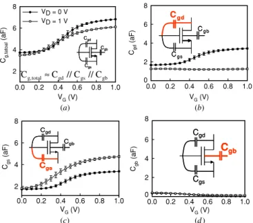
Figure2(a) shows the total gate capacitance (Cg ,total) versus
the drain bias (VD) for all discrete-dopant-fluctuated devices,
Dopants in (16nm3) Cube 0 5 10 15 Histog ram ( n umber) 0 5 10 15 20 25 -3σ +3σ 0 14 Mean = 6 80nm 8 0 n m 1.48×1018cm-3 758 dopants in 80 nm3cube 80nm (a) Dopants in (16nm3) Cube 0 5 10 15 Histog ram ( n umber) 0 5 10 15 20 25 -3σ +3σ 0 14 Mean = 6 80nm 8 0 n m 1.48×1018cm-3 758 dopants in 80 nm3cube 80nm 14 dopants in 16 nm3cube 16nm 16nm 16nm 1 6 n m 1 6 n m zero dopants in 16 nm3cube 14 dopants in 16 nm3cube 16nm 16nm 16nm 16nm 1 6 n m 1 6 n m zero dopants in 16 nm3cube (a) VDD Vgate Planar MOSFETs Vsource Vdrain C R2 R1 oxide Channel Length Gate drain source VDD Vgate Planar MOSFETs Vsource Vdrain C R2 R1 oxide Channel Length Gate drain source (e) (f ) NA= 2.96×1018cm-3 undoped Source Source Drain Conventional LAC device Inverse LAC device Dopants in (16x16x8)nm3 cube 0 5 10 15 His to gr a m ( n u m be r) 0 5 10 15 20 25 Dopants in (16x16x8)nm3 cube 0 5 10 15 Hi st o g ra m ( n u m b e r) 0 5 10 15 20 25 30 Conventional LAC device Inverse LAC device Drain (g) (h) Dopants in (16nm3) Cube 0 5 10 15 Histog ram ( n umber) 0 5 10 15 20 25 -3σ +3σ 0 14 Mean = 6 Dopants in (16nm3) Cube 0 5 10 15 Histog ram ( n umber) 0 5 10 15 20 25 -3σ +3σ 0 14 Mean = 6 80nm 8 0 n m 1.48×1018cm-3 758 dopants in 80 nm3cube 80nm (a) Dopants in (16nm3) Cube 0 5 10 15 Histog ram ( n umber) 0 5 10 15 20 25 -3σ +3σ 0 14 Mean = 6 Dopants in (16nm3) Cube 0 5 10 15 Histog ram ( n umber) 0 5 10 15 20 25 -3σ +3σ 0 14 Mean = 6 80nm 8 0 n m 1.48×1018cm-3 758 dopants in 80 nm3cube 80nm 14 dopants in 16 nm3cube 16nm 16nm 16nm 1 6 n m 1 6 n m zero dopants in 16 nm3cube 14 dopants in 16 nm3cube 16nm 16nm 16nm 16nm 1 6 n m 1 6 n m zero dopants in 16 nm3cube 14 dopants in 16 nm3cube 16nm 16nm 16nm 1 6 n m 1 6 n m zero dopants in 16 nm3cube 14 dopants in 16 nm3cube 16nm 16nm 16nm 16nm 1 6 n m 1 6 n m zero dopants in 16 nm3cube VDD Vgate Planar MOSFETs Vsource Vdrain C R2 R1 oxide Channel Length Gate drain source VDD Vgate Planar MOSFETs Vsource Vdrain C R2 R1 oxide Channel Length Gate drain source NA= 2.96×1018cm-3 undoped Source Source Drain Conventional LAC device Inverse LAC device Dopants in (16x16x8)nm3 cube 0 5 10 15 H ist og ra m ( n um be r) 0 5 10 15 20 25 Dopants in (16x16x8)nm3 cube 0 5 10 15 Hi st o g ra m ( n u m b e r) 0 5 10 15 20 25 30 Conventional LAC device Inverse LAC device Dopants in (16x16x8)nm3 cube 0 5 10 15 H ist og ra m ( n um be r) 0 5 10 15 20 25 Dopants in (16x16x8)nm3 cube 0 5 10 15 Hi st o g ra m ( n u m b e r) 0 5 10 15 20 25 30 Conventional LAC device Inverse LAC device Drain (b) (c) (d)
Figure 1.(a) Discrete dopants randomly distributed in the (80 nm)3cube with the average concentration of 1.48× 1018cm−3. There will be 758 dopants within the cube, but dopants may vary from 0 to 14 within its 125 sub-cubes of (16 nm)3, ((b)–(d)). The sub-cubes are equivalently mapped into the channel region for device and device-circuit-coupled simulation as shown in (e) and (f ). The doping profile and distribution of discrete dopants for the LAC and inLAC structures are illustrated in (g) and (h).
VG (V) 0.0 0.2 0.4 0.6 0.8 1.0 Cgd (aF) 0 2 4 6 8 VG (V) 0.0 0.2 0.4 0.6 0.8 1.0 Cg,t a toa l (aF) 2 4 6 8 VD = 0 V VD = 1 V gb gs gd total g, C // C // C C ≈ Cgd Cgs Cgb Cgd Cgs Cgb Cgd Cgs Cgb Cgd Cgs Cgb (a) (b) (c) (d ) VG (V) 0.0 0.2 0.4 0.6 0.8 1.0 Cgb (a F) 0 2 4 6 8 VG (V) 0.0 0.2 0.4 0.6 0.8 1.0 Cgs (aF) 2 4 6 8 Cgd Cgs Cgb Cgd Cgs Cgb Cgd Cgs Cgb Cgd Cgs Cgb
Figure 2.(a) The total gate capacitance (Cg ,total= Cgd// Cgs// Cgb), where aF= 10−18F; (b) gate-drain capacitance (Cgd); (c)
gate-source capacitance (Cgs); (d) gate-bulk capacitance (Cgb) of all discrete-dopant-fluctuated 16 nm-gate planar MOSFETs, where the symbol and error bar denote the characteristics of normal case and fluctuation, respectively.
where the symbol and error bar denote the characteristics
of normal case and fluctuation, respectively. Cg ,total results
from the shunt of the gate-drain capacitance (Cgd), the
gate-source capacitance (Cgs) and the gate-bulk capacitance (Cgb).
Figures2(b)–(d) show the components of Cgd, Cgs and Cgb;
as VDchanges from 0 V (open circles) to 1 V (fill-in circles),
Cgdand the fluctuation of Cgd(σ Cgd) are decreased due to the
widerness of the depletion layer near the drain junction and the
effect of channel pinch-off, as displayed in figure2(b). Then
Cgs and its fluctuation are increased, as shown in figure2(c).
As for Cgb, the fluctuation is small enough to be neglected,
Group 1: near source end ( dopant located near drain 1)
Selection Criterion
source drain
source drain
(a)
Group 2: near drain end
( dopant located near source 1)
source drain
source drain
(b)
Figure 3.The discrete-dopant-fluctuated devices are then classified into two groups: (a) devices with dopants near the source end and (b) devices with dopants near the drain end.
as shown in figure 2(d). The drain bias-induced different
variations in Cgdand Cgsare observed, and the dependence of
Cgon different VDmotivates the design of a lateral asymmetry
doping profile along the source-drain direction.
We generate 500 discrete-dopant-fluctuated transistors
exploiting similar approach, as shown in figures 1(a)–(e),
and classify them into two groups according to the random distribution of discrete dopants: the cases of dopants near the
source end and the drain end, as shown in figure3, where
the inset describes the selection criteria. To strengthen and make the phenomenon clear, the difference between dopant numbers near the source end and the drain end must be larger than 2. There are 105 and 122 cases correspond to the cases of
Semicond. Sci. Technol. 25 (2010) 045006 K-F Lee et al VG (V) 0.0 0.2 0.4 0.6 0.8 1.0 Ave rag ed Cg, tat a l (aF ) 3.5 4.0 4.5 5.0 5.5 6.0 6.5 7.0
Dopant near source-end Dopant near drain-end
VD= 0 V VG (V) 0.0 0.2 0.4 0.6 0.8 1.0 Ave rag ed Cg, tat a l (aF ) 3.5 4.0 4.5 5.0 5.5 6.0 6.5 7.0
Dopant near source-end Dopant near drain-end
VD= 0 V (a) (b) VG (V) 0.0 0.2 0.4 0.6 0.8 1.0 Avera ged Cg,tatal (aF) 3.0 3.5 4.0 4.5 5.0 5.5 6.0 6.5
Dopant near source-end Dopant near drain-end
Figure 4.(a) Average of total gate capacitance (Cg ,total) at (a) VD=
0 V and (b) VD= 1 V.
dopants near the source end and the drain end. For the cases of the near-source end, the selection criterion is that a device has more than three dopants in the near-source-end channel but with zero or one dopant locating near the other end. The cases of the near-drain end are then selected accordingly. The effects of discrete dopants near the source end and the drain end on fluctuations in gate capacitances and high-frequency
characteristics are then examined. For the devices with
VD = 0 V, figure 4(a) presents the average total gate
capacitance versus the gate bias for the discrete dopants near the source end and the drain end, respectively. Both the cases of dopants near the source end and the drain end exhibit a quite
similar C–V characteristics under VD = 0 V and VD= 1 V, as
shown in figure4(b). Though the total C–V characteristics of
the two groups are very similar, the fluctuation in the total C–V
curves is outright different, as shown in figures5(a) and (b).
For devices with VD = 0 V, as shown in figure5(a), both the
cases of dopants near the source end and the drain end exhibit resembling characteristic fluctuation. However, for devices at
the bias of VD = 1 V, as shown in figure5(b), σ Cg ,totalof the
cases of dopants near the source end show a significantly large fluctuation, compared with the cases of dopants near the drain
end. Therefore, the corresponding σ Cgd and σ Cgs of devices
with VD = 0 V and 1 V are further calculated. σ Cgd and
σ Cgsof devices with VD = 0 V, as shown in figure6, indicate
that σ Cgsis more pronounced and becomes a major source of
fluctuation for the devices with the cases of dopants near the
source end. Similarly, σ Cgddominates the fluctuation in gate
capacitance for the devices with the cases of dopants near the drain end. The random dopants located near the source end or
VG (V) 0.0 0.2 0.4 0.6 0.8 1.0 Cg,total F luctu atio n ( a F) 0.00 0.05 0.10 0.15 0.20 0.25
Dopant near source-end
Dopant near drain-end VD= 0 V
(a) (b) VG (V) 0.0 0.2 0.4 0.6 0.8 1.0 Cg, total Fl uctu atio n ( a F) 0.00 0.05 0.10 0.15 0.20 0.25 VD= 1 V
Figure 5.Fluctuations of total gate capacitance at (a) VD= 0 V,
(b) VD= 1 V.
the drain end in the devices’ channel exhibit different Cgdand
Cgs characteristics in spite of the same Cg ,total and σ Cg ,total.
Notably, the drain bias will induce different characteristics in
Cgdand Cgs, as discussed in figure2. The fluctuations in Cgd
and Cgsfor devices with VD= 1 V are calculated, as shown in
figure7; for a device under a strong drain bias, the fluctuation
in Cgd is significantly reduced, as shown in figure 7(a),
compared with the result of figure 6(a). In contrast, the
fluctuation in Cgs, as shown in figure 7(b), is increased, in
contrast with the result of figure6(b). We observe that the
fluctuation in Cgd is below 0.1 aF, as shown in figure 7(a).
Therefore, for the devices with the cases of dopants near the drain end, since the major source of fluctuation is contributed
by Cgd, σ Cg ,totalis well controlled. However, for the devices
with the cases of dopants near the source end, the major source
of fluctuation, that is the fluctuation in Cgs, could not be
reduced.
Besides the fluctuation of various components in gate capacitance, we further compare the discrete-dopant-induced
threshold voltage fluctuation (σ Vth) of the conventional lateral
asymmetric channel (LAC) device which has high channel
concentration near the source end [42] and the inverse lateral
asymmetric channel (inLAC) device which has high channel
concentration near the drain end, as shown in figure8. ‘x’ and
‘o’ indicate the distribution of threshold voltage versus the dopant number for the conventional LAC and inLAC devices, where the doping profiles of the conventional LAC and inLAC
devices have been illustrated in figures 1(g) and (h). The
calculation of threshold voltage here is determined from a
current criterion for the drain current larger than 10−7(W L−1)
VG (V) 0.0 0.2 0.4 0.6 0.8 1.0 Fluctuation (aF) 0.00 0.05 0.10 0.15 0.20 0.25 VG (V) 0.0 0.2 0.4 0.6 0.8 1.0
Dopant near source Dopant near drain gate-drain capacitance (Cgd) gate-source capacitance (Cgs) VD= 0 V VD= 0 V
Figure 6.Fluctuations in Cgdand Cgsat VD= 0 V. The major
sources of fluctuation in dopant-near-drain and dopant-near-source devices are contributed from Cgdand Cgs, respectively.
VG (V) 0.0 0.2 0.4 0.6 0.8 1.0 Fluctuation ( a F) 0.0 0.1 0.2 0.3
Dopant near source Dopant near drain
VG (V) 0.0 0.2 0.4 0.6 0.8 1.0 gate-drain capacitance (Cgd) gate-source capacitance (Cgs) VD= 1 V VD= 1 V
Figure 7.Fluctuations in Cgdand Cgsat VD= 1 V, where the Cgd fluctuations are well controlled.
Dopant Number 0 2 4 6 8 10 12 14 16 Vth (V) 0.0 0.1 0.2 0.3
0.4 Conventional LAC devices inverse LAC devices
Figure 8.Comparison of the σ Vthfluctuations for the LAC and inLAC structures.
A. σ Vth of the proposed inLAC device is 1.6 times smaller
than the conventional LAC device because of the smaller current variation for dopants near the drain end of channel.
Therefore, an analog circuit, as shown in figure1(f ), using
the proposed inLAC device is implemented and compared with planar MOSFETs (where the MOSFETs are with symmetric channel doping) to estimate the dynamic characteristic fluctuations. Frequency (Hz) 108 109 1010 1011 1012 Hi gh Fre q u e n cy Ci rcu it G a in (d b) 0 2 4 6 8
10 Dopant near source
Dopant near drain Circuit gain fluctuation Unity-gain bandwidth fluctuation 3db bandwidth fluctuation
Figure 9.High-frequency response of the studied devices. The solid lines are due to the results of devices with random dopants near the source side and the dash lines are due to the results near the drain side.
Table 1.DC and high-frequency characteristic fluctuations for devices with the original doping profile.
Vth(mV) Ion(A) Ioff(A) gm,max(S)
58.5 6.7× 10⁻⁷ 9.5× 10⁻⁹ 2.1× 10⁻⁷ Cg(×10−3fF) Gain (dB) 3dB bandwidth Unity-gain
(Hz) bandwidth (Hz)
0.24 0.465 9.63 x10⁹ 2.93× 10¹⁰
3.2. Dynamic characteristic fluctuations in circuit
This subsection presents the implication of device variability in a common source amplifier. At first, we have compared the devices with dopants drain end and with dopants
near-source end in figure9. The near-drain end case exhibits better
immunity against RDF. The high-frequency characteristic fluctuation in circuit gain, 3 db bandwidth and unity-gain bandwidth for the device with dopants located near the source end are 1.7, 1.9 and 1.1 times larger than those with dopants
near the drain end. Therefore, the dc, gate capacitance
and high-frequency characteristic fluctuations in the inLAC device and original planar device are further explored. As
listed in table 1, the discrete-dopant-induced dc and
high-frequency characteristics’ fluctuations for device with the
original doping profile are summarized [4]. The fluctuations
in threshold voltage, gate capacitance and circuit gain is
58.5 mV, 0.24 fF and 0.465 dB, respectively. Figures10(a)
and (b) explores the ID–VG and Cg–VG characteristics of
the discrete-dopant-fluctuated inLAC (dashed lines) and the
original (solid lines) devices, respectively. The spreading
range of the lateral asymmetry doping profile is reduced,
which implies the suppression of the dc and Cg characteristic
fluctuations. Figure11(a) shows the Vth fluctuations of the
studied devices, where ‘x’ and ‘o’ indicate the cases of the inLAC and original devices, respectively. The scattering range
of Vthfor the proposed inLAC devices is significantly smaller
than original cases. Vth fluctuation is reduced by 21.8%.
Figures 11(b)–(d) show the on-state current (Ion), off-state
current (Ioff) and maximum transconductance (gm,max) versus
the dopant number, respectively. The fluctuations of Ion and
gm,max are reduced by 32.3% and 25.4%, due to the less
Semicond. Sci. Technol. 25 (2010) 045006 K-F Lee et al VG (V) 0.0 0.2 0.4 0.6 0.8 1.0 I (AD ) 100x10-12 1x10⁻⁹ 10x10-9 100x10-9 1x10⁻⁶ 10x10-6 100x10-6 Original devices inLAC devices (a) (b) VG (V) 0.0 0.2 0.4 0.6 0.8 1.0 Cg (a F) 4 5 6 7 Original devices inLAC devices
Figure 10.Comparison of (a) ID–VGand (b) gate capacitance
fluctuations in the discrete-dopant-fluctuated 16 nm gate cases generated from the proposed inLAC devices (dashed line) and devices with the original doping profile (solid line).
Dopant Number 0 2 4 6 8 10 12 14 16 Vth (V) 0.0 0.1 0.2 0.3 0.4 Original devices inLAC devices Dopant Number 0 2 4 6 8 10 12 14 16 Ion (μ A) 5 6 7 8 9 10 (a) (b) (c) (d ) Dopant Number 0 2 4 6 8 10 12 14 16 gm,ma x ( μ S) 12 13 14 15 Dopant Number 0 2 4 6 8 10 12 14 16 Ioff (nA ) 0 10 20 30 40 50 60
Figure 11.Fluctuations in (a) Vth, (b) Ion, (c) Ioff(d) and gm,maxof
the 125 discrete-dopant-fluctuated 16 nm gate planar MOSFETs, where ‘x’ and ‘o’ indicate the cases of the inLAC and original devices, respectively.
The high-frequency response of the nano-MOSFET circuit
is then studied in figure 12(a), where the solid lines show
devices with the original doping profile and the dashed lines
Dopant Number 0 2 4 6 8 10 12 14 16 Circ u it Gain (d B) 7 8 9
10 Original devicesinLAC devices
Frequency (Hz) 100x106 1x10⁹ 10x109 100x109 Circuit Gai n (dB) 0 2 4 6 8 10 12 Original devices inLAC devices (a) (b) (c) (d ) Dopant Number 0 2 4 6 8 10 12 14 16 3db Bandwidth (GHz) 40 60 80 100 Dopant Number 0 2 4 6 8 10 12 14 16 Unity -Gain Bandw idt h (GHz ) 100 150 200 250 300 350 400
Figure 12.Comparison of (a) frequency response fluctuations, (b) circuit gain, (c) 3 db bandwidth (d) and unity-gain bandwidth fluctuations in the 125 discrete-dopant-fluctuated 16 nm gate planar MOSFET circuit with inLAC and original devices.
Im proveme n t ( % ) 0 10 20 30 40 50 60 70 21.8% 32.3% 22.2% 41.4% 63.1% 62.6% Vth 3db Band width Cg Unity-gain Bandwidth Gain Ion 25.4% gm
Figure 13.The effectiveness of the fluctuation suppression in both the 16 nm device and the common source amplifier circuit, compared with the results of the original device and circuit.
show the inLAC devices. The spreading range of the inLAC
devices is reduced significantly. As shown in figures12(b)–
(d), the high-frequency characteristic fluctuations, the circuit gain, the 3dB bandwidth and the unity-gain bandwidth are reduced by 22.2%, 63.1% and 41.4%, respectively for the inLAC devices. The effectiveness of fluctuation suppression on the explored inLAC devices and circuits is summarized in
figure13. Notably, since the 3dB bandwidth is proportional to
Cg [27], the 3 dB bandwidth and Cg have similar fluctuation
suppression. We have discussed several advantages of the proposed inLAC devices in dc and dynamic characteristics and their associated fluctuation suppression; however, the
fluctuation of Ioff is still large, as shown in figure11(c), due
to the weakened channel controllability, compared with the device with the original doping profile.
4. Conclusions
In this paper, the asymmetric scenario of random dopants distributed near the drain end of a channel in a 16 nm MOSFET has been advanced using a statistically sound 3D
device-circuit-coupled ‘atomistic’ simulation. The device
with dopants near the drain end exhibits less characteristic fluctuations due to the well-controlled major fluctuation source
of Cgd. The fluctuations of average gate capacitance, circuit
gain, 3dB bandwidth and unity-gain bandwidth for the cases of dopants near the source end are substantially larger than those near the drain end. Moreover, in contrast to the device with
the original doping profile, the fluctuations of Vth, Ion, gm, Cg,
circuit gain, 3dB bandwidth and unity-gain are simultaneously reduced by 21.8%, 32.3%, 25.4%, 62.6%, 22.2%, 63.1% and 41.4%, respectively. According to comparative examinations and discussions throughout this study, the proposed inLAC device demonstrates very different fluctuation behaviors of dc and dynamic characteristics, compared with the conventional LAC device and original planar device, which may be used for the design of novel sub-20 nm MOSFETs. This study provides an insight into the design of a doping profile to suppress the random-dopant-induced characteristic fluctuations and shows the design trade-off between performance and fluctuation. The gate leakage is extremely important for a MOSFET with the silicon oxide gate and we will study the gate leakage fluctuation in our future work. Moreover, we believe that the mismatch of threshold voltage in the larger circuit such as two-stage amplifier and LNA circuits will significantly impact the performance in the future. We are currently studying doping profile optimization for the proposed inLAC devices to reduce
the fluctuation in Ioff.
Acknowledgments
This work was supported in part by National Science Council (NSC), Taiwan, under contract NSC-97-2221-E-009-154-MY2 and by the TSMC, Hsinchu, Taiwan, under a 2009-2010 grant.
References
[1] Fried D M et al 2004 Guarini aggressively scaled (0.143 um2) 6T-SRAM cell for the 32 nm node and beyond Int. Electron Devices Meeting Tech. (San Francisco, 13–15 December 2004) pp 261–4
[2] Wakabayashi H et al 2006 Characteristics and modeling of sub-10-nm planar bulk CMOS devices fabricated by lateral source/drain junction control IEEE Trans. Electron Devices 53715–20
[3] Doris B et al 2002 Extreme scaling with ultra-thin Si channel MOSFETs Int. Electron Devices Meeting Tech. Dig. (San Francisco, 8–11 December 2002) pp 267–70
[4] Lee H et al 2006 Sub-5 nm all-around gate FinFET for ultimate scaling VLSI Technol. Tech. Symp. Dig. (Honolulu, 13–15 June 2006) pp 58–9
[5] Li Y, Chou H-M and Lee J-W 2005 Investigation of electrical characteristics on surrounding-gate and omega-shaped-gate nanowire FinFETs IEEE Trans. Nanotechnol.4510–6
[6] Dimitrov V et al 2005 High performance, sub-50 nm MOSFETS for mixed signal applications Int. Electron
Devices Meeting Tech. Dig. (Washington, 5–7 December 2005) pp 213–6
[7] Post I et al 2006 A 65 nm CMOS SOC technology featuring strained silicon transistors for RF applications Int. Electron Devices Meeting Tech. Dig. (San Francisco, 11–13 December 2006) pp 1–3
[8] Bandler J W, Biemacki R M, Cai Q, Chen S H, Ye S and Zhang Q J 1992 Integrated physics-oriented statistical modeling, simulation and optimization IEEE Trans. Microw. Theory Tech.401374–400
[9] Stoneking D E, Bilbro G L, Gilmore P A, Trew R J and Kelley C T 1992 Yield optimization using a GaAs process simulator coupled to a physical device model IEEE Trans. Microw. Theory Tech.401353–63
[10] Senior Member, IEEEHafid Zaabab A, Zhang Qi-Jun and Nakhla Michel 1995 A neural network modeling approach to circuit optimization and statistical design IEEE Trans. Microw. Theory Tech.431349–58
[11] Purviance J and Meehan M 1991 CAD for statistical analysis and design of microwave circuits Int. J. Microw.
Millim-Wave Comput.-Aided Eng.I59–76
[12] Li Q, Zhang J, Li Wei, Yuan J S, Chen Yuan and
OatesRF Anthony S 2001 Circuit performance degradation due to soft breakdown and hot-carrier effect in
deep-submicrometer CMOS technology IEEE Trans. Microw. Theory Tech.491546–51
[13] Roy G, Brown A R, Adamu-Lema F, Roy S and Asenov A 2006 Simulation study of individual and combined sources of intrinsic parameter fluctuations in conventional
nano-MOSFETs IEEE Trans. Electron Devices533063–70
[14] Brown A R, Roy G and Asenov A 2007 Poly-Si gate related variability in decananometre MOSFETs with conventional architecture IEEE Trans. Electron Devices543056–63
[15] Millar C, Reid D, Roy G, Roy S and Asenov A 2008 Accurate statistical description of random dopant induced threshold voltage variability IEEE Electron Device Lett.29946–8
[16] Wong H-S, Taur Y and Frank D J 1998 Discrete random dopant distribution effects in nanometer-scale MOSFETs Microelectron. Reliab.381447–56
[17] Keyes R W 1975 Effect of randomness in distribution of impurity atoms on FET thresholds Appl. Phys.8251–9
[18] Francis P, Terao A and Flandre D 1994 Modeling of ultrathin double-gate NMOS/SOI transistors IEEE Trans. Electron Devices41715–20
[19] Tang X-H, De V K and Meindl J D 1997 Intrinsic MOSFET parameter fluctuations due to random dopant placement IEEE Trans. Very Large Scale Integer. (VLSI) Syst.5369–76
[20] Stolk P A, Widdershoven F P and Klaassen D B M 1998 Modeling statistical dopant fluctuations in MOS transistors IEEE Trans. Electron Devices451960–71
[21] Li Y, Hwang C-H and Cheng H-W 2009 Process-variation-and rProcess-variation-andom-dopants-induced threshold voltage fluctuations in nanoscale planar MOSFET and bulk FinFET devices Microelectron. Eng.86277–82
[22] Li Y and Hwang C-H 2007 Electrical characteristic
fluctuations in 16 nm bulk-FinFET devices Microelectron. Eng.842093–6
[23] Li Y, Yu S-M and Chen C-M 2007 Process-variation- and random-dopants-induced threshold voltage fluctuations in nanoscale CMOS and SOI devices Microelectron. Eng. 842117–20
[24] Li Y, Yu S-M, Hwang J-R and Yang F-L 2008 Discrete dopant fluctuated 20 nm/15 nm-gate planar CMOS IEEE Trans. Electron Devices551449–55
[25] Li Y and Yu S-M 2006 Comparison of random-dopant-induced threshold voltage fluctuation in nanoscale single-, double-, and surrounding-gate field-effect transistors Japan. J. Appl. Phys.456860–5
Semicond. Sci. Technol. 25 (2010) 045006 K-F Lee et al
[26] Li Y and Hwang C-H 2008 Discrete-dopant-fluctuated threshold voltage roll-off in sub-16 nm bulk FinFETs Japan. J. Appl. Phys.472580–4
[27] Li Y and Hwang C-H 2008 High-frequency characteristic fluctuations of nano-MOSFET circuit induced by random dopants IEEE Trans. Microw. Theory Tech. 2726–33 [28] Noda K, Tatsumi T, Uchida T, Nakajima K, Miyamoto H
and Hu C 1998 A 0.1-μm delta doped MOSFET fabricated with post-low-energy implanting selective epitaxy IEEE Trans. Electron Devices45809–13
[29] Gross W J, Vasileska D and Ferry D K 1999 A novel approach for introducing the electron-electron and electron-impurity interactions in particle-based simulations IEEE Electron Device Lett.20463–5
[30] Brown A and Asenov A 2008 Capacitance fluctuations in bulk MOSFETs due to random discrete dopants J. Comput. Electron.7115–8
[31] Mahmoodi H, Mukhopadhyay S and Roy K 2005 Estimation of delay variations due to random-dopant fluctuations in nanoscale CMOS circuits IEEE J. Solid-State Circuits 401787–96
[32] Tang X, Bowman K A, Eble J C, De V K and Meindl J D 1999 Impact of random dopant placement on CMOS delay and power dissipation Proc.29th European Solid-State Device Research Conf. pp 184–7
[33] Chang C Y and Sze S M 1996 ULSI Technology (New York: McGraw-Hill)
[34] Springer S K, Lee S, Lu N, Nowak E J, Plouchart J-O, Watts J S, Williams R Q and Zamdmer N 2006 Modeling of
variation in submicrometer CMOS ULSI technologies IEEE Trans. Electron Devices532168–78
[35] Balasubramanian A, Fleming P R, Bhuva B L, Sternberg A L and Massengill L W 2003 Implications of
dopant-fluctuation-induced Vtvariations on the radiation
hardness of deep submicrometer CMOS SRAMs IEEE Trans. Device Mater. Realiab.8135–44
[36] Ancona M G and Tiersten H F 1987 Macroscopic physics of the silicon inversion layer Phys. Rev. B357959–65
[37] Odanaka S 2004 Multidimensional discretization of the stationary quantum drift-diffusion model for ultrasmall MOSFET structures IEEE Trans. Comput.-Aided Des. Integr. Circuit Syst.23837–42
[38] Tang T-W, Wang X and Li Y 2002 Discretization scheme for the density-gradient equation and effect of boundary conditions J. Comput. Electron1389–93
[39] Li Y and Yu S-M 2005 A parallel adaptive finite volume method for nanoscale double-gate MOSFETs simulation J. Comput. Appl. Math.17587–99
[40] Grasser T and Selberherr S 2000 Mixed-mode device simulation Microelectron. J.31873–81
[41] Li Y, Huang J-Y and Lee B-S 2008 Effect of single grain boundary position on surrounding-gate polysilicon thin film transistors Semicond. Sci. Technol.23015019
[42] Narasimhulu K, Desai M P, Narendra S G and
Ramgopal Rao V 2004 The effect of LAC doping on deep submicrometer transistor capacitances and its influence on device RF performance IEEE Trans. Electron Devices 511416–23