IEEE TRANSACTIONS ON VERY LARGE SCALE INTEGRATION (VLSI) SYSTEMS, VOL. 4, NO. 3, SEPTEMBER 1996 307
Capacitor-Couple
ESD
Protection Circuit for
Deep-Submicron
Low-Voltage
CMOS ASIC
Ming-Dou Ker, Member, IEEE, Chung-Yu
Wu,
Member, IEEE,Tao Cheng,
and Hun-Hsien Chang, Student Member, IEEEAbstract-Capacitor-couple technique used to lower snapback- trigger voltage and to ensure uniform ESD current distribution in deep-submicron CMOS on-chip ESD protection circuit is proposed. The coupling capacitor is realized by a poly layer right under the wire-bonding metal pad without increasing extra layout area to the pad. A timing-original design model has been derived to calculate the capacitor-couple efficiency of this proposed ESD protection circuit. Using this capacitor-couple ESD protection circuit, the thinner gate oxide of CMOS devices in deep-submicron low-voltage CMOS ASIC can be effectively protected.
I. INTRODUCTION
S CMOS technology is scaled down into deep-submicron
A
regime, the advanced processes, such as thinner gate oxide, shorter channel length, shallower source/drain junction, LDD structure, and silicided diffusion, much degrade ESD robustness of CMOS IC’s [1]-[2]. To achieve the required ESD robustness, the protection devices in submicron CMOS ESD protection circuits are often designed with much larger dimensions than those in traditional long-channel CMOS tech- nologies. But from the practical viewpoint of high-integration applications, the pin counts of CMOS VLSI/ULSI are often more than 200. In such high-pin-count CMOS IC, especially in the pad-limited ASIC design, layout area available for each pad with input ESD protection circuit or output buffer including latchup guard rings is seriously limited. Hence, an ESD protection circuit of high ESD robustness with smaller layout area becomes more difficult to be designed in deep- submicron CMOS technology.Recently, there are three approaches to improve ESD robust- ness of submicron CMOS IC’s. One is in process level to add an extra mask of “ESD implant” into the process flow to make a stronger structure for inputloutput devices [3]-[4]. But, the cost of chip fabrication is increased. Another approach is in device level to use low-voltage-trigger lateral SCR (LVTSCR) devices to protect submicron CMOS IC’s [5]-[7]. Lateral SCR device can perform very high ESD robustness, but the turn-on mechanism is difficult to simulate and needs more experience to control it [8]. The third approach is in circuit level to adopt “gate-couple’’ technique to achieve uniform power distribution among the multiple fingers of output NMOS device with large
Manuscript received September 5, 1995. This work was supported by
Winbond Electronics Corp., Taiwan.
The authors are with the Integrated Circuits and Systems Laboratory, Institute of Electronics, National Chiao-Tung University, Hsinchn, Taiwan
300, R.O.C.
Publisher Item Identifier S 1063-8210(96)06524-9.
dimension [9]-[ 111. A “GCNMOS (gate-coupled NMOS)” structure [9]-[ 101, in which an N-type field-oxide device was used to couple ESD-transient voltage to the gate of output NMOS, was reported to uniformly turn on the multiple fingers of large-dimension output NMOS during ESD transition. In [1 11, an extra thin-oxide NMOS was used as a capacitor to enhance gate-couple effect, where its drain and source were both connected to the gate of ESD-discharging NMOS but its gate was connected to the pad. Coupled voltage on the gate of ESD-discharging NMOS was sustained by a 10 KR N-well resistor. Although these reports [9]-[ 111 can improve ESD reliability, they need other auxiliary devices (such as field- oxide device, thin-oxide NMOS, or N-well resistor) to perform the gate-couple function. These auxiliary devices occupy extra layout area to the pad. This somewhat limits their applications in the high-pin-count CMOS ASIC without increasing total layout area of the chip.
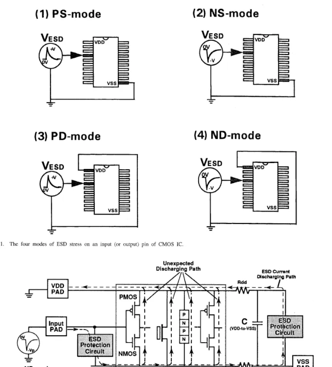
Besides, since ESD voltages may have positive or negative polarities to both Voo and V ~ S (ground), there are four ESD- stress conditions at each input (or output) pin as shown in Fig. 1.
PS Mode: ESD stress on a pin with positive voltage polarity to Vs,(GND) pin when
VDD
pin and other inputloutput pins are floating.NS Mode: ESD stress on a pin with negative voltage polarity to Vss(GND) pin when
VDD
pin and other inpudoutput pins are floating.PD Mode: ESD stress on a pin with positive voltage polarity to Voo pin when Vss(GND) pin and other input/output pins are floating.
ND Mode: ESD stress on a pin with negative voltage polarity to VDD pin when Vss(CND) pin and other inputloutput pins are floating.
These ESD voltages could damage both NMOS and PMOS devices in the input stage or output buffer of CMOS IC’s. In [9]-[l l], GCNMOS device is only arranged between the pad and Vss(GND). There is no ESD protection element arranged between the pad and VDD. In the ND-mode or PD-mode ESD stress, the internal circuits are dangerous to ESD damage. Fig. 2 shows a schematic diagram to explain the unexpected discharging paths in the internal part of a CMOS IC under the ND-mode ESD-stress condition, in which it only has an input-to-Vss ESD protection circuit at the input pad. The ND-mode ESD voltage between input pad and VDD pad is first transferred to the Vss power line through the input-to-Vss ESD protection circuit. This causes
308 IEEE TRANSACTIONS ON VERY LARGE SCALE INTEGRATION (VLSI) SYSTEMS, VOL. 4, NO. 3, SEPTEMBER 1996
( I )
PS-mode
(2!)
NS-mo
(3)
PD-mode
B
-
Fig. 1. The four modes of ESD stress on an input (or output) pin of CMOS IC
Unexpected
VDD-to-VSS ND-mode
ESD Voltage
Protection Fig. 2. Unexpected ESD discharging paths along the internal circuits beyond input-to-Vss ,and V o o -to-Vss ESD protection circuits.
voltage stress between VSS and VDD power lines. Due to the parasitic resistance and capacitance along VSS /VDD power lines in CMOS IC’s as well as the voltage drops on the input-to-Vss and VDD-to-Vss ESD protection elements, such nondirect ESD discharging path had been reported to cause some unexpected ESD damages on internal circuits beyond ESD protection circuits [12]-[16]. Thus, an ESD protection circuit for advanced submicron CMOS IC’s should perform
effective aind direct ESD discharging path from input and output pads to both VSS and VDD power lines. This is especially necessary for deep-submicron CMOS ASIC with larger chip size and longer vDD/vsS power lines which often surround the whole chip.
Moreover, in deep-submicron CMOS technology, the thick- ness of gate oxide had been scaled down to be thinner [2]. This much thinner gate oxide is more sensitive to ESD stress. For
KER et al.: CAPACITOR-COUPLE ESD PROTECTION CIRCUIT 309
Pad
VDD
7-
Thinner
7
Gate Oxide
Fig. 3.NMOS to clamp ESD voltage across the gate oxide of input stage.
A conventional input ESD protection circuit with gate-grounded
ESD protection of the input pad, the gate-grounded NMOS device is often used as the secondary protection element to clamp ESD voltage across the gate oxide of input stage.
A conventional input ESD protection circuit is shown in Fig. 3. ESD voltage across the input gate oxide is initially clamped by the snapback-trigger voltage (due to punchthrough or avalanche breakdown) of gate-grounded NMOS (171-[ 191. But, the voltage margin between gate-oxide breakdown and snapback breakdown is also much reduced in deep-submicron low-voltage CMOS technology. If the drain breakdown voltage of the gate-grounded NMOS is near to (or even higher than) the gate-oxide breakdown voltage, the gate oxide of input stage could be first ruptured by ESD voltage even if there is a gate- grounded NMOS to protect it. This condition is easy to happen, especially in deep-submicron low-voltage CMOS technology with much thinner gate oxide. Thus, the voltage difference between the gate-oxide breakdown and the drain snapback breakdown of short-channel NMOS device is an important voltage margin for ESD design.
In this paper, a capacitor-couple ESD protection scheme is proposed to overcome above issues. Not only to ensure uniform ESD current distribution but also to lower snapback- trigger voltage of NMOS and PMOS devices, this proposed capacitor-couple ESD protection circuit can perform effective ESD protection for deep-submicron low-voltage CMOS ASIC with thinner gate oxide. This work has been successfully verified in a 0.5 pm 3 V CMOS technology with thinner gate oxide of 90
A
[20].in MOS device [19]. The ESD robustness of MOS device is increased as its snapback voltage is decreased. Snapback voltage depends on device parameters such as junction profile, channel length, and gate bias. To find general application for on-chip ESD protection without modifying the CMOS process, the effort in this section is focused to find the dependence of gate bias on the snapback-trigger voltage of short-channel CMOS devices.
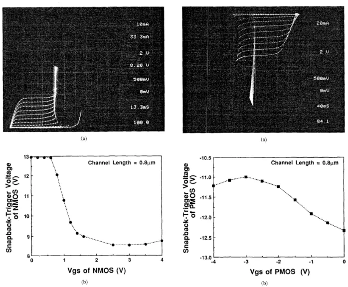
The curves shown in Fig, 4(a) are I-V characteristics of drain snapback breakdown
of
NMOS device with channel length of0.8
pm under various positive gate biases. As there is positive voltage on its gate, NMOS device is turned on to conduct current from drain to source. If drain voltage is still increased, NMOS will finally enter into its snapback region. In Fig. 4(a), the holding voltage for NMOS in its snapback region is about 8.2 V. Before thermal breakdown (or called as second breakdown), NMOS device can be safe in its snapback region to conduct current. But, the I-V curve for NMOS entering into its snapback region under positive gate bias is quite different to that of NMOS with gate grounded. The snapback-trigger voltage obviously decreases as its gate voltage increases. The dependence of this gate-biased effect on NMOS snapback-trigger voltage is shown in Fig. 4(b), where the snapback-trigger voltage can be lowered from 13 V to about 8.5 V. A short-channel PMOS also has similar I-V characteristics to those of NMOS due to lateral p-n-p bipolar action. Fig. 5(a) shows the I-V curvesof
PMOS device with channel length of 0.8 pm under various negative gate biases. The dependence of gate-biased effect on PMOS snapback- trigger voltage is shown in Fig. 5(b) where the magnitude of snapback-trigger voltage is reduced as its gate-to-source voltage V,, is more negative.This gate-biased effect on short-channel NMOS and PMOS devices lights us a way to more effectively protect the thin- ner gate oxide of deep-submicron low-voltage CMOS IC’s even without ESD-implant process. The holding voltage of snapback region in short-channel NMOS and PMOS de- vices due to lateral bipolar action is much lower than its drain snapback-breakdown voltage (under 0-V gate bias). If suitable ESD-transient voltage is coupled to the gate of ESD- protection NMOSPMOS device under ESD-stress condition, the snapback-trigger voltage of ESD-protection device can be reduced. Therefore, the lateral bipolar action in ESD- protection NMOSPMOS device can be earlier triggered on to bypass ESD current. Then, ESD voltage is clamped by the lower snapback holding voltage. Based on this concept, a capacitor-couple ESD protection circuit is proposed to ef- fectively protect the thinner gate oxide of CMOS devices in deep-submicron low-voltage CMOS ASIC without process modification to save fabrication cost.
11. CHARACTERISTICS OF CMOS 111. CAPACITOR-COUPLE ESD PROTECTION CIRCUIT
DEVICES FOR ESD PROTECTION
A. Circuit Configuration
The capacitor-couple ESD protection circuit for input pad to ensure uniform ESD current flow, as well as, to lower snapback-trigger voltage of ESD-protection devices is shown The operating region of gate-grounded NMOS device for
ESD protection is in its snapback region [18]. ESD failure threshold of MOS device was found to be strongly correlated to the snapback voltage of parasitic lateral bipolar action
310 IEEE TRANSACTIONS ON VERY LARGE SCALE INTEGRATION (VLSI) SYSTEMS, VOL. 4, NO. 3, SEPTEMBER 1996 L - 0
m
B9
-12.5 Ccn
2
o
-12.0 Channel Length = 0.8bm%
' 1 2 3 8 ' 0 Vgs of NMOS(V)
(b)Fig. 4. (a) The I-V characteristics of drain snapback breakdown of short-channel thin-oxide NMOS device with different gate biases from 0 to 5 V. (b) The dependence of gate-biased effect on NMOS snapback-trigger voltage.
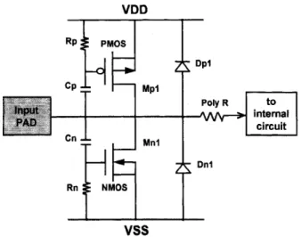
in Fig. 6. In Fig. 6, there is a thin-oxide PMOS (NMOS) de- vice Mpl (Mnl) arranged between input pad and VDD ( V S S ) . A capacitor C p ( C n ) is connected between the gate of Mpl (Mnl) and the input pad. A resistor
Rp(R,)
is connected between the gate of Mpl (Mnl) and VDD(VSS). The drainof Mpl (Mnl) is connected to the input pad, whereas the source of Mpl (Mnl) is connected to
Vo~(Vss).
There also exists a junction diode Dpl (Dnl) between the input pad and V D D ( V S S ) with its anode connected to the input pad (VSS) and its cathode connected to VOD (the input pad). This diode Dpl (Dnl) is inherently formed by the parasitic p - a junction between drain and bulk of Mpl (Mnl) device. A poly resistor R is connected from input pad to internal circuits.Capacitor C p ( C n ) is designed to couple suitable ESD- transient voltage to the gate of Mpl (Mnl) to lower snapback- trigger voltage of Mpl (Mnl). With lower snapback-trigger voltage, Mpl and Mnl can be earlier triggered into their snapback regions to bypass ESD current. Resistor
Rp(Rn)
is designed to sustain the coupled voltage longer in time on the-1a1.5 Channel Length = 0 . 8 ~ m
-...
m.
..
-...
-4 -3 -2 -1 0 vgs of PMOS (V) (b)Fig. 5 . (a) The I-V characteristics of drain snapback breakdown of
short-channel thin-oxide PMOS device with different gate biases from 0 to
-5 V. (b) ' f i e dependence of gate-biased effect on PMOS snapback-trigger voltage.
gate of Mpl (Mnl) to help Mpl (Mnl) device into its snapback region with lower snapback-trigger voltage. The four modes of ESD stress are one-by-one protected by this capacitor-couple ESD protection circuit to avoid the unexpected ESD damage in intem,al circuits.
B. Operating Principles
In normal CMOS operating condition with V ~ D and VSS power supplies, the high (low) voltage level of input signal is clamped by Dpl (Dnl) to about VO0
+
0.6 V (VSS - 0.6 V). Because the gate of Mpl (Mnl) is connected to V D D ( V S S ) through resistor Rp(R,), Mpl (Mnl) is always kept off during normal operations of CMOS IC's. Thus, the capacitor-couple ESD protection circuit is inactive as CMOS IC is in normal operating condition, as well as the voltage level of input signal can be clamped between V D D+
0.6 V andVSS
- 0.6 V.In ES:D-stress condition, there are four modes of ESD stress on a pad as those shown in Fig. 1. As PS-mode ESD stress
KER et al.: CAPACITOR-COUPLE ESD PROTECTION CIRCUIT 311 VDD
-
2-2-L
Poly R internal circuit Rnpq
p“’
vss
Fig. 6 . The proposed capacitor-couple ESD protection circuit.
occurs on the input pad of Fig. 6, ESD-transient voltage is coupled to the gate of Mnl through capacitor C,. Because ESD event is inherently a quick transition, capacitor C, can be designed to couple ESD-transient voltage to the gate of Mnl. This coupled voltage on the gate of Mnl leads to lower snapback-trigger voltage of Mnl to avoid overstress across the gate oxide of input stage. With lower snapback-trigger voltage, Mnl can be quickly triggered into its snapback region to bypass ESD current. ESD voltage on the pad is clamped to the snapback holding voltage of Mnl about 8.2 V, which is below the gate-oxide breakdown voltage. The suitable C, (R,) to couple (sustain) gate voltage for lowering snapback-trigger voltage of Mnl can be easily designed with consideration on device dimension of Mnl .
As NS-mode (PD-mode) ESD stress occurs on the input pad, diode Dnl (Dpl) is forward biased to bypass ESD current. The negative (positive) ESD voltage on the input pad will be clamped to about -0.6 V (+0.6 V), so the internal circuits can be protected against ESD damage. Diode under forward-biased condition can sustain very high ESD stress.
As ND-mode ESD stress occurs on the input pad with relatively grounded VDD, negative ESD-transient voltage is coupled to the gate of Mpl through capacitor C,. This coupled voltage on the gate of Mpl leads to lower snapback-trigger voltage to avoid overstress across the gate oxide of input stage. With lower snapback-trigger voltage, M pl can be quickly triggered into its snapback region to bypass ESD current and clamp the negative ESD voltage to its snapback holding voltage. Suitable C, (R,) to couple (sustain) gate voltage for lowering snapback-trigger voltage of M pl can be easily designed with consideration on device dimension of Mpl.
The four modes of ESD stress on the input pad are one-by- one protected by the capacitor-couple Mnl, diode Dnl, diode Dpl, and capacitor-couple Mpl, respectively. The magnitude and holding time of coupled voltage on the gate of Mnl (Mpl) can be adjusted by C, and R, (C, and R,) to make ESD-protection device active only in ESD-stress condition but inactive in normal operating condition of CMOS IC’s. A design model has been developed in next section to calculate
Metal PAD
Fig. 7. tion circuit.
Schematic cross-sectional view of the capacitor-couple ESD protec-
suitable C, and R, (C, and R p ) for this capacitor-couple ESD protection circuit.
C. Realization of Capacitor-Couple ESD Protection Circuit There are several ways to realize coupling capacitor and sustaining resistor in deep-submicron CMOS technology. The most efficient way to achieve this capacitor-couple effect without increasing total layout area to the pad has been shown in Fig. 7. In Fig. 7, it is a schematic cross-sectional view
of
this capacitor-couple ESD protection circuit, where then-
substrate twin-well CMOS technology is used to demonstrate device structure. This capacitor-couple ESD protection circuit can be realized in any CMOS or IBiCMOS technologies with p-well, n-well, or twin-well structure in p-type or
n-
type substrate. To achieve the capacitor-couple effect without increasing extra layout area to the pad, C, and C, are realized by inserting the poly layer right under the metal pad. R, and Rp are also realized by poly lines around the input pad. The capacitance of C, and C, can be adjusted by different overlap area between poly layer and metal pad. The resistance of
R,
and
R,
can be adjusted by different length of poly lines. A practical layout example in a 0.5 pm 3-V CMOS SRAM process is shown in Fig. 8 with device dimension of W / L = 500/1.0 (pm) for both Mnl and Mp l. In Fig. 8, Cn(Cp) is realized with capacitance of 0.2 pF. R,(Rp) is realized with resistance of 78 KO. Mnl and Mpl are surrounded by double guard rings( N +
and P+ diffusion) to prevent VDD-to-Vss latchup issue. The total layout area of this input cell (including the pad of 100 x 100 pm2 in Fig. 8 is only 307 x 144 pm2.I v . DESIGN MODEL OF CAPACITOR-COUPLE TECHNIQUE A design model is developed in ttis section to determine adequate coupling capacitance and sustaining resistance for the capacitor-couple ESD protection circuit, which is triggered on in ESD-stress condition but kept off in normal operating condition of CMOS IC’s.
A. Design Model of Capacitor-Couple ESD Protection Circuit An ESD-transient input waveform for model formulation is considered as a ramp voltage with peak voltage V, of 10 V and rise time t r of 10 ns as shown in Fig. 9. Since the gate- oxide thickness of CMOS devices in the 0.5-pm 3-V CMOS
312 IEEE TRANSACTIONS ON VERY LARGE SCALE INMGRATION (VLSI) SYSTEMS, VOL. 4, NO. 3, SEPTEMBER 1996
Fig. 8. A practical layout example of the capacitor-couple ESD protection circuit.
12
t F i O nsl
9
Vp4OV to simulate ESD transient10
r---
4----
- -.-
- I I I I I 0 10 20 30 40 50Time
(ns)
Fig. 9.breakdown for model derivation.
Input waveform to simulate ESD-transient voltage before gate-oxide
SRAM process is only 90
A,
such thinner gate oxide could beruptured if a voltage above 10 V is across it. So, the peak voltage V, in model derivation is set to 10 V. A normal input signal is also shown in Fig. 9 with peak voltage of 3 V and rise time of 10 ns to simulate normal input signal on the input pad. The capacitor-couple effect should be designed to trigger on the ESD-protection NMOSPMOS when the pad is under ESD stress. But, the ESD-protection NMOSPMOS should not be triggered on by any normal input signal when the pad is under normal operation of CMOS IC's. For simplicity, the capacitor-couple effect on ESD-protection NMOS and PMOS is separately considered in model derivation. The model formulation on half of capacitor-couple ESD protection circuit with Mnl device is described in the following.
The first step is to determine the operating region of NMOS in the capacitor-couple ESD protection circuit. To determine operating region of NMOS, the drain-source voltage V d s under various gate-source voltage
V,,
is classified. There are three operating regions of ESD-protection NMOS under PS-mode ESD stress.a) NMOS OFF, when
t
<
tr:
WhileVy,(t)
<
V,,,
NMOS is08:
b) NMOS ON, when t < t r :
As
Vg,(t)
2
V,,,
butVds(t)
> [Vgs(t)
-V,,],
NMOS is in saturation region;c) NMOS ON, when t
2
tr: NMOS remains in saturation region, because ofVds(t)
> [Vys(t)
-V,,].
The second step is to find the large-signal equivalent circuit of the capacitor-couple ESD protection circuit. The large- signal equivalent circuit of MOSFET with drain current and five parasitic capacitors is used in model derivation [21]. The resultant large-signal equivalent circuits of the capacitor- couple ES'D-protection NMOS under above three different operating regions are summarized in Fig. 10. With suitable linearization on parasitic capacitors of MOSFET [211 (which is estimateld as the average value over its operating region), each large-signal equivalent circuit of Fig. 10 can be treated as a linear circuit. The third step is to solve the coupled gate voltage in time domain. The solved V,,(t) corresponding to
KER et al.: CAPACITOR-COUPLE ESD PROTECTION CIRCUIT 313 Fig. 10. NMOS Vin Cdb
A---
Wn VP I I I 1iI Cdb wrl IUI
1
CdbThe large-signal equivalent circuits for the capacitor-couple ESD-protection NMOS device under three different operating regions. off (Vg3 < & h and t < tr). (b) Protection NMOS on (Vgs
2
Vth and t<
tr). (c) Protection NMOS on (Vgs2
T/th and t2
t r ) .as NMOS is in saturation region and t
<
tras NMOS is in saturation region but
t
2
tr
where R, is the sustaining resistance;V,, is the threshold voltage of NMOS;
(7%" is the total gate-drain capacitance of NMOS in ofs region, which includes C, ;
CfkT
is the total gate-drain capacitance of NMOS in saturation region, which includes C, ;( 2 ; :
" is the total gate-source capacitance of NMOS in ofs
region;
C;sT is the total gate-source capacitance of NMOS in saturation region;
Protection
V,,,
is the maximum voltage coupled to the gate of NMOS;V,
is the simulated peak voltage of ESD; tr is the rise time of ESD voltage; andt l is the time when the coupled gate voltage
Vg,(t)
first reaches the threshold voltage V,,.
The capacitance used in (1)-(3) is summarized in Table I. The coupled gate voltage
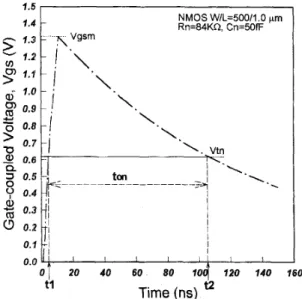
V,,(t)
in time domain calculated by above derived equations is shown in Fig. 11, which is triggered by a 10-V ramp voltage with rise time of 10 ns. The device dimension of ESD-protection NMOS in Fig. 11 is 500/1.0 (pm). The coupling capacitance C, is 50fF,
and the sustaining resistor R, is 84 KR. V,, is 0.635 V in the 0.5 pm 3 V CMOS S U M process. As seen in Fig. 11, the coupled gate voltage first rises up due to the 10 V ramp voltage applied to the input pad. This V,,(t) will reach its maximum314 IEEE TRANSACTIONS ON VERY LARGE SCALE INTEGRATION (VLSI) SYSTEMS, VOL. 4, NO. 3, SEPTEMBER 1996
TABLE I
NMOS USED IN THE DESIGN MODEL
CAPACITANCES OF CAPACITOR-COUPLE ESD-PROTECTION
C g
=Cn
+
Cox.
Wn.
L,
where Cox is the gate-oxide capacitance per unit area;
Cn
is
the coupling capacitance;Lo
is
the lateral diffusion;Ln
is
the channel lengthof NMOS;
Wn
is
the channel widthof
NMOS.
value
V,,,
on the time when the input ramp voltage reaches its peak value of 10 V. Larger C, will lead to higher V,,, on the gate of ESD-protection NMOS. Then, this coupled gate voltage is gradually discharged to 0 V through the resistor R,.Based on above model formulation, the maximum coupled gate voltage can be obtained by calculating (2) at
t
= tr, which is expressed asv,,,
=R,.
"Ptr
_ _
(4) The time
tl
when V,,(t) first rises up to reachV,,,
as well as the timet z
whenV,,(t)
falls belowV,,
again, are two important parameters in the design model. These two parameters are also indicated in Fig. 1 1. They can be obtained by setting (1) and (3) equal toV,,,
respectively. The timetl
and t 2 can be obtained as
and 1.58 1.4!
-
1.31 v)L
1.2>"
1.4 a,- 1.02
0.92
0.i' z 0 O.tt a, 0.G Q 3 0.!5 0y
0.4 a,2
0.3 c) 0.2 NMOS W/L=500/1.0 Fm Rn=84KQ. Cn=50fF.
20 40 60 80 l O q 120 140 160Time
(ns)
*
Fig. 11. The coupled voltage waveform of V,,(t) under the triggering of a
10 V ramp voltage with rise time of 10 ns, which is calculated by the derived design model.
The turn-on time of ESD-protection NMOS during ESD stress is an important factor to design suitable
C,
andR,
in the capacitor-couple ESD protection circuit. Usually, the NMOS tnrr-on time, ton, is designed in the range of 100-200 ns, which just fitted the transient duration of ESD stress. The turn-on time of ESD-protection NMOS can be obtained by
ton
= t z -t l .
(7)All above equations are derived from capacitor-couple ESD- protection NMOS in PS-mode ESD-stress condition. Similar design model for the half ESD-protection circuit from input pad to VDD with PMOS device in the ND-mode ESD-stress condition can be also obtained, if adequate replacement is made in the derived equations.
B. Comparison Between Model Calculation and HSPICE Simulation
The EISD protection circuit should be turned on only when the circuit is under ESD stress. The dependence of C, and
R,
(C, and R p ) on the coupled gate voltage of ESD- protection NMOS (PMOS) can be calculated by the derived design model. The accuracy of this design model is verified by HSPICE simulation.Fig. 12 and Fig. 13 show the dependence of NMOS turn- on time on the coupling capacitance C, and sustaining resistancie
R,
,
respectively, with both model-calculated and HSPICE-simulated results. The solid dots represent the HSPZCE-simulated results and the dashed lines show the model-calculated results. The NMOS turn-on time is nearly a linear function of C, in Fig. 12. Larger C, causes longer NMOS turn-on time to bypass ESD current. In Fig. 13, the NMOS iurn-on time is also nearly a linear function ofR,.
Larger
I?,,
also causes longer NMOS turn-on time to bypass ESD current. Fig. 14 shows the relation between the maximum coupled gate voltage (Vgsm) and C, under different R,. It isKER et al.: CAPACITOR-COUPLE ESD PROTECTION CIRCUIT 0 - 315 .-...*...*...*...*...e...',... Rn=IOKn
...
I I I I I I I I SPICE Simulation Model Calculation ... W/L=500/1 .O pm Vp=lOV, tr=lOns Vtn of NMOS = 0.635V....
350 300 n U) K-
250E
i=
2009
<
g
100c
E
150z
z
50 0 SPICE Simulation ... Model Calculation W/L=500/1 .O pm Vp=l OV, tr=l Oris Vtn of NMOS = 0.635V Cn=O.OGpF.
.
' \ . a ,** e' :' Cn=0.04pF..' ... .e :. .e . . 0 50 I00 150 200 250Sustaining Resistance, Rn (KR)
Fig. 13.sults about the effect Comparison between model-calculated and HSPICE-simulated re- of R, on NMOS turn-on time under different C , .
shown that larger C, and
R,
cause higher V,,, on the gate of ESD-protection NMOS.Fig. 15 depicts the overall effects between C, and
R,
under different NMOS turn-on time from 50 to 200 ns. For longer turn-on time, either R, or C, has to be designed with larger value. The undesired design region, shown in Fig. 15, means that the C, or R, are overdesigned in the capacitor-couple ESD protection circuit. This will cause voltage degradation on the normal 3 V input signal, because the voltage coupled to the gate of ESD-protection NMOS with such C, and R, is higher than its threshold voltage. So,R,
and C, in this undesired region should be avoided in this capacitor-1.6 1.4
-
1.22
6
0>
1.0 0.8 0.6 W/L=500/1 0 pm Vp=IOV, tr=lOns * e e * Rn=200KSZ, **a=
e** e e 0 Rn=lOKQ e 0 e.. SPICE Simulatior Model Calculatior 0.00 0.01 0.02 0.03 0.04 0.05 0.06 0.07 0.08 0.09Coupling Capacitance, Cn (pF)
Fig. 14. Comparison between model-calculated and HSPZCE-simulated re-
sults about the effect of C , on
v,,,
(maximum coupled gate voltage) under different R,.
320 300E
280 2602
240 220g
2003
180 v) 160 a, IY 140.-
p
120.-
.E loo v) 80 v) 60 (U 3 + 40 W/L=500/1 .O pm SPICE SimulationVp=l OV, tr=l Ons Model Calculation
Vtn of NMOS = 0.635V
...
e.i ton=200ns '\ \
\\ undesired design region
a.. \
.
-._
\ ".e \ ..Y \ - - ... e ....-.._
adequate design region \ \'-.-
...
20
0.00 0.01 0.02 0.03 0.04 0.05 0.06 0.07 0.08 0.09
Coupling Capacitance, Cn (pF)
Fig. 15.
time with both model-calculated and HSPZCE-simulated results.
Overall relation between C, and R, under different NMOS turn-on
couple ESD protection circuit. In the adequate design region of Fig. 15, the ESD-protection NMOS is not triggered on by the normal 3 V input signal, but it can be triggered on by the 10 V 10 ns ramp voltage under turn-on time from 50 to 200 ns. The adequate design region for R, and C, in Fig. 15 is located around the region of smaller value, so C, and R, can be practically realized by the poly layer as shown in Figs. 7 and 8 without occupying extra layout area.
Another issue on the capacitor-couple technique is the rise time of 10 V ramp voltage, which is used to simulate the ESD-transient voltage before the gate oxide of input stage is ruptured. In the design model, the rise time
tr
has beenIEEE TRANSACTIONS ON VERY LARGE SCALE INTEGRATION (VLSI) SYSTEMS, VOL. 4, NO. 3, SEPTEMBER 1996
W/L=500/1 .O prn SPICE Simulation Vtn of NMOS = 0.635V Model Calculation
turn-on time = 100ns
*
Vp=lOV5.
-.
I) 0.00 0.01 0.02 0.03 0.04 0.05 0.06 0.07 0.08 0.09Coupling Capacitance, Cn (pF)
Fig. 16. The relation of C , and R, to keep NMOS turn-on time of 100 ns
under different rise time of the 10 V ramp voltage.
SPICE Simulation Model Calculation ... W/L=500/1 .O prn Vtp of PMOS = -0.724V ... n ... U, c 300 . . - - a ' 6 ' " ' ... 6
.
I I I I I I I I 0.00 0.01 0.02 0.03 0.04 0.05 0.06 0.07 0.08 0.09Coupling Capacitance, Cp (pF)
Fig. 17.sults about the effect of C, on PMOS turn-on time under different R, .
Comparison between model-calculated and HSPICE-simulated re-
considered in equations (1)-(7). The sensitivity of t r on the design of R, and C, is analyzed in Fig. 16, where the NMOS turn-on time is kept as a constant of 100 ns. The peak voltage of ESD-simulated input voltage is still kept as 10 V, but its rise time is separately calculated with 1, 5, and 10 ns. In Fig. 16, it is shown that the variation between different curves due to different rise time of input ramp voltage is below 5%. Hence, the adequate design region in Fig. 15 for
R,
and C, is almost suitable for this capacitor-couple ESD protection circuit to protect both Human-Body-Model ESD stress (with rise time of 5-10 ns) and Machine-Model ESD stress (with rise time of 1-2 ns). SPICE Simulation ... Model Calculation. Vp=-1 OV, tr=lOns Vtp O f PMOS = -0.724V 350 n Y,, .
300F
250c
?
2w-
E
3 I- 150cn
02
100 - -a
0 50 100 150 200 250Sustaining Resistance, Rp
(KQ)
Fig. 18.sults about the effect of R, on PMOS tum-on time under different C,.
Companson between model-calculated and HSPICE-simulated re-
The dependence of PMOS turn-on time on coupling ca- pacitance C, and sustaining resistance R, is also calculated by the design model and compared with HSPZCE-simulated results in Figs. 17 and 18, respectively. The effect of C, and Rp on the PMOS turn-on time is similar to that of C, and R, on the NMOS turn-on time. The adequate design region and undesired design region about
R,
and C, for ESD-protection PMOS to accurately operate in CMOS IC's is shown in Fig. 19 with comparison to HSPZCE-simulated results. The adequate design region forRp
and C, in Fig. 19 is also located around the smaller-value region, so R, and C, for ESD-protection PMOS can be realized by the poly layer as shown in Figs. 7 and 8. This makes the capacitor-couple ESD protection circuit more suitable for high-pin-count CMOS IC's even in the pad-limite d condition.From Figs. 12 to 19, good agreement exists between HSPZCE-simulated and model-calculated results to verify this derived design model. With wide-range verification in the design model, suitable design of capacitor-couple ESD protection circuit can be easily obtained by this design model instead of iterative trial-and-error HSPICE simulation.
V. EXPERIMENTAL RESULTS
Based on the design model of capacitor-couple ESD pro- tection circuit, one set of test circuits with different device dimensions has been designed and fabricated in a 0.5 pm 3 V CMOS SlWM process. A microphotograph of the fabricated capacitor-couple ESD protection circuit is shown in Fig. 20, which is corresponding to the layout of Fig. 8. The test chip is assembled in IC package for ESD testing and for verification of capacit or-couple efficiency.
A. VeriJication of Capacitor-Couple Eficiency
To verify this capacitor-couple effect, an NMOS device with W / L = 20/1.0 (pm) is also on-chip designed with its gate
KER et al.: CAPACITOR-COUPLE ESD PROTECTION CIRCUIT 220 200
E
180 I? 160 140Q
.E 120 (II U) .Id2
100 mc
K a’a
v) 60 3.-
.-
.cI m m 20 W/L=500/1 .O pm 0 SPICE SimulationVp=-I OV, tr=lOns ... Model Calculation Vtp of PMOS -0.724V - . .- \
....
0 .. .-..__ ...e 0 adequate \ design region\\ .._ .... \ -\\\ undesired design region
ton=IOOns
7
- 0 . ....*...
\ \ CH 1A
t---L-J-
Input Pulse Generator (Hp81 16A) 300/1 .o 317 C H 2 Mn 2 2011 .oi
Rext=lKnl
v
T
1 1 I I-
-vss
Fig. 21. Experimental setup to measure the capacitor-couple efficiency in the capacitor-couple ESD-protection NMOS.
0.00 0.01 0.02 0.03 0.04 0.05 0.06 0.07 0.08 0.09
Coupling Capacitance, Cp (pF)
Fig. 19. Overall relation between C, and R, under different PMOS tum-on time with both model-calculated and HSPZCE-simulated results.
Fig. 22. Typical measured voltage waveforms in the setup of Fig. 21
(X-axis: 500 ns/div.; CH1: 5 V/div.; CH2: 0.5 V/div.). Fig. 20.
tion circuit.
A microphotograph of the fabricated capacitor-couple ESD protec-
connected to the gate of ESD-protection NMOS to monitor the coupled gate voltage. The setup to measure this capacitor- couple efficiency is shown in Fig. 21 with the monitor NMOS Mn2. A positive pulse-type voltage waveform with rise time of
5
ns (generated by pulse generator Hp8116A) is used to simulate ESD-transient voltage and applied to the input pad. This is to simulate the PS-mode ESD-stress condition. An oscilloscope is used to monitor the voltage waveform in time domain to investigate the capacitor-couple effect. The gate voltage of Mnl will arise from zero if a sharp-rising ESD-like voltage pulse is applied to the input pad. The voltage coupled to the gate of Mnl can be monitored by Mn2 device due to their gates are connected together. If the gate of Mnl (also of Mn2) is coupled to some voltage level through C,, Mn2 willbe tumed on to conduct current through the external resistor
Rext. Thus, the voltage at node ‘‘2” will be pulled down from
5
V synchronously when the input voltage pulse is applied.A typical measured result is shown in Fig. 22, where an input pulse with rising peak of 8.6 V (CH1) can cause a maximum voltage drop (at 2 node) of 1.77 V (CH2) from 5
V. This voltage drop on Rext of 1 KO causes a drain current
of 1.77 mA into Mn2. By measuring the I-V characteristics of a separated NMOS device which is the same as Mn2 in the same test chip, the corresponding maximum coupled voltage on the gate of Mnl can be found about 2.3 V. After capacitor coupling, the gate voltage of Mnl is discharged below V,, again by
R,.
Then, Mn2 is tumed off, and the voltage of node ‘‘2’’ will be restored to 5 V again as shown in CH2 ofFig. 22. In Fig. 22, the turn-on time of Mn2 (also of Mnl) is as long as 1.22 ps as the coupled gate voltage is still higher than
Vt,.
From above measured results, the coupling effect ofC,
and the voltage sustaining capability ofR,
can be verified. To verify the capacitor-couple efficiency amongC,,
R,,
and ESD-protection PMOS Mpl, a measurement setup is shown in Fig. 23 with an on-chip monitor PMOS Mp2 of W / L = 20/1.0 (pm). In Fig. 23, the gate voltage of Mpl drops from zero if a sharp-falling ESD-like negative voltage pulse is applied to the input pad. A pulse generator (HP81 16A) is used to apply a negative voltage pulse to the input pad (CH3) with VDD pad grounded. This is to simulate the ND- mode ESD-stress condition. The negative voltage coupled to the gate of Mpl through C, is monitored by Mp2. If the gate of Mpl (also of Mp2) is coupled to some negative voltage level, Mp2 will be turned on to conduct current to external
318
$
0.8IEEE TRANSACTIONS ON VERY LARGE SCALE IEJEGRATION (VLSI) SYSTEMS, VOL. 4, NO. 3, SEPTEMBER 1996
~ CH3
t
- CH4 1.00
E
*
T
Fig. 23.the capacitor-couple ESD-protection PMOS.
Experimental setup to measure the capacitor-couple efficiency in
Fig. 24.
axis: 500 ns/div.; CH3: 5 V/div.; CH4: 0.2 V/div.).
Typical measured voltage waveforms in the setup of Fig. 23 (X
resistor
Rext.
Thus, the voltage at node “Y” (CH4) in Fig. 23 is pulled up from -5 V synchronously when the input voltage pulse is applied.A typical measured result of capacitor-couple PMOS is shown in Fig. 24, where an input pulse with falling voltage peak of -8.2 V (CH3) and falling time of 5 ns can cause a maximum voltage increase of 0.32 V at node “Y” (CH4) from its initial bias of -5 V. This causes a drain current about 0.1 mA through Mp2 and Rext of 3 KO to the -5 V power supply. The corresponding maximum coupled voltage on the gate of Mpl can be found as 1.14 V. The negative gate voltage of Mpl will be discharged to become higher than
Vt,
again by Rp where V,, is the negative threshold voltage of PMOS. After the falling trigger, Mp2 is turned off and the voltage at node “Y” is restored to -5 V again. The turn-on time is about 1.66 ps.Fig. 25 shows the relation between the measured tum- on time of ESD-protection NMOSPMOS and the pulse- type trigger voltage on the input pad. The NMOS (PMOS)
a a
i
*
t at
I
A i 1 I I I’
0.5 4 6 8 10 12 0.6 2Trigger Voltage on Input Pad, IVtrig(
(w
Fig. 25. Measured results of turn-on time of capacitor-couple ESD-protection NMOS and PMOS with different input voltage peaks.
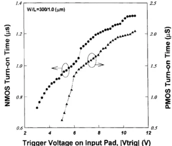
turn-on time increases as the magnitude of input voltage increases. The coupling capacitance and sustaining resistance in the test circuit are 0.14 pF and 140 KO, respectively, for both capacitor-couple NMOS and PMOS. In Fig. 25, the measured itum-on time of PMOS is longer than that of NMOS with the same trigger voltage on input pad. For symmetrical performance of ESD protection, the coupling capacitance and sustaining resistance have to be better designed with equal turn-on tirne in the ESD-protection NMOS and PMOS.
The experimental results shown here is just to demonstrate the fundamental function of coupling capacitance and sustain- ing resistance in the capacitor-couple ESD protection circuit. For practical applications in different submicron or deep- submicron CMOS technologies, C, (C,) and R,(R,) have to be adequately adjusted to meet the required turn-on time of ESD-protection device during ESD transition.
B. ESD Gsting Results
Two well-known industrial standards of ESD testing,
Human-J?ody-Model (HBM, MIL-STD-833C method
3015.7) and Machine-Model (MM, EIAJ-IC-121 method 20), are used to find the ESD failure threshold of the fabricated capacitor-couple ESD protection circuit in the four-mode ESD- stress conditions. The failure criterion is defined as the ESD voltage to cause input leakage current above 1 pA under 5-V
VDD
and 0-VVss
biases. ESD testing results (the ESD-pass voltage) of the fabricated test circuits with different device dimensions are listed in Table I1 (for HBM ESD testing) and Table I11 (for MM ESD testing), which are tested by the ESD tester HANWA HED-S5000 (produced in Japan). Without large device dimension but with lower trigger voltage to protect the thinner gate oxide, the capacitor-couple ESD protection circuit can pass the commercial specification of 2 KV HBM and 200 V MM ESD voltage. It is also found that the ESD-pass voltage is almost linearly increased as the channel width is increased either in HBM or MM ESD. In Table 11, theKER et al.: CAPACITOR-COUPLE ESD PROTECTION CIRCUIT
'
50011.2 50011.0 500lO.8 ND -240 -240 -220 PD 320 360 300 NS -550 -550 -550 319 500/0.6 4W1.0 3Ml1.2 -200 -200 -200 280 340 320 -550 -550 -550 ND PD-
P S 4 5 0 450 450 450 450 450 NS PS-
TABLE I1HUMAN-BODY-MODEL ESD TESTING RESULTS
( 5: Beyond 8KW
TABLE 111
MACHINE-MODEL ESD TESTING RESULTS
I I I 1 I I 3Mx1.8 3000.6
fi
' I ' I
4,75K1
5.5KI
(4 (b)Fig. 26. EMMI photograph of ESD-damaged hot spots among the multiple fingers of (a) capacitor-couple ESD-protection PMOS after ND-mode ESD stress and (b) capacitor-couple ESD-protection NMOS after PS-mode ESD stress.
shorter channel length of ESD-protection NMOS obviously performs a higher ESD-pass voltage under the PS-mode HBM ESD testing, because the shorter channel length leads to a higher current gain in the parasitic lateral bipolar action of ESD-protection NMOS device. This gives us a reference to choose suitable device dimension for practical applications.
C. Failure Analysis
The uniform current distribution in ESD protection devices was verified by using photon-emission microscopy (EMMI). Fig. 26 shows EMMI analysis of the capacitor-couple ESD
protection circuit after ESD stress. Fig. 26(a) presents the damaged hot spots on the capacitor-couple ESD-protection PMOS, which had been damaged by HBM ESD in the ND-mode condition. The damage on capacitor-couple ESD- protection NMOS due to PS-mode
HBM
ESD stress is shown in Fig. 26(b). The device dimensions ( W / L ) of ESD- protection NMOS and PMOS in Fig. 26 are both 500/1.0 (pm). In Fig. 26, all the five fingers of ESD-protection PMOS (NMOS) are uniformly turned on and damaged by the ND- mode (PS-mode) ESD voltage, This verifies the uniform turn-on characteristics of the capacitor-couple ESD protection circuit.320 IEEE TRANSACTIONS ON VERY LARGE SCALE INIXGRATION (VLSI) SYSTEMS, VOL. 4, NO. 3, SEPTEMBER 1996
VI. CONCLUSION
A capacitor-couple ESD protection circuit has been success- ful designed, fabricated, and verified in a
0.5-pm
3-V CMOS technology. Through capacitor-couple design, the PS-mode (ND-mode) ESD-transient voltage is coupled to the gate of ESD-protection NMOS (PMOS) to lower its snapback-trigger voltage, as well as to earlier trigger on the parasitic lateral bipolar action in the MOS device to bypass ESD current. The PD-mode (NS-mode) ESD voltage is clamped by the parasitic diode Dpl (Dnl) in the ESD-protection PMOS (NMOS). Thus, the thinner gate oxide in deep-submicron low-voltage CMOS technology can be effectively protected. With the poly layer inserting under the metal pad to realize the coupling capacitance and the poly lines extending around the pad to realize the sustaining resistance, a small layout area of the capacitor-couple ESD protection circuit has been demonstrated without increasing extra layout area to the IC chip. A timing- original design model has been also derived to calculate the capacitor-couple efficiency for the capacitor-couple ESD protection circuit without trial-and-error HSPICE simulation. Experimental results have verified that this capacitor-coupl‘e technique can offer more effective ESD protection for the thinner gate oxide. Not only to ensure uniform ESD current distribution among the multiple fingers of ESD-protection devices but also to earlier trigger on the ESD-protection devices to bypass ESD current, the ESD-pass voltage is found to be higher than 2 KV and 200 V in HBM and MM ESD testing, respectively. The ESD-pass voltage is linearly increased as the device dimension of ESD-protection NMOSPMOS is increased. The proposed capacitor-couple ESD protection circuit is very suitable for deep-submicron low-voltage CMOS ASIC in the high-pin-count or the pad- limited application to save silicon cost. This capacitor-couple technique can be also applied to the CMOS output buffer to improve ESD robustness of the output pad.ACKNOWLEDGMENT
The authors wish to thank Mr. C.-N. Wu and Mr. T.-L. Yu for their help in chip fabrication and ESD testing. This work was also awarded the 1995 Long-Terng Thesis Award from Acer International, Inc., Taiwan.
REFERENCES
[I] C. Duvvury and A. Amerasekera, “ESD: A pervasive reliability concem for IC technologies,” Proc. IEEE, vol. 81, pp. 690-702, May 1993. [2] A. Amerasekera and C. Duvvury, “The impact of technology scaling
on ESD robustness and protection circuit design,” in EOS/ESD Symp.
Proc., vol. EOS-16, 1994, pp. 237-245.
[3] S. Daniel and G. Krieger, “Process and design optimization for advanced CMOS U 0 ESD protection devices,” in EOS/ESD S-ymp. Proc., vol. EOS-12, 1990, pp. 206-213.
[4] C. Diaz, T. Kopley, and P. Marcoux, “Building-in ESDEOS reliability for sub-halfmicron CMOS processes,” in Proc. IRPS, pp. 276283, 1995.
[5] ,A. Chatterjee and T. Polgreen, “A low-voltage triggering SCR for on- chip ESD protection at output and input pads,” IEEE Electron Device
Lett., vol: 12, pp. 21-22, Jan. 1991.
[6] M.-D. Ker et al., “Complementary-LVTSCR ESD protection scheme for submicron CMOS IC’s,” in Proc. IEEE Int. Symp. Circuits Syst., 1995, pp. 833-836.
M.-D. Pkr et al., “Area-efficient CMOS output buffer with enhanced high ESD reliability for deep submicron CMOS ASIC,” in Proc. 8rh
IEEE Int. ASIC Con$ Exhibit, 1995, pp. 123-126.
M.-D. K i r and C.-Y. Wu, “Modeling the positive-feedback regenerative process of CMOS latchup by a positive transient pole method: Part I-Theoretical derivation,” IEEE Trans. Electron Devices, vol. 42, pp.
1141-1148, June 1995.
C. Duvvury and C. Diaz, “Dynamic gate coupling of NMOS for efficient output ESD protection,” in Proc. IRPS, 1992, pp. 141-150.
C. Duvvury, C. Diaz, and T. Haddock, “Achieving uniform nMOS device power distribution for submicron ESD reliability,” in Tech. Dig.
IEDM, 1992, pp. 131-134.
S. Ramaswamy, C. Duvvury, and S.-M. Kang, “EOSESD reliability of deep sub-micron NMOS protection devices,” in Proc. IRPS, 1995, pp. 284-291,
C. Duvvury, R. N. Rountree, and 0. Adams, “Internal chip ESD phe- nomena beyond the protection circuit,” IEEE Trans. Electron Devices,
vol. 35, pp. 2133-2139, Dec. 1988.
C. Coosk and S. Daniel, “Characterization of new failure mechanisms arising from power-pin ESD stressing,’’ in EOSIESD Symp. Proc., 1993, M. D. Jaffe and P. E. Cottrell, “Electrostatic discharge protection in a 4-Mbit DRAM,” in EOS/ESD Symp. Proc., 1990, vol. EOS-12, pp. 2 18-223.
C. C. Johnson, T. J. Maloney, and S. Qawami, “Two unusual HBM ESD failure mechanisms on a mature CMOS process,” EOS/ESD Symp.
Proc., 1993, vol. EOS-15, pp. 225-231.
H. Terletzki, W. Nikutta, and W. Reczek, “Influence of the series resistance of on-chip power supply buses on intemal device failure after ESD stress,” IEEE Trans. on Electron Devices, vol. 40, no. 11, pp. 2081-2083, 1993.
F.-C. Nsu, P.-K. KO, S. Tam, C. Hu, and R. S . Muller, “An analytical breakdlown model for short-channel MOSFET’s,” IEEE Trans. Electron
Devices, vol. 29, pp. 1735-1740, Nov. 1982.
Y. Fong and C. Hu, “High-current snapback characteristics of MOS- FET’s,” lEEE Trans. Electron Devices, vol. 37, pp. 2101-2103, 1990. K.-L. Chen, “The effects of interconnect process and snapback voltage on the ESD failure threshold of NMOS transistor,” IEEE Trans. Electron
Devices, vol. 35, pp. 2140-2150, Dec. 1988.
M.-D. Ker et al., “On-chip ESD protection using capacitor-couple technique in 0.5-pm 3-V CMOS technology,” in Proc. 8th IEEE Int.
ASIC Con$ Exhibit, 1995, pp. 135-138.
C.-Y. Wu, J . 4 . Hwang, C. Chang, and C.-C. Chang, “An efficient timing modell for CMOS combination logic gates,” IEEE Trans. Computer-
Aided Devices Integr. Circuits Syst., vol. CAD-4, pp. 636-650, 1985.
vol. EOS-15. pp. 149-156.
Ming-Dou Ker (S’92-M’94) was born in Taiwan,
ROC, in 1963. He received the B.S. degree from the Department of Electronics Engineering, and the M.S. and Ph.D. degrees from the Institute of Elec- tronics, National Chiao-Tung University, Hsinchu, Taiwan, in 1986, 1988, and 1993, respectively.
From 1993 to 1994, he was a postdoctoral re- searcher in Integrated Circuits and Systems Lab- oratory, Institute of Electronics, National Chiao- Tung University, Hsinchu, Taiwan. In 1994, he ioined the VLSI Design Denartment of Comouter “ I
and Communication Research Laboratories (CCL), Industrial Technology Research Institute (ITRI), Hsinchu, Taiwan, as a circuit design engineer. Since then, he has been engaged in the development of mixed-mode integrated circuits in submicron CMOS technology. His research interests include reliability of CMOS integrated circuits, mixed-mode integrated circuits, and communication integrated circuits design.
KER et al.: CAPACITOR-COUPLE ESD PROTECTION CIRCUIT 321
Chuug-Yu Wu (S’75-M’77) was horn in Chiayi, Taiwan, ROC, in 1950. He received the M.S. and Ph.D. degrees from the Department of Electronics Engineering, National Chiao-Tung University, Tai- wan, in 1976 and 1980, respectively.
From 1980 to 1984, he was an Associate Profes- sor in the National Chiao-Tung University. During 1984-1986, he was a Visiting Associate Professor in the Department of Electrical Engineering, Portland State University, OR. Since 1987, he has heen a
Professor in the National Chiao-Tung University.
Tao Cheng was bom in Kaoshung, Taiwan, ROC, in 1971. He received the B.S. degree in 1993
from the Department of Electronics Engineering, and the M.S. degree in 1995 from the Institute of Electronics, National Chiao-Tung University, Tai- wan.
He had been engaged in development of CMOS on-chip ESD protection circuits and the failure anal- ysis of ESD damages, with the support from Win- bond Electronics Corporation, Science-Based Park, Hsinchu, Taiwan. His master thesis was awarded the From 1991 to 1995, he was rotated to serve as Director of the Division of
Engineering and Applied Science in the National Science Council. Currently, he is the Centennial Honorary Chair Professor at the National Chiao-Tung University. He has published more than 60 joumal papers and 90 conference papers on several topics, including digital integrated circuits, analog integrated circuits, computer-aided design, neural networks, ESD protection circuits, special semiconductor devices, and process technologies He also has 10 patents including five U.S. patents. His current research interests focus on low-voltage low-power mixed-mode integrated circuit design, hardware implementation of visual and auditory neural systems, and RF integrated
circuit design. University.
Dr Wu is a member of Eta Kappa Nu and Phi Tau Phi. He was awarded the Outstanding Research Award by the National Science Council in 1989 and 1995, and the Outstanding Engineenng Professor by the Chinese Engineer
Association in 1996. munications.
1995 Long-Temg Thesis Award from Acer Intemational Inc., Taiwan. He is now serving in the Army of the Republic of China.
Hun-Hsien Chang (S’93) was hom in Taipei, T a - wan, ROC, in 1964 He received the B.S. degree
from the Department of Electronics Engineering, National Chiao-Tung University, Hsinchu, Taiwan, in 1991. He is workmg toward the P h D degree in the Institute of Electronics, National Chiao-Tung Presently, his current research interests include I/O interface circuit, ESD protection circuit, and CMOS mixed-mode IC’s for high-speed data com-