電信工程學系
碩 士 論 文
並聯 RC 回授與變壓器雜訊抵消之
超寬頻低雜訊放大器設計
Parallel-RC Feedback and Transformer Noise-
Canceling Low Noise Amplifiers for
UWB Application
研 究 生:何廣琪
指導教授:唐震寰 教授
Parallel-RC Feedback and Transformer Noise-Canceling
Low Noise Amplifiers for UWB Application
研 究 生:何廣琪 Student:Kuang-Chi He
指導教授:唐震寰 教授 Advisor:Dr. Jenn-Hwan Tarng
國 立 交 通 大 學
電 信 工 程 學 系
碩 士 論 文
A Thesis
Submitted to Department of Communication Engineering College of Electrical Engineering and Computer Science
National Chiao Tung University in Partial Fulfillment of the Requirements
for the Degree of Master
in
Communication Engineering
July 2009
Hsinchu, Taiwan, Republic of China
I
超寬頻低雜訊放大器設計
研究生:何廣琪 指導教授:唐震寰
國立交通大學
電信工程學系 碩士班
摘要
本論文提出了一個利用並聯RC回授與一個利用變壓器達成雜訊抵消的超寬 頻低雜訊放大器設計。我們所提出的電路使用TSMC 0.18-μm CMOS 製程技術製 作完成。 第一個電路我們使用RC並聯回授和一個源極電感來達成寬頻阻抗匹配並有 效的降低雜訊。再利用並聯LC網路更進一步的壓制高頻雜訊達成很低的雜訊水平。 量測結果為最低的雜訊指數為2.5 dB。在3.1-10.6 GHz的功率增益為10.9-13.9 dB。在3.1-15 GHz的輸入返回損耗為-9.4至-32.4 dB。在1.4V偏壓下的消耗功率 為14.4 mW,整體面積為0.46 mm2 。 第二個電路我們使用一個變壓器輸入級達成寬頻的雜訊抵消與輸入阻抗匹 配,並只需要小的晶片面積與低的消耗功率。量測結果為最低的雜訊指數為3.8 dB。在3.1-10.6 GHz內的功率增益大於10.2 dB。在3.1-13 GHz內的輸入返回損 耗低於-10.1 dB。在1.2V偏壓下的消耗功率為9.7 mW,整體面積為0.47 mm2 。II
Canceling Low Noise Amplifiers for
UWB Application
Student:Kuang-Chi He Advisor:Dr. Jenn-Hwan Tarng
Department of Communication Engineering
National Chiao Tung University
Abstract
In this thesis, a parallel-RC feedback and a transformer noise-canceling low noise amplifier for ultra-wide-band applications are presented. These propose circuits are implemented by the TSMC 0.18-
μ
m CMOS process.In our first design, the parallel-RC shunt feedback with a source inductance is proposed to obtain the broadband input matching and to reduce noise level effectively. The parallel-LC network at drain is drawn to further suppress the high-frequency noise and a low noise level is achieved. Measured results show that minimum noise figure is 2.5 dB. The power gain is 10.9-13.9 dB from 3.1 to 10.6 GHz. The input return loss is below -9.4 dB from 3.1 to 15 GHz. It consumes 14.4 mW from 1.4 V supply voltage and occupies an area of only 0.46 mm2.
In our second design, a transformer input stage is proposed to achieve broadband noise cancellation and input matching with small chip area and low power consumption. Measured results show that minimum noise figure is 3.8 dB. The power
III
10.1 dB from 3.1 to 13 GHz. It consumes 9.7 mW from 1.2 V supply voltage and occupies an area of only 0.47 mm2.
IV
誌
謝
在新竹交通大學碩士班的這二年歲月裡,誠心的感謝我的指導教授 唐震寰 老師提供我一流的實驗室學習環境與專業上的指導。讓我對於射頻電路能夠有著 非常多的進步與了解。雖然新竹的食物有些並不怎美味,但是交通大學還是一個 非常好的地方,在學習鑽研知識上是一個很讓人讚賞的地方。 在這滿滿回憶的兩年生活裡,感謝梁小姐每天幫我們處理那麼多事情,真的 很辛苦。感謝 810 實驗室的博班學長標哥與佩宗平時幫我們解決那麼多問題與教 導我們。感謝學長雅仲、焯基哥與俊彥哥一起度過了愉快的一年。感謝學弟冠豪、 國政、鉦浤與耿賢的陪伴。感謝共同在一起兩年同樂同患難的夥伴明宗、政銘與 兆凱。 在這兩年的求學生涯裡,感謝我的家人一直陪伴著我與鼓勵著我,讓我有著 一個避風港,很累時可以回家休息充電。在交大讀書的這兩年裡,充滿著許多的 回憶,遇見了很多人,祝大家都能很快樂幸福,完成自己的夢想。 何廣琪 誌予 九十八年七月V
CONTENTS
ABSTRACT (CHINESE) ... Ⅰ
ABSTRACT (ENGLISH) ... Ⅱ
ACKNOWLEDGEMENT ... Ⅳ
CONTENTS ... Ⅴ
LIST OF TABLES ... Ⅷ
LIST OF FIGURES
...Ⅸ
CHAPTER 1
Introduction
1
1.1 Related Works and Motivation ... 1
1.2 Thesis Organization ... 2
CHAPTER 2
Basics of LNA Design
3
2.1 Effects of Nonlinearity ... 3 2.1.1 Harmonics ... 3 2.1.2 Gain Compression ... 4 2.1.3 Inter-modulation ... 4 2.2 Noise ... 7 2.2.1 Thermal Noise ... 7 2.2.2 Flicker Noise ... 9VI
2.2.4 Noise Figure ... 10
2.2.5 Noise Figure of Cascaded Stages ... 11
2.3 Sensitivity and Dynamic Range ... 13
2.3.1 Sensitivity ... 13
2.3.2 Spurious-Free Dynamic range (SFDR) ... 14
2.4Topologies Low Noise Amplifiers ... 16
2.4.1 Input Matching ... 16
2.4.2 Summary ... 21
2.5 Bandwidth Techniques ... 23
2.5.1 Shunt Peaking ... 23
2.5.2 Triple-Resonance Architecture ... 25
CHAPTER 3
Design of Parallel-RC feedback UWB LNA
27
3.1Circuit Design and Analysis ... 283.1.1 Input Stage ... 28 3.1.2 Second Stage ... 32 3.1.3 Output Buffer ... 34 3.1.4 Noise Analysis ... 34 3.2 Experimental Results ... 35 3.3 Summary ... 39
VII
4.1 Noise-Canceling Principle ... 40
4.2 Circuit Design of The Noise-Canceling UWB LNA ... 43
4.2.1 Input Match ... 44 4.2.2 Noise Analysis ... 45 4.3 Experimental Results ... 48 4.4 Summary ... 52
CHAPTER 5
Conclusion
53
REFERENCES ... 55
VIII
Table Ⅰ Six input matching architectures summary ... 22 Table Ⅱ Measured Performance Summary and Comparison ... 39 Table Ⅲ Measured Performance Summary and Comparison ... 51
IX
Figure 2.1 Definition of the 1-dB compression point ... 4
Figure 2.2 Corruption of a signal due to inter-modulation between two interferers ... 5
Figure 2.3 The third-order intercept point in a two-tone inter-modulation test ... 6
Figure 2.4 (a) Graphical interpretation of IIP3, (b) calculation of IIP3 without extrapolation ... 7
Figure 2.5 Thermal noise of a resistor: (a) equivalent series voltage source, (b) equivalent parallel current source ... 8
Figure 2.6 Thermal noise of a MOSFET ... 8
Figure 2.7 Dangling bonds at the oxide-silicon interface ... 9
Figure 2.8 Representation of noise by input noise generators ... 10
Figure 2.9 Cascaded noisy stages ... 11
Figure 2.10 Spurious-free dynamic range ... 15
Figure 2.11 Common-source amplifier with shunt input resistor ... 16
Figure 2.12 Resistive shunt feedback ... 17
Figure 2.13 Common-gate stage ... 18
Figure 2.14 Resistive termination by Inductive degeneration ... 19
Figure 2.15 Multistage input filter ... 20
Figure 2.16 Basic distributed amplifier ... 21 Figure 2.17 Shunt peaking a common source amplifier. (a) Simple common source
amplifier and (b) its equivalent small signal model. (c) Common source amplifier with shunt peaking and (d) its equivalent small signal model
X
Figure 2.18 Frequency response of shunt-peaking amplifier for three cases ... 24
Figure 2.19 (a) Inductively peaked stage, (b) TRA ... 26
Figure 2.20 Behavior of a triple-resonance circuit at different frequencies ... 26
Figure 2.21 frequency response of the TRA ... 26
Figure 3.1 Proposed UWB LNA ... 27
Figure 3.2 (a) Miller equivalent circuit. (b) series converted to parallel of equivalent circuit ... 28
Figure 3.3 Effect of CF on input impedance ... 30
Figure 3.4 Effect of RF on NF ... 30
Figure 3.5 Equivalent circuit for suppressing thermal noise of RL1 ... 31
Figure 3.6 Effect of LD, CD, and LS1 on NF of input stage ... 32
Figure 3.7 I-V characteristics of MOSFET with and without FBB ... 32
Figure 3.8 Simulation frequency response of input stage, second stage, and overall stage ... 34
Figure 3.9 Noise equivalent circuit of input stage ... 35
Figure 3.10 Chip microphotograph of the UWB LNA ... 36
Figure 3.11 Measured and simulated power gain (S21) and input return loss (S11) of the UWB LNA ... 37
Figure 3.12 Measured and simulated output return loss (S22) and reverse isolation (S12) of the UWB LNA ... 37
Figure 3.13 Measured and simulated noise figure of the UWB LNA ... 38
Figure 3.14 Measured IIP3 at 8 GHz ... 38
Figure 4.1 Principle of the noise-canceling technique ... 40
Figure 4.2 Proposed noise-canceling technique ... 42
XI
Figure 4.5 Computed NF of LNA with M3 turned ON and OFF ... 47
Figure 4.6 Simulated S parameters of LNA with M3 turned ON and OFF ... 47
Figure 4.7 Chip microphotograph of the noise-canceling LNA ... 49 Figure 4.8 Measured and simulated power gain (S21) and input return loss (S11)
of the noise-canceling LNA ... 49 Figure 4.9 Measured and simulated output return loss (S22) and reverse isolation
(S12) of the noise-canceling LNA ... 50 Figure 4.10 Measured and simulated noise figure of the noise-canceling LNA .. 50 Figure 4.11 Measured IIP3 at 6 GHz ... 51
1
Chapter 1 Introduction
1.1 Related Works and Motivation
In recent years, Ultra-wide-band (UWB) systems have attracted more interest due to their capability of transmitting data with high data rate and low power consumption. For IEEE 802.15.3a standard, the allocated band of UWB is between 3.1-10.6 GHz. The wide-band low noise amplifier (LNA) for wireless front-end radio frequency receiver is a critical block. Since the LNA is the first gain stage in the receive path, its noise figure directly adds to that of the system. Thus the LNA needs to fulfill several requirements, such as broadband input matching, sufficient power gain, and low noise figure, etc.
Recently, CMOS technology has suddenly become the topic of active research because of its low cost, low power, and high integration. Several major types of UWB CMOS LNAs have been reported. However, LNA’s performances almost always involve trade-offs. For example, although the distributed amplifier (DA) provides good wideband input matching and flat gain, it consumes more power and chip area. The resistive shunt feedback is a well-known wide band technique, which provides wide band input matching but increases NF due to the local feedback [1]. The inductive degeneration can only provide a narrowband input matching but it can achieve better noise performance [2]. Another technology is to use a multistage input filter for broadband input matching [3]. However, the input filter insertion loss degrades the LNA’s NF, and a large chip area is unavoidable.
2
To solve these problems, a parallel-RC feedback and a transformer noise-canceling LNAs are presented for UWB applications. In our first design, the parallel-RC shunt feedback with a source inductance is proposed to obtain the broadband input matching and to reduce noise by the local feedback effectively. The parallel-LC network at drain is drawn to further suppress the high-frequency noise and a low noise level is achieved. It needs only a small inductor for broadband matching, so chip area can be realized in a small area. In our second design, a transformer input stage is proposed to achieve broadband noise cancellation and input matching. The proposed noise-canceling technique can achieve noise cancellation and signal addition without high-Q inductors, so it can be realized in a small chip area with low power consumption.
1.2 Thesis Organization
The thesis consists of five chapters. Chapter 1 gives a introduction. Chapter 2 describes basic concepts in LNA design, emphasizing the effects of noise and nonlinearity. Chapter 3 discusses a parallel-RC feedback UWB LNA with simulation and measured results. In the Chapter 4, a broadband noise-canceling LNA using transformer is introduced. Eventually, all the work is summarized and concluded in Chapter 5.
3
Chapter 2 Basics of LNA Design
2.1 Effects of Nonlinearity
While many RF circuits can be approximated with a linear model to obtain their response to small signals, nonlinearities often lead to interesting and important phenomena. For a nonlinear system, the input-output relationship can be approximated as
2
3
1 2 3
y t x t x t x t (2.1)
Equation (2.1) can help us to understand some effects of nonlinearity.
2.1.1
Harmonics
If a sinusoid is applied to a nonlinear system, the output generally exhibits frequency components that are integer multiples of the input frequency. In (2.1), if x(t)=Acosωt, then
2 2 3 31 cos 2 cos 3 cos
y t A t A t A t (2.2)
2 2 3 3
1 cos 1 cos 2 3cos cos3
2 4 A A A t t t t (2.3) 3 3 2 2 3 3 2 2 1 3
cos cos 2 cos3
2 4 2 4
A A
A A
A t t t (2.4)
In Eq. (2.4), the term with the input frequency is called the “fundamental” and higher-order terms the “harmonics”.
4
2.1.2
Gain Compression
The small-signal gain of a circuit is usually obtained with the assumption that harmonics are negligible. In fact, nonlinearity can be viewed as variation of the small-signal gain with the input level. As the signal amplitude increases, the gain begins to vary. In most circuits of interest, the output is a “compressive” or “saturating” function of the input; that is, the gain approaches zero for sufficiently high input levels. In (2.14) this occurs if α3 < 0. Written as
α1+3α3A2/4, the gain is therefore a decreasing function of A. In RF circuits, this effect is
quantified by the “1-dB compression point”, defined as the input signal level that caused the small-signal gain to drop by 1 dB (Fig. 2.1).
1 dB
1 dB
A 20logAin
20logAout
Figure 2.1 Definition of the 1-dB compression point.
2.1.3
Inter-modulation
When two signals with different frequencies are applied to a nonlinear system, the output in general exhibits some components that are not harmonics of the input frequencies. Called inter-modulation (IM), this phenomenon arises from “mixing” (multiplication) of the two signals when their sum is raised to a power greater than unity. We assume x(t)=A1cosω1t+A2cosω2t. Thus,
5
2 1 1cos 1 2cos 2 2 1cos 1 2cos 2y t A t A t A t A t
3
3 A1cos 1t A2cos 2t (2.5)
Expanding the left side and discarding DC terms and harmonics, we obtain the following inter-modulation products:
1 2: 2A A1 2cos 1 2 t2A A1 2cos 1 2 t (2.6)
3 12 2 3 12 2 1 2 1 2 1 2 3 3 2 : cos 2 cos 2 4 4 A A A A t t (2.7)
3 22 1 3 22 1 2 1 2 1 2 1 3 3 2 : cos 2 cos 2 4 4 A A A A t t (2.8)and these fundamental components
3 2 3 2 1 2 1 1 3 1 3 1 2 1 1 2 3 2 3 2 1 2 3 3 3 3 , : cos cos 4 2 4 2 A A A A t A A A A t (2.9)
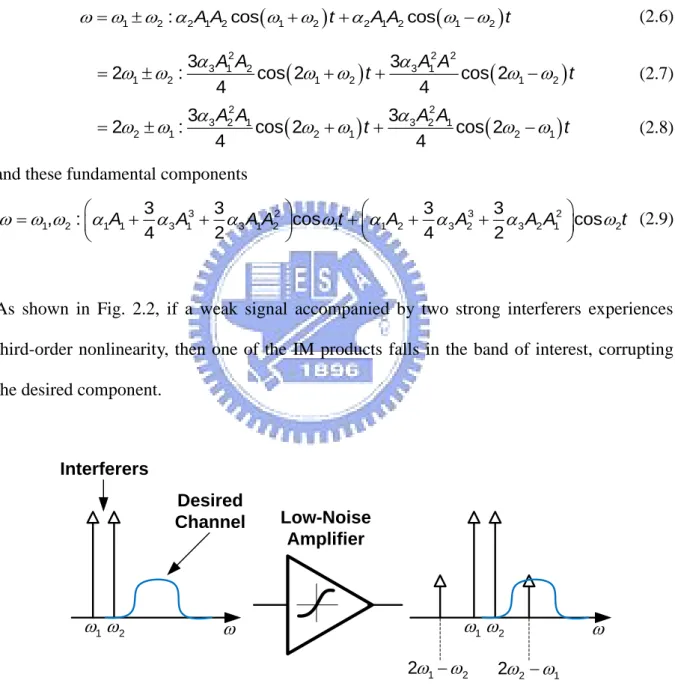
As shown in Fig. 2.2, if a weak signal accompanied by two strong interferers experiences third-order nonlinearity, then one of the IM products falls in the band of interest, corrupting the desired component.
Interferers Desired Channel Low-Noise Amplifier 12 1 2 2 221 12
6
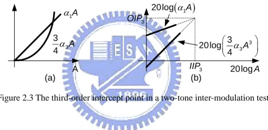
This phenomenon can be measured by a two-tone test in which A is chosen to be sufficiently small so that higher-order nonlinear terms are negligible and the gain is relatively constant and equal to α1. From (2.7), (2.8), and (2.9), we note that as A increases, the fundamentals
increase in proportion to A, whereas the third-order IM products increase in proportion to A3. Plotted on a logarithmic scale, the magnitude of the IM products grows at three times the rate at which the main components increase. As shown in Fig. 2.3, the third-order intercept point is defined to be at the intersection of the two lines. The horizontal coordinate of this point is called the input IP3 (IIP3), and the vertical coordinate is called the output IP3 (OIP3).
A (a) (b) 1A 3 3 4 A
1
20log A 3 3 3 20log 4 A 3 OIP 3 IIP 20log AFigure 2.3 The third-order intercept point in a two-tone inter-modulation test.
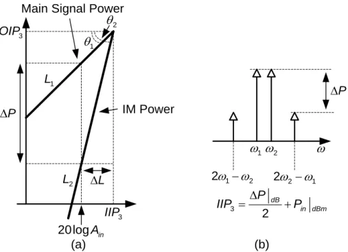
In Fig. 2.4(a), ΔL×tanθ2-ΔL×tanθ1=ΔP, tanθ2=3tanθ1, and tanθ1=1, we can obtain ΔL=
ΔP/2, and
3 1, 2 3
1
20 log 20 log 20 log 20 log
2
IP IM in
A A A A (2.10)
That is, if all the signal levels are expressed in dBm, the IIP3 is equal to half the difference between the magnitudes of the fundamentals and the IM3 products at output plus the corresponding input level.
7
IM Power Main Signal Power
(b) (a) 12 1 2 2 221 P 3 2 dB in dBm P IIP P 20logAin 3 IIP 3 OIP P L 1 L 2 L 1 2
Figure 2.4 (a) Graphical interpretation of IIP3, (b) calculation of IIP3 without extrapolation.
2.2 Noise
Noise can be loosely defined as any random interference unrelated to the signal of interest. In this subsection, we will introduce two major noise sources in RF circuit, some definition, and noise analysis technique.
2.2.1
Thermal Noise
Present in all circuits is thermal noise, generated by resistors, base and emitter resistance of bipolar devices, and channel resistance of MOSFETs.
Resistor Thermal Noise The random motion of electrons in a conductor introduces
fluctuations in the voltage measured across the conductor even if the average current is zero. Thus, the spectrum of thermal noise is proportional to the absolute temperature.
8 Noiseless Resistor - + Noiseless Resistor (a) (b) 2 n V R R 2 n I
Figure 2.5 Thermal noise of a resistor: (a) equivalent series voltage source, (b) equivalent parallel current source.
As shown in Fig. 2.5, the thermal noise of a resistor R can be modeled by a series voltage source or a parallel current source.
2 4 n V kTR f (2.11) 2 4 n I kT R f (2.12)
Where k=1.38×10⁻²³J/K is the Boltzmann constant.
MOSFETs MOS transistors also exhibit thermal noise. The most significant source is the
noise generated in the channel. The channel noise can be modeled by a current source connected between the drain and source terminals.
2
0
4
n d
I kT g (2.13)
Where gd0 is the drain-source conductance with VDS=0.
2
n
I
9
2.2.2
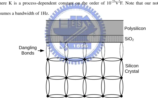
Flicker Noise
The interface between the gate oxide and the silicon substrate in a MOSFET entails an interesting phenomenon. Since the silicon crystal reaches an end at this interface, many “dangling” bonds appear, giving rise to extra energy states (Fig. 2.7). As charge carriers move at the interface, some are randomly trapped and later released by such energy states, introducing “flicker” noise in the drain current. Unlike thermal noise, the average power of flicker noise cannot be predicted easily. However, it can be easily modeled as a voltage source in series with the gate and roughly given by
2 1 n ox K V C WL f (2.14)
where K is a process-dependent constant on the order of 10-25V2F. Note that our notation assumes a bandwidth of 1Hz. Silicon Crystal Dangling Bonds Polysilicon SiO2
Figure 2.7 Dangling bonds at the oxide-silicon interface.
2.2.3
Input-Referred Noise
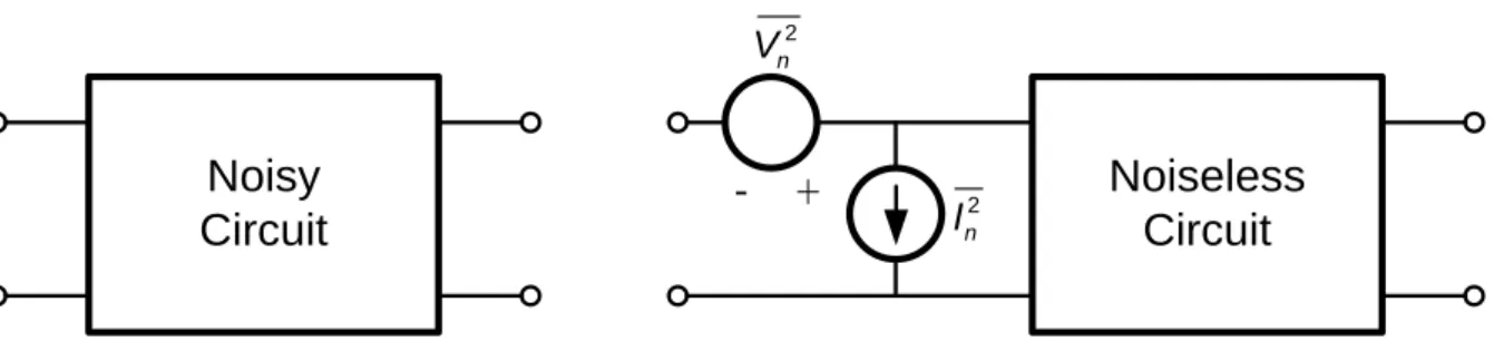
As shown in Fig. 2.8, the noise of a two-port system can be modeled by two input noise generators: a series voltage source and a parallel current source. Sometimes, this representation of noise can help us to analyze noise clear.
10
Noisy
Circuit
Noiseless
Circuit
- +
2 n I 2 n VFigure 2.8 Representation of noise by input noise generators.
2.2.4
Noise Figure
In many analog circuits, the signal-to-noise ratio (SNR), defined as the ratio of the signal power to the total noise power, is an important parameter. In RF design, most of the front-end receiver blocks are characterized in terms of their “noise figure” rather than the input-referred noise. This is partly for computational convenience and partly from tradition.
Noise figure has been defined in a number of different ways. The most commonly accepted definition is in out SNR noise figure SNR (2.15)
where SNRin and SNRout are the signal-to-noise ratios measured at the input and output,
respectively. Changing the expression slightly, we have
2 2 2 2 2 , in RS V in n out V V NF A V V 2 , 2 2 n out V RS V A V 2 , 2 1 4 n out V S V A kTR (2.16) where 2 , n out
11
output noise power by the square of the voltage gain from Vin to Vout and normalize the result
to the noise of Rs.
2.2.5
Noise Figure of Cascaded Stages
Stage 1 - + 2 Stage 2 2 n I 2 2 n V - + 2 1 n I 2 1 n V 2 RS V - + in V S R L R in1
R Rout1 Rin2 Rout2
out
V
1
v
A Av2
Figure 2.9 Cascaded noisy stages.
For a cascade of stages, the overall noise figure can be obtained in terms of the NF and gain of each stage. Consider the system shown in Fig. 2.9, where NF1 and NF2 is the noise
figure of the first stage and the second stage, respectively. Note that reactive components of the impedances are nulled and Av1 and Av2 denote the unloaded voltage gain of two stages.
The total noise power at the input of the first stage can be written as
2 2 2 1 2 1 , 1 1 1 1 2 1 1 in in n in n S in n RS in S in S R R V I R R V V R R R R (2.17)The total noise power at the input of the second stage is
2 2 2 2 2 2 2 , 2 , 1 1 2 1 2 2 1 2 2 1 in in n in n in v n out in n out in in out R R V V A I R R V R R R R (2.18)Thus, the total output noise power of the cascade equals
2 2 2 2 , , 2 2 2 2 L n tot n in v L out R V V A R R (2.19)12 1 2 , 1 2 1 1 2 2 in in L v tot v v S in out in out L R R R A A A R R R R R R (2.20)
the overall noise figure is
2 2 2 2 , 2 2 , 2 1 1 4 L tot v n in v tot L out S R NF A V A R R kTR (2.21)
Using (2.17) and (2.18) and simplifying the result, we have
2
2 1 1 2 1 2 2 2 1 4 1 1 4 4 S n S n n out n tot S v S kTR I R V I R V NF kTR A kTR (2.22) where α is equal to 2 1 1 in S in R R R .The first term on the right-hand side can be identified as the NF of the first stage with respect to a source impedance RS. The second term, on the other hand, is not as straightforward. In the
special case where RS=Rin1=Rout1=Rin2, we have
2 2 2 1 2 2 1 1 4 n S n tot v S I R V NF NF A kTR 2 1 2 2 1 1 v NF NF A (2.23)where NF2 is the noise figure of the second stage with respect to a source impedance RS.
In the general case, we simplify (2.23) using the concept of “available power gain,” Ap.
This type of gain is defined as the available power at the output (the power that the circuit would deliver to a conjugate-matched load) divided by the available source power (the power that the source would deliver to a conjugate-matched circuit.) The available output power of stage 1 in Fig. 2.9 is 2 2 2 , 1 1 1 4 out av in v out P V A R (2.24)
13 2 , 4 in source av S V P R (2.25) Thus, 2 2 1 1 S p v out R A A R (2.26) We can write (2.23) as 2 1 1 tot p NF NF NF A (2.27)
Similarly, for m stages,
2 1 1 1 1 1 1 1 1 m tot p p p m NF NF NF NF A A A (2.28)where the NF of each stage is calculated with respect to the source impedance driving that stage. This is called the Friis equation [4]. The Friis equation indicates that the noise contributed by each stage decreases as the gain preceding the stage increases, implying that the first few stages in a cascade are the most critical.
2.3 Sensitivity and Dynamic Range
2.3.1
Sensitivity
The sensitivity of an RF receiver is defined as the minimum signal level that the system can detect with acceptable signal-to-noise ratio. To calculate the sensitivity, we write
in out SNR NF SNR sig RS out P P SNR (2.29)
where Psig denotes the input signal power and PRS the source resistance noise power, both per
unit bandwidth. Since the overall signal power is distributed across the channel bandwidth, B, the (2.29) must be integrated over the bandwidth to obtain the total mean square power. Thus,
14
for a flat channel,
,
sig tot RS out
P P NF SNR B (2.30)
Assuming conjugate matching at the input, we obtain PRS as the noise power that RS delivers
to the receiver: 4 1 4 S RS in kTR P R kT 174 dBm Hz (2.31)
at room temperature. Expressing the quantities in dB or dBm, we thus simplify (2.30) as
.min 174 10log min
in dB dB
P dBm Hz NF B SNR (2.32)
Note that the sum of the first three terms is the total integrated noise of the system and is sometimes called the “noise floor”.
2.3.2
Spurious-Free Dynamic range (SFDR)
Dynamic range (DR) is generally defined as the ratio of the maximum input level that the circuit can tolerate to the minimum input level at which the circuit provides a reasonable signal quality. This definition is quantified in different applications differently. In RF design, on the other hand, the situation is more complicated. We base the definition of the upper end of the dynamic range on the inter-modulation behavior and the lower end on the sensitivity. Such a definition is called the “spurious-free dynamic range” (SFDR).
The upper end of the dynamic range is defined as the maximum input level in a two-tone test for which the third-order IM products do not exceed the noise floor. Expressing all of the quantities in dBm, we can rewrite (2.10) as
, 3 2 out IM out IIP in P P P P (2.33) where PIM,out denotes the power of IM3 components at the output. Since Pout=Pin+G and
15
of the IM3 products, we have
3 , 2 in IM in IIP in P P P P , 3 2 Pin PIM in (2.34) and hence 3 , 2 3 IIP IM in in P P P (2.35)
The input level for which IM products become equal to the noise floor is thus given by
3 ,max 2 3 IP in P F P (2.36) where F = -174dBm+NF+10log B.
The SFDR is the difference (in dB) between Pin,max and Pin,min:
3 min 2 3 PIIP F SFDR F SNR
3
min 2 3 PIIP F SNR (2.37)The SFDR represents the maximum relative level of interferers that a receiver can tolerate while producing an acceptable signal quality from a small input level.
SFDR Noise floor 3 IIP 3 OIP
16
2.4 Topologies Low Noise Amplifiers
In RF circuit design, the input and output matching is an important parameters, which indicate that how many power is reflected. When the amplifier of our design is the first gain stage in the receive path, not only impedance matching but also noise figure is significant consideration, since its noise figure directly adds to that of the system. In this subsection, we will introduce six input matching architectures.
2.4.1
Input Matching
A. Resistive termination L R p R S R in V out VFigure 2.11 Common-source amplifier with shunt input resistor.
One straightforward approach to providing a reasonably broadband 50 Ohm termination is simply to put a 50 Ohm resistor across the input terminals of a common-source amplifier. In Fig. 2.11, a 50 Ohm resistor is placed in parallel with the input, and the capacitive part of input impedance is canceled by an external inductor.
The termination resistor, however, generates noise as well. In fact, the noise figure of a stage consisting of a parallel resistor Rp with respect to a source resistance RS is
4 1 S p m S R NF R g R (2.38)
17
where α=gm/gd0.
Unfortunately, the resistor Rp adds thermal noise of its own, and attenuates the signal ahead of
the transistor. The combination of these two effects generally produces unacceptably high noise figure. For Rp=RS, the noise figure of the LNA exceeds 3dB. The key point here is that
the circuit must exhibit a 50 Ohm input resistance without the thermal noise of a 50 Ohm resistor.
B. Resistive shunt feedback
out V L R F R in Z in V S R
Figure 2.12 Resistive shunt feedback.
The circuit topology of a resistive shunt feedback LNA is shown in Fig. 2.12, which can provide a broadband input matching. The input impedance can be derived as
1 1 1 1 F L in m L R R Z g R (2.39)
The resistive feedback network continues to generate thermal noise of its own. The noise figure can be derived as
2 2 2 1 1 1 1 1 1 1 1 1 1 1 1 1 1 1 S S m S F m F S S L S m F m m F F F R R g R R g R NF R R R R g R g g R R R (2.40)
18
As a consequence, this topology typically requires larger power consumption or more advanced technologies to achieve an acceptable NF. This is primarily due to the inherently low transconductance of CMOS, which not only degrades the noise performance but also prohibits the use of a large feedback resistor.
C. Common Gate L R S R in V out V in Z
Figure 2.13 Common-gate stage.
Figure 2.13 depicts a common-gate stage designed to exhibit an input resistance of 50 Ohm; that is, 1/(gm+gmb)=50 Ohm. The input capacitance may be nulled by means of an
external inductor. With the input impedance matched to 50 Ohm, its noise figure NF is derived as 1 4 1 S L R NF R (2.41)
The principal drawback of this topology is that the transconductance of the input transistor cannot be arbitrarily high, thus imposing a lower bound on the noise figure. The noise figure will be significantly worse at high frequencies and when gate current noise is taken into account.
19
D. Inductive degeneration
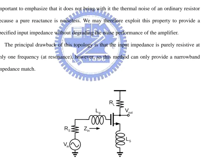
Another topology of creating an input resistance of 50 Ohm is illustrated in Fig. 2.14. Neglecting the gate-drain and source-bulk capacitance, we can write
1 m S in S g gs gs g L Z s L L C sC (2.42)The inductance LS is chosen to provide the desired input resistance (equal to RS, the source
resistance). Since the input impedance is purely resistive only at resonance, an additional degree of freedom, provided by inductance Lg, is needed to guarantee this condition. An
important advantage of this method is that one then has control over the value of the real part of impedance through choice of inductance. Whatever the value of this resistive term, it is important to emphasize that it does not bring with it the thermal noise of an ordinary resistor because a pure reactance is noiseless. We may therefore exploit this property to provide a specified input impedance without degrading the noise performance of the amplifier.
The principal drawback of this topology is that the input impedance is purely resistive at only one frequency (at resonance), however, so this method can only provide a narrowband impedance match. S R in V out V L R S L g L in Z
20
E. Multistage input filter
As shown in Fig. 2.15, this topology is to use a multistage input filter for broadband input matching. Although this filter-type topology achieves broadband matching and low power consumption, the input filter insertion loss degrades the amplifier’s noise performance, and this loss must be compensated for by increasing the gain, thereby lowering bandwidth. In addition, this topology requires a large number of high-Q inductors at the input, making it difficult to realize them in a small chip area.
L R S R in V out V Broadband LC-filter S L
Figure 2.15 Multistage input filter.
F. Distributed amplifier
The basic distributed amplifier is shown in Fig. 2.16. The input impedance matching is achieved by designing the characteristic impedance of transmission line, Zo L C , g g equal to the source impedance, RS, usually 50 Ohm. To avoid unwanted reflection from the
transmission line, the gate-termination resistor, Rg is also set equal to the characteristic
impedance, Zo.
The distributed amplifier provides good impedance matching and flat gain over a wide range of frequencies. However, the demand for high-quality transmission lines makes them
21
less attractive to low-cost applications because of the larger chip area and higher power consumption. S R in V out V g R L2 R L1 R 1 M M2 Mn
Figure 2.16 Basic distributed amplifier.
2.4.2
Summary
The summary of six input matching architectures is listed in Table I. The resistive termination provides good input matching but the resistor increases noise figure. The resistive shunt feedback provides wide band input matching but increases noise figure due to the local feedback resistor. The common-gate stage also provides wide band input matching. However, lower bound on the noise figure is restricted by lower transconductance. The inductive degeneration can only provide a narrowband input matching but it can achieve better noise performance. The multistage input filter topology provides broadband matching and low power consumption but insertion loss degrades the noise performance. Finally, the distributed amplifier provides good wideband input matching and flat gain. However, it consumes more power and chip area.
22
Table I
Six input matching architectures summary
L R p R S R in V out V L R S R in V out V in Z
(a) Resistive termination. Resistor degrade the noise figure.
(b) Common-gate stage. Lower bound on noise figure.
out V L R F R in Z in V S R S R in V out V L R S L g L in Z
(c) Resistive shunt feedback Broadband but higher power consumption.
(d) Inductive degeneration Narrow band but can achieve better noise
performance. L R S R in V out V Broadband LC-filter S L S R in V out V g R L2 R L1 R 1 M M2 Mn
(e) Multistage input filter
Broadband but insertion loss degrade noise performance with large chip area.
(f) Distributed amplifier
Broadband and flat gain but large chip area with high power consumption.
23
2.5 Bandwidth Techniques
The bandwidth enhancement is achieved by shunt peaking, a method first used in the 1940’s to extend the bandwidth of television tubes. We first describe the fundamentals of this approach. Then we will introduce a triple-resonance architecture.
2.5.1
Shunt Peaking
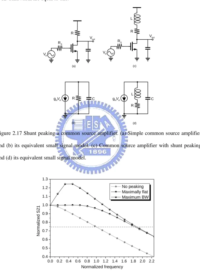
Although inductors are commonly associated with narrow-band circuits, they are useful in broadband circuits as well. In this section, we study how an inductor can enhance the bandwidth of a broadband amplifier [5].
We consider the simple common source amplifier illustrated in Fig. 2.17. For simplicity, we assume that the small signal frequency response of this amplifier is determined by a single dominant pole, which is determined solely by the output load resistance R and the load capacitance C [see Fig. 2.17(b)].
1 out m in V g R V j RC (2.43)The introduction of an inductance L in series with the load resistance alters the frequency response of the amplifier [Fig. 2.17(c)]. This technique, called shunt peaking, enhances the bandwidth of the amplifier by transforming the frequency response from that of a single pole to one with two poles and a zero [Fig. 2.17(d)].
2
1 m out in g R j L V V j RC LC (2.44)The zero is determined solely by the L/R time constant and is primarily responsible for the bandwidth enhancement. The frequency response of this shunt peaked amplifier is characterized by the ratio of the L/R and RC time constants. This ratio is denoted by m so that L=mR2C.
24
The case with no shunt peaking is used as the reference so that its low-frequency gain and its 3-dB bandwidth are equal to one.
R S R in V out V R S R in V out V m gVin R L C m gVin R C (a) (b) (c) (d) L
Figure 2.17 Shunt peaking a common source amplifier. (a) Simple common source amplifier and (b) its equivalent small signal model. (c) Common source amplifier with shunt peaking and (d) its equivalent small signal model.
0.0 0.2 0.4 0.6 0.8 1.0 1.2 1.4 1.6 1.8 2.0 2.2 0.4 0.5 0.6 0.7 0.8 0.9 1.0 1.1 1.2 1.3 N orm aliz ed S21 Normalized frequency No peaking Maximally flat Maximum BW
25
2.5.2
Triple-Resonance Architecture
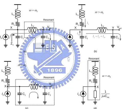
To arrive at the concept of the triple-resonance amplifier (TRA) [6], first consider the inductively peaked cascade of two stages shown in Fig. 2.19(a), where it is assumed that M1
and M2 contribute approximately equal capacitance (C/2) to node X. As the frequency
approaches 1 1 1 L C (2.45)
the impedance of L1 rises, allowing a greater fraction of ID1 to flow through C1+C2 and hence
extend the bandwidth.
To increase the bandwidth, we insert an inductor L2 in series with C2 [Fig. 2.19(b)] such
that L2 and C2 resonate at ω1, thereby acting as a short and absorbing all of ID1. Now, ID1 flows
through C2 rather than C1+C2, leading to a more gradual roll-off of gain. For L2 and C2 to
resonate at ω1, we have L2=2L1. Since, in practice, C1 and C2 are not exactly equal, the ratio of
L1 and L2 can be adjusted to compensate for this difference. To minimize peaking, the output
voltage at this frequency Iin/(C2ω1) must be equal to that at low frequencies IinR1, yielding
1 1 2 L R C (2.46)
The series resonance of L2 and C2 depicted in Fig. 2.20(a) not only forces all of Iin to flow
through C2, but reverses the sign of the impedance Zx, thus making Vx negative for ω>ω1. As
illustrated in Fig. 2.20(b), I1 and I2 must therefore flow into node X and, together with Iin, pass
through C2. Consequently, |Vout/Iin| continues to rise until the π network consisting of C1, L2,
and C2 begins to resonate [Fig. 2.20(c)], presenting an infinitely impedance at node X and
allowing all of Iin to flow through R1 and L1. For ω>ω2, the π network becomes capacitive and
|Vout/Iin| begins to fall, returning to the mid-band value R1 when the impedance of the π
network resonates with L1 [Fig 2.20(d)]. The amplifier exhibits the frequency response shown
26 (a) (b) 1 R in V 1 L 1 C C2 1 M X 2 M 1 R in V 1 L 1 C C2 1 M X L2 Y 2 M
Figure 2.19 (a) Inductively peaked stage, (b) TRA.
(a) 1 R 1 L 1 C C2 X L2 Y in I out V 1 R 1 L 1 C C2 X L2 Y in I out V Resonant 1 x Z 1 2 in I I I 1 I 2 I 1 (c) 1 R 1 L 1 C C2 X 2 L in I out V Resonant 2 (d) 1 R 1 L eq 1 C j X in I Resonant 3 (b)
Figure 2.20 Behavior of a triple-resonance circuit at different frequencies.
1 R 1 out D V I 1 2 3
27
Chapter 3 Design of Parallel-RC feedback UWB LNA
The challenge of building a single radio frequency front-end capable of receiving and processing a multiplicity of bands has stimulated interest in broadband RFIC design. As discussion in section 2.4, the resistive shunt feedback suffers high noise figure and the inductive degeneration can only provides narrow band. To solve these problems and combine the advantages of them, a CMOS UWB LNA with low noise figure, small chip area, and higher figure of merit (FoM) is presented.
Output buffer Second stage Input stage L1 R DD V VDD VDD S R in V F R F C D1 C D1 L D2 L L2 R S1 L G1 V B1 R B2 R 1 M M2 3 M 4 M out V
28
3.1 Circuit Design and Analysis
The proposed UWB LNA is depicted in Fig. 3.1. It consists of an input stage, a casecode second stage, and an output buffer. We will discuss their function in order.
3.1.1
Input Stage
(a) (b) in Z in Z , F R C,F , F R C,F , in Z , in Z p R Cp Lp S1 L 1 MFigure 3.2 (a) Miller equivalent circuit. (b) series converted to parallel of equivalent circuit.
The input stage provides the broadband power and noise matching. The input impedance Z’in seen looking into the gate of transistor M1 is [2]
, 1 1 1 1 1 1 S in m S gs gs L Z g sL C sC (3.1) where gm1 and Cgs1 is the transconductance and the gate-to-source capacitance of the transistor
M1, respectively. From Fig. 3.1, using Miller’s theorem to convert the input stage to that
shown in Fig. 3.2(a), we have RF’=RF/(1+Av) and CF’=CF(1+Av), where Av is the voltage
29
, 1 , 1 gs in m F L v gs in F L sC Z g Z Z A sC Z Z Z (3.2) Equation (3.1) presents a series-RLC network. For simplicity, the series combination of R, L, and C can be converted to the equivalent parallel circuit shown in Fig. 3.2(b), where Rp, Lp,and Cp can be derived as
2 2 1 p R L C R R (3.3)
2 2 2 1 p R L C L L (3.4)
2
2 2 1 1 p C C R L C (3.5)Thus, the input impedance Zin can be derived as
,
, 1 in F p p F p Z R R sL s C C (3.6) Referring to (3.6), we can make the following observations. First, the form of (3.6) clearly shows that the input impedance is purely resistive at resonance. Thus, a proper choice of gm1,LS1, RF, and CF yields a 50 Ω real part. In (3.6), CF makes the capacitive reactance of Zin
closer to the inductive reactance. In other words, CF makes the imaginary part of Zin closer to
zero (see Fig 3.3). Thus, Zin is dominated by RF’∥Rp during several gigahertz. As a result, the
optimal choice of gm1, LS1, RF, and CF ensures broadband input matching condition. Second,
the resistive component at the input is the parallel combination of RF’ and Rp, and the local
feedback noise is inversely proportional to RF; hence we can select larger feedback resistor RF
in order to suppress noise. The effect of RF on NF is shown in Fig. 3.4. Third, different from
the conventional inductive degeneration [7], the design in this study only uses a small inductor LS1 for input matching, so the core area can be reduced.
30 3 4 5 6 7 8 9 10 11 -40 -35 -30 -25 -20 -15 -10 -5 0 5 Im {Z in} (Ohm ) Frequency (GHz) wi CF wo C F
Figure 3.3 Effect of CF on input impedance.
3 4 5 6 7 8 9 10 11 2.0 2.5 3.0 3.5 4.0 N F (dB) Frequency (GHz) R F= 3kΩ R F= 2kΩ RF= 1kΩ R F= 500Ω R F= 300Ω Figure 3.4 Effect of RF on NF.
31
From the above observations, the proposed input stage has combined the advantages of the resistive feedback and the inductive degeneration and can provide wide-band input matching and better noise performance with a relatively small area. Moreover, a general noise figure of common-source amplifier is linearly proportional to the frequency in 3-10 GHz. The noise factor of input stage Fin is equal to
2 , 1 2 1 4 n o in v S V F A kTR (3.7) where Vn,o1 represents the total noise at output of input stage, which includes the thermal noise
of RS, RF, RL1, and M1. From Fig. 3.2(a) the noise contributed by RS, RF, and M1 is
proportional to Av, so RL1 plays a critical role in increasing Fin due to low Av at high frequency.
Thus we suppress the high-frequency noise of RL1 to maintain low NF. As depicted in Fig. 3.5,
we assume that the impedance seen looking into the drain of M1 is equal to Zo, the impedance
of parallel-LC circuit is ZLC,and the output noise voltage contributed by RL1 can be derived as
2 2 , 1 1 2 1 4 o n o L o L LC Z V kTR Z R Z (3.8)From (3.8) the Vn,o1 is inversely proportional to ZLC, so the output noise voltage can be
effectively reduced at resonance. As shown in Fig. 3.6, the LD1, CD1, and LS1 can reduce
high-frequency noise (7- 15GHz) effectively.
+ -D1 L CD1 L1 R LC Z S1 L o Z Vn,o1 L1 n,R V 1 M F R F C S R
32 2 4 6 8 10 12 14 16 0.0 0.5 1.0 1.5 2.0 2.5 3.0 3.5 4.0 4.5 5.0 wi L DCDLS1 wo L DCDLS1 Z LC Frequency (GHz) N F (dB) 200 400 600 800 1000 1200 1400 1600 Z LC (m agnit ude)
Figure 3.6 Effect of LD, CD, and LS1 on NF of input stage.
0 FBB Non-FBB G D S B FBB Non-FBB D I t1 V t2 V VGS B V
Figure 3.7 I-V characteristics of MOSFET with and without FBB.
3.1.2
Second Stage
The second stage is a cascode common-source stage, which provides high-frequency gain and better isolation. The transistor M3 is used for improvement of M1’s Miller effect, better
isolation, and higher gain. The series peaking inductor LD2 can resonate with the total parasitic
capacitances CD3 at the drain of M3, and a resistor RD2 is added to reduce Q factor of LD2 for
33
For deep-submicrometer MOSFETs, the threshold voltage Vt is no longer constant, but
influenced by circuit parameters such as gate length, channel width, and drain-to-source voltage due to the short-channel and narrow-channel effects [8]. Typically, transistors with a large channel width and a minimum gate length exhibit a reduced Vt, which is preferable for
low-voltage operations. For a MOSFET device, the threshold voltage is governed by the body effect as
0 2 2 2 t t A S ox F SB F V V qN C V (3.9) where Vt0 is the threshold voltage for VSB=0, ϕ F is a physical parameter with a typical value of0.3 V, NA is the substrate doping, and εS is the permittivity of silicon. From (3.9) we can know
that by applying a forward body bias (FBB) technology (see Fig. 3.7), the effective threshold voltage is thus reduced while maintaining a minimum forward junction current between the body and the source terminals.
As shown in Fig. 3.1, we use a voltage divider which consists of resistors RB1 and RB2 to
achieve the Forward Body Bias technique [8]. A general FBB needs an extra DC bias. In other words, we can save an extra DC pad by using a voltage divider, therefore the complexity of layout is lessened; and the FBB can further obtain same gm2 with a low supply voltage so that
the power consumption can be reduced. Finally, Fig. 3.8 shows simulation frequency response of input stage, second stage, and overall stage. The input stage and the second stage provides low-frequency power gain and high-frequency power gain, respectively. The combination both frequency response results a broadband power gain.
34 0 2 4 6 8 10 12 14 -15 -10 -5 0 5 10 15 20 25 S21 (dB) Frequency (GHz) overall input second
Figure 3.8 Simulation frequency response of input stage, second stage, and overall stage.
3.1.3
Output Buffer
The output buffer is a simple source follower. The output impedance can be approximated as 1/gm, which is selected as 50 Ohm for output matching. In order to reduce the parasitic
capacitance arisen from a large device, the input device of this buffer must be reduced despite the larger loss occurs. The fixed bias current for M4 is 4.4 mA from 1.4-V supply.
3.1.4
Noise Analysis
The noise figure of the proposed LNA is dominated by M1, RF, and RL1 and can be derived
as
2 2 , , 1 1 2 2 , , , 1 1 m L F S in L in gs M v S m L S in F S in L in gs g Z Z R Z Z Z sC F A R g Z R Z Z R Z Z Z sC (3.10)
2 2 , , 1 2 2 2 , , , 1 1 1 F L m S in in gs RF v S F F S in m L L F S in in gs R Z g R Z Z sC F A R sC R R Z g Z Z Z R Z Z sC (3.11)
2 1 1 2 2 1 o L RL v S LC L o Z R F A R Z R Z (3.12)35 where Zo is defined by
, , 1 , 1 F S in in gs o m S in Z R Z Z sC Z g R Z (3.13)Thus, the total noise factor F is approximated as
1 1
1 M RF RL
F F F F (3.14)
In Equation (3.11) and (3.12), the FRF and the FRL1 is inversely proportional to RF and ZLC,
respectively. As a result, a larger feedback resistor RF and a parallel-LC network can suppress
noise effectively. L1 R DD V S R in V F R F C D1 C D1 L S1 L 1 M n,o1 V , 1 n M I , 1 n RL V , n RF V + -+
-Figure 3.9 Noise equivalent circuit of input stage.
3.2 Experimental Results
The proposed UWB LNA has been fabricated by the TSMC 0.18-μm CMOS process. The chip microphotograph is shown in Fig. 3.10. The chip area is 0.697 mm × 0.657 mm including testing pads. The measurement is carried out on wafer for RF characterization.
Fig. 3.11 shows measured and simulated power gain and input return loss of the UWB LNA. The measured power gain is 12.4 dB (±1.5 dB variation) over 3.1 to 10.6 GHz. The measured high-frequency gain is less than simulated one about 1.4 dB. It may be due to
36
process variation and inaccuracy of inductor and transistor models. The measured input return loss is -9.4 to -32.5 dB from 3.1 to 15GHz. Fig. 3.12 shows measured and simulated output return loss and reverse isolation of the UWB LNA. The measured output return loss is below -8.5 dB and the measured reverse isolation is below -45 dB across the entire band.
The measured and simulated NFs are illustrated in Fig. 3.13. The measured NF is 2.5-4.7 dB from 3.1 to 10.6 GHz. The measured NF is larger than the simulated one due to degraded power gain. Fig. 3.14 shows IIP3 measured by applying two-tone test with 1-MHz spacing. The measured IIP3 is -8.5 dBm at 8 GHz.
In general, the figure of merit (FoM) is applied to evaluate performance of LNAs, and is defined as [9]
21
1 1 1 1 DC t S BW GHz FoM mW NF P mW f GHzThis FoM includes the most relevant parameters in order to evaluate a UWB LNA for low-cost and low-power applications.
37 0 2 4 6 8 10 12 14 -40 -35 -30 -25 -20 -15 -10 -5 0 5 10 15 20 25 S21, S11 (dB) Frequency (GHz) measured S21 measured S11 simulated S21 simulated S11
Figure 3.11 Measured and simulated power gain (S21) and input return loss (S11) of the UWB LNA. 0 2 4 6 8 10 12 14 -90 -80 -70 -60 -50 -40 -30 -20 -10 0 S22, S12 (dB) Frequency (GHz) measured S22 measured S12 simulated S22 simulated S12
Figure 3.12 Measured and simulated output return loss (S22) and reverse isolation (S12) of the UWB LNA.
38 3 4 5 6 7 8 9 10 11 12 0 1 2 3 4 5 6 N F (dB) Frequency (GHz) measured NF simulated NF
Figure 3.13 Measured and simulated noise figure of the UWB LNA.
-40 -35 -30 -25 -20 -15 -10 -5 -110 -100 -90 -80 -70 -60 -50 -40 -30 -20 -10 0 Out put Pow er (dBm ) Input Power (dBm) Fundamental tone IM3 tone IIP3= -8.5dBm
39
TABLEII
Measured Performance Summary and Comparison
Ref. CMOS Technology BW3-dB (GHz) Gmax (dB) NF (dB) IIP3 (dBm) Power (mW) Area (mm2) FoM (W-1) This Work 0.18μm 3.1-10.6 13.9 2.5-4.7 -8.5 14.4 0.46 57.1 [1] 0.18μm 1.2-11.9 9.7 4.5-5.1 -6.2 20 0.59 15.5 [3]STD 0.18μm 2.3-9.2 9.3 4-8 -6.7 9 1.1 25.5 [10] 0.18μm 0.4-10 12.4 4.4-6.5 -6 12 0.42 32.8 [11]+ 0.18μm 3.1-10.6 17.5 3.1-5.7 - 33.2* 0.5 28.2 [12] 0.18μm 2.8-7.2 19.1 3-3.8 -1 32* 1.63 21.5 [13] 0.18μm 0.04-7 8.6 4.2-6.2 +3 9 1.16 22.1 +:Simulation only.
*:The power consumption including buffer, ours is 21mW.
3.3 Summary
A UWB LNA is proposed and implemented by the TSMC 0.18-μm 1P6M process. The measured performance of the proposed LNA is compared with others, which is summarized in Table II. It is found that our circuit achieves the lowest noise figure and the best FoM. The proposed UWB LNA compared with other UWB techniques has excellent noise performance, small size, and higher FoM.
40
Chapter 4 Design of Noise-Canceling UWB LNA
Since the LNA is the first gain stage in the receive path, its noise figure directly adds to that of the system. As discussed in section 2.4, we suppress noise of LNA as much as possible in order to obtain better SFDR. In this chapter, we use a transformer to achieve noise cancellation with low power consumption and realize in UWB frequency.
4.1 Noise-Canceling Principle
Vsignal 3 M 1 M 2 M L1 R S R n,M1 I n,out I 0 X Y41
The purpose of noise cancellation is to decouple the input matching with NF by canceling the output noise from the matching device. Fig. 4.1 illustrates an example, which is based on a common-gate LNA. The input matching is accomplished by setting 1/gm1 to 50 Ω. The noise
current of M1 is modeled by the current source In,M1, which flows into node X but out of node
Y. This creates two fully correlated noise voltages at nodes X and Y with opposite phases. These two voltages are converted to currents by M3 and M2, respectively. By properly
designing gm2 and gm3, the noise contributed by M1 can be cancelled at the output. On the
other hand, the signal voltages at nodes X and Y are in phase, resulting in constructive addition at the output. The condition for complete noise cancellation is derived as [1]
, 1 , 1 , 1 2 3 1 1 0 1 1 n M n M n out L m S m m S m S I I I R g R g g R g R 2 1 3 g Rm L g Rm S (4.1)
Although the noise contributed by M1 can be cancelled at the output, another input device M3
is still contributed noise to the output. Thus, the noise of the whole system is difficult to be reduced to a very low level.
According to the points discussed above, by using a transformer to achieve noise cancellation is proposed. An initially noise-canceling topology is depicted in Fig. 4.2. We will be divided into signal and noise two parts and analyzed the noise-canceling principle. As shown in Fig. 4.2(a), the input signal at gate of transistor M1 can produce an opposite-phase
signal at drain of transistor M1. The transformer induces an opposite-phase signal at source of
M1. Consequently, the signals at source and drain of M1 can be amplified and added to the
output via M2 and M3, respectively. As shown in Fig. 4.2(b), the noise current of M1 is
modeled by the current source In,M1 which flows into node X but out of node Y. This produces
two fully correlated noise voltages at nodes X and Y with opposite phases. These two voltages are converted to currents by M2 and M3, respectively. We assume that the impedance at drain
42
, , 1 2 3
n out n M D m S m
I I Z g Z g (4.2) Thus, the condition for complete noise cancellation is
2 3
D m S m
Z g Z g (4.3) The proposed noise-canceling technique does not have noise source contributed by another input device, so we can be in order to expect its noise is suppressed effectively.
+ = Vsignal (a) (b) 1 M 2 M 3 M g V out V in V 1 M 2 M 3 M g V in V Vout n,out I 0 n,M1 I X Y
43
4.2 Circuit Design of The Noise-Canceling UWB LNA
S R in V DD V DD V DD V g V 1 T 1 M 2 M 3 M 2 L D1 R D2 R 1 L 3 L 4 M L3 R out V
Figure 4.3 Proposed noise-canceling UWB LNA.
The proposed noise-canceling UWB LNA is depicted in Fig. 4.3. The inductor L1 is used
for shunt peaking, extending the bandwidth efficiently. The input capacitance of M3 influences
inductance of transformer to bring unnecessary resonance. In order to lighten this problem we use a series inductor L2 at source of M3. Thus, the equivalent input capacitance of M3 is
reduced. The series inductor L3 further resonates with the input capacitance of M4, resulting in
a large bandwidth. An output matching stage which consists of transistor M4 and resistor RL3