Structural and optoelectronic properties of GZO/SiOx bilayer films by
atmosphere pressure plasma jet
Kow-Ming Changa,b, Po-Ching Hoa, Chi-Wei Wua, Chin-Jyi Wuc, Chia-Chiang Changc a Department of Electronics Engineering & Institute of Electronics, National Chiao Tung
University, 1001 Ta Hsueh Road, Hsinchu, Taiwan 30010, R.O.C.
b College of Electrical and Information Engineering, I-Shou University, No.1, Sec. 1, Syuecheng Rd., Dashu Township, Kaohsiung County, Taiwan 84001, R.O.C. c Industrial Technology Research Institute, Mechanical and Systems Research
Laboratories, Hsinchu, Taiwan 310, R.O.C.
Using simple technique to obtain high haze and high conductivity TCO films to enhance optical absorption for silicon thin film solar cell is important. The bilayer GZO film of high haze and low resistivity is achieved by atmosphere pressure plasma jet (APPJ). Thickness of bilayer GZO film was thinner than Asahi-U type FTO film and this result indicated that the APPJ deposition technique has lower material comsumption. The minimum resistivity of 6.00×10⁻⁴ was achieved at 8 at% gallium doping. X-ray diffraction spectrum showed that an increase in scanning times led to an increase in crystallinity of bilayer GZO films. The bilayer GZO film has much higher haze value in the visible and NIR regions as compared to Asahi U-type FTO film.
Introduction
Transparent conductive oxide (TCO) has attracted substantial attention due to its widely applications, such as solar cells (1-3), flat-panel displays and light emitting diodes. Inside the silicon thin film solar cell, amorphous silicon (a-Si) and microcrystalline silicon (μc-Si) thin films are two important absorber materials. Owing to reducing light-induced degradation, the a-Si thin film should be deposited as thin as possible. The μc-Si thin film is indirect and has low absorption coefficient, so the thickness of it should be deposited thick enough to completely absorb sunlight during single path. In order to fulfil above requirements, it is necessary for development of high haze and high conductivity of the TCO coatings to enhance optical absorption in terms of light trapping (4-7). Using simple technique to obtain high haze and high conductivity TCO films is important. However, the manufacturing processes of commercial Asahi U-type (SnO2:F) TCO glass demand high deposition temperature and use expensive toxic gas. This study develops the TCO films by the atmosphere pressure plasma jet (APPJ). Several advantages of the APPJ deposition system include low cost, low temperature processes and application in large area applications (8). The influence of physical properties of SiOx on the growth of GZO films was investigated.
Experimental
In this study, silicon suboxide (SiOx) was used as buffer layer to increase light scattering ability of GZO films. After the SiOx buffer layer was deposited on glass, the
625W and substrate temperature was fixed at 150 C. The flow rates of N2 carrier gas and main gas were fixed at 300 sccm and 35 SLM, individually. Scanning number of APPJ was varied as 10, 15 and 20 times owing to obtaining optimal GZO film.
Surface morphologies and thicknesses of SiOx buffer layers and GZO films were analyzed by scanning electron microscope (SEM). The roughness was determined by a DI Digital DI-D3000 atomic force microscopy (AFM). Electrical properties of GZO films were analyzed by Hall measurement. The optical transmittance and haze values were measured by using UV-vis-NIR spectrophotometer. Grazing incidence X-ray diffraction (GIXRD) spectrum of GZO films were measured using x-ray diffractometer.
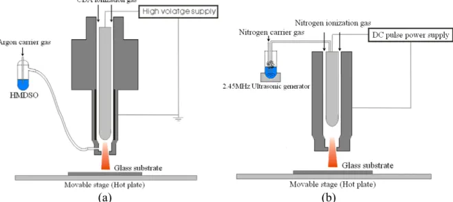
(a) (b)
Figure 1. Schematic diagram of the experimental equipment for (a)SiOx (b)GZO.
Results and Discussion
SiOx buffer layer effect
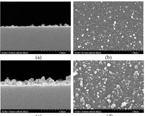
Figure 2 shows surface and cross-sectional SEM images of SiOx buffer layers deposited for different argon carrier gas flow rates, 30 and 60sccm. At flow rates of argon carrier gas, 30 and 60 sccm, thicknesses of SiOx thin films were 20 and 36 nm, respectively. Root mean square (RMS) roughnesses of the SiOx buffer layers deposited at argon carrier gas flow rates of 30 and 60 sccm, were 12.20 and 34.87 nm, respectively. Thicknesses and RMS roughness of SiOx thin films increase as argon carrier gas flow rates increase.
(a) (b)
(c) (d)
Figure 2. Cross-sectional and surface SEM images of SiOx buffer layers deposited by using different Ar carrier gas flow rate (a,b)30sccm (RMS=12.20nm) (c,d)60sccm (RMS=34.87nm).
Figure 3 dipics transmittance and haze spectra of conventional GZO film and bilayer GZO films using SiOx as buffer layers, which were deposited at argon carrier gas flow rates of 30 and 60 sccm. With the increase in argon carrier gas flow rates, transmittance of bilayer GZO films decreased because of thicker SiOx buffer layer, as shown in Fig. 3a. Figure 3b shows haze values of bilayer GZO films in visible region have a significant increase compared with conventional GZO.
(a) (b)
Figure 3. (a)Transmittance and (b) haze spectra of conventional GZO film and bilayer GZO films deposited on SiOx buffer layers for different carrier flow rates. Conventional GZO film and bilayer GZO films were scanned 20 times by APPJ.
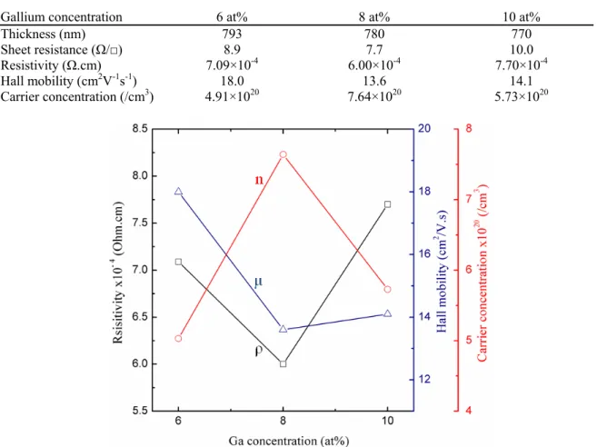
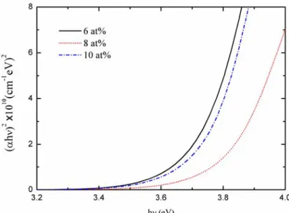
bilayer GZO films for different Ga concentration are summarized in Table I. The plots of (αhν)2 versus photon energy of bilayer GZO films deposited for different Ga/(Zn+Ga) atomic ratios, as shown in Fig. 5. Table II shows optical bandgap of bilayer GZO films for Ga doping concentration from 6 at% to 10 at%. According to Burnstein-Moss effect, the optical bandgap increased with an increase in carrier concentration. The maximum optical bandgap of 3.82 eV was achieved at approximately 8 at% gallium doping. The result is consistent with carrier concentration measured by Hall measurement, as shown in Table I. It is interesting to note that a decrease of optical bandgap is observed at 10 at%.
Table I. Electrical properties of bilayer GZO films scanned 20 times for different Ga concentration.
Gallium concentration 6 at% 8 at% 10 at%
Thickness (nm) 793 780 770
Sheet resistance (Ω/□) 8.9 7.7 10.0
Resistivity (Ω.cm) 7.09×10⁻⁴ 6.00×10⁻⁴ 7.70×10⁻⁴
Hall mobility (cm2V-1s-1) 18.0 13.6 14.1
Carrier concentration (/cm3) 4.91×10²⁰ 7.64×10²⁰ 5.73×10²⁰
Figure 4. Resistivity (ρ), Hall mobility (μ) and carrier concentration (n) of bilayer GZO films deposited for different Ga/(Zn+Ga) atomic ratios.
Figure 5. The plots of (αhν)2 versus photon energy of bilayer GZO films deposited for different Ga/(Zn+Ga) atomic ratios.
Table II. Optical bandgap of bilayer GZO films scanned 20 times for different Ga doping concentration.
Gallium concentration 6 at% 8 at% 10 at%
Optical bandgap (eV) 3.71 3.82 3.74
Scanning times effect
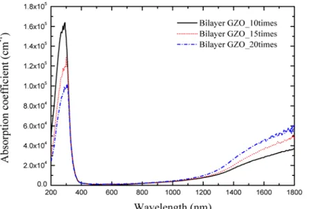
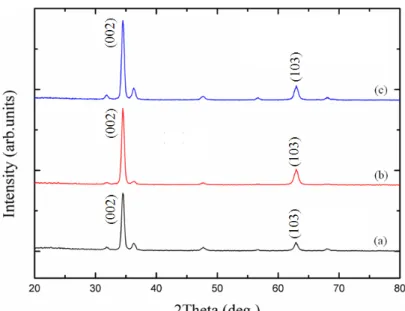
Figure 6 shows cross-sectional and surface SEM images of bilayer GZO films, which were scanned 10, 15 and 20 times by APPJ. SiOx buffer layers deposited at argon carrier gas flow rates of 30 sccm and were scanned 1 times by APPJ. Thicknesses of bilayer GZO films measured by SEM were 450, 630 and 780nm for 10, 15 and 20 times, respectively. Owing to different flow rates between main gas and carrier gas, vortex was formed inside tube, which caused radicals have a long resident time, and resulted in formation of particles (10). As number of scans increase, bilayer GZO films shows thicker films, rougher surface morphologies and larger grain size. Figure 7 dipics absorption coefficient spectra of bilayer GZO for different scanning times, 10, 15 and 20times. In the ultraviolet region, the absorption coefficients decrease with an increase of Ga doping concentration (11). It can be speculated increasing scanning times could increase Ga/(Zn+Ga) atomic ratios. Figure 8 displays GIXRD patterns of bilayer GZO for different scanning times, 10, 15 and 20times. All bilayer GZO films exhibit preferred orientation along (002) plane. An increase in scanning times led to an increase in intensity of (002) peaks, as can be confirmed from Fig. 8. This results indicate a significant increase in crystallinity of bilayer GZO films. It worth noting that the ionic radius of Ga is smaller than Zn. Gallium incorporation caused lower lattice constant (12). There was a positive correlation between the lattice constant and d spacing. The Bragg angle was determined from d spacing. The positive shift in 2theta values of (002) peaks for bilayer GZO films resulted from increment of Ga doping concentration.
(b) (e)
(c) (f)
Figure 6. Cross-sectional and surface SEM images of bilayer GZO film scanned (a,d)10 times (b,e)15 times (c,f)20 times by APPJ. SiOx buffer layers deposited at argon carrier gas flow rates of 30 sccm and were scanned 1 times by APPJ.
Figure 7. Absorption coefficient spectra of bilayer GZO for different scanning times: (a)10times (b)15times (c)20times.
Figure 8. GIXRD patterns of bilayer GZO for different scanning times: (a)10times (b)15times (c)20times.
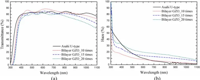
Table III compares electrical properties of Asahi U-type FTO and bilayer GZO films. The data do not show a significant increase in Hall mobility of bilayer GZO films. The resistivity of bilayer GZO film scanned 20 times was lower than Asahi U-type FTO film. This is attributed to high carrier concentration of bilayer GZO film deposited by scanning 20 times. Figure 9 shows the transmittance and haze of Asahi U-type FTO and bilayer GZO films of different number of scans, 10, 15 and 20 times. The transmittance in the 750-1100 nm region was lower than 80% for all bilayer GZO films due to high carrier concentration increasing free carrier absorption is shown in Fig. 9a. The bilayer GZO film scanned 20 times has much higher haze value in the visible and NIR regions, when compared to Asahi U-type FTO film and other bilayer GZO films, as shown in Fig. 9b.
Table III. Electrical properties of Asahi U-type FTO and bilayer GZO films.
Asahi U-type FTO Bilayer GZO
Number of scans 10 times 15 times 20 times
Thickness (nm) 900 450 630 780 RMS (nm) 33.10 27.00 32.70 40.73 Sheet resistance (Ω/□) 8.2 19 11 7.7 Resistivity (Ω.cm) 7.38×10⁻⁴ 8.55×10⁻⁴ 6.93×10⁻⁴ 6.00×10⁻⁴ Hall mobility (cm2V-1s-1) 46.2 13.1 13.2 13.6 Carrier concentration (/cm3) 1.830×10²⁰ 5.573×10²⁰ 6.823×10²⁰ 7.641×10²⁰ Table IV. Optical (at 500nm) properties of Asahi U-type FTO and bilayer GZO films.
Asahi U-type FTO Bilayer GZO
Number of scans 10 times 15 times 20 times
Transmittance (%) 83.0 84.0 83.2 81.0
(a) (b)
Figure 9. (a)Transmittance (b)haze of Asahi U-type FTO film and bilayer GZO films of different number of scans, 10, 15 and 20 times.
Conclusion
In summary, the bilayer GZO film of high haze and low sheet resistance is achieved by APPJ. Thicknesses and RMS roughness of SiOx buffer layers increase as argon carrier gas flow rates increase. With the increase in roughness of SiOx buffer layer, bilayer GZO films have a significant increase in haze values. The minimum resistivity of 6.00×10⁻⁴ was achieved at 8 at% gallium doping, which has the highest carrier concentration. An increase in scanning times of deposition led to an increase in intensity of (002) main peaks, Hall mobility and carrier concentration. Thickness of bilayer GZO film was thinner than Asahi-U type FTO film and this result indicated that low material comsumption can be achieved by the APPJ deposition technique. The bilayer GZO film scanned 20 times has much higher haze value in the visible and NIR regions, when compared to Asahi U-type FTO film.
Acknowledgments
The authors are grateful for the support of this research by the Mechanical and Systems Research Laboratories, Industrial Technology Research Institute (ITRI).
References
1. Chia-Hua Huang, Hung-Lung Cheng, Wei-En Chang, Ming-Show Wong, J.
electrochem. Soc., 158, H510 (2011).
2. Baosheng Sang, Katsumi Kushiya, Daisuke Okumura, Osamu Yamase, Sol. Energy
Mater. Sol. Cells, 67, 237 (2001).
3. E. Fortunato, L.Raniero, L.Silva, A.Gonc-alves, A.Pimentel, P.Barquinha, H.A´guas, L.Pereira, G. Goncalves, I.Ferreira, E.Elangovan, R.Martins, Sol. Energy Mater. Sol.
Cells, 92, 1605 (2008).
4. Joachim Muller, Bernd Rech, Jiri Springer, Milan Vanecek, Sol. energy, 77, 917 (2004).
5. Mika Kambe, Makoto Fukawa, Naoki Taneda, Yukio Yoshikawa, Kazuo Sato, Kazuki Ohki, Shuichi Hiza, Akira Yamada, Makoto Konagai, in Proceedings of 3rd
6. O. Kluth, B. Rech, L. Houben, S. Wieder, G. Schope, C. Beneking, H. Wagner, A. Loffl, H.W. Schock, Thin solid films, 351, 247 (1999).
7. J. Krc, M. Zeman, O. Kluth, F. Smole, M. Topic, Thin solid films, 426, 296 (2003). 8. K.M. Chang, S.H. Huang, Chin-Jyi Wu, Wei-Li Lin, Wei-Chiang Chen, Chia-Wei
Chi, Je-Wei Lin, Chia-Chiang Chang, Thin solid films, 519, 5114 (2011).
9. Dong-Won Kang, Seung-Hee Kuk, Kwang-Sun Ji, Seh-Won Ahn, Min-Koo Han, Jpn.
J. Appl. Phys., 49, 031101 (2010).
10. Shih-Hsien Yang, Chi-Hung Liu, Chun-Hsien Su, Hui Chen, Thin solid films, 517, 5284 (2009).
11. Mujdat Caglar, Saliha Ilican, Yasemin Caglar, Fahrettin Yakuphanoglu, J. Mater.
Sci.- Mater. Electron, 19, 704 (2008)
12. K.T. Ramakrishna Reddy, H. Gopalaswamy, P.J. Reddy, R.W. Miles, J. Cryst.