GaN Schottky barrier photodetectors with a low-temperature GaN cap layer
M. L. Lee
Institute of Microelectronics and Department of Electrical Engineering, National Cheng Kung University, Tainan 70101, Taiwan, Republic of China
J. K. Sheua)
Department of Physics, National Central University, Chung-Li 320, Taiwan, Republic of China
W. C. Lai, S. J. Chang,b)and Y. K. Su
Institute of Microelectronics and Department of Electrical Engineering, National Cheng Kung University, Tainan 70101, Taiwan, Republic of China
M. G. Chen, C. J. Kao, and G. C. Chi
Department of Physics, National Central University, Chung-Li 320, Taiwan, Republic of China
J. M. Tsai
South Epitaxy Corporation, Hsin-Shi 744, Taiwan, Republic of China 共Received 6 January 2003; accepted 4 March 2003兲
By using organometallic vapor phase epitaxy, we have prepared i-GaN/low-temperature共LT兲 GaN/ Ni/Au 共sample A兲 and i-GaN/Ni/Au 共sample B兲 Schottky barrier UV photodiodes 共PDs兲. It was found that we could significantly reduce the leakage current and achieve a much larger photocurrent to dark current contrast ratio by introducing a LT GaN on top of the conventional nitride-based UV PDs. With incident light wavelength of 350 nm and a ⫺1 V reverse bias, it was found that the measured responsivity was around 0.1 and 0.37 A/W for samples A and B, respectively. Furthermore, it was found that the operation speed of sample A is slower than that of sample B due to the highly resistive LT–GaN layer induced large RC time constant. © 2003 American Institute of Physics. 关DOI: 10.1063/1.1570519兴
Gallium nitride共GaN兲 is one of the most promising ma-terials for the fabrication of high-sensitive visible-blind UV detectors, since it has a large direct band gap energy共3.41 eV at room temperature兲 and a high saturation electron drift ve-locity共310 cm/s兲.1The superior radiation hardness and high temperature resistance of GaN also make it a suitable mate-rial for UV detectors working in extreme conditions. In the past few years, various types of GaN-based photodetectors have been proposed, such as p – n junction photodiodes 共PDs兲,2
p – i – n PDs,3,4p –– n PDs,5Schottky barrier PDs,6 and metal–semiconductor–metal 共MSM兲 photodetectors.7–9 Compared with p – n junction PDs, the fabrication process of Schottky barrier PDs is much easier. The response speed of Schottky barrier PDs is also faster due to the limitation of minority-carrier storage problem in p – n junction PDs. How-ever, leakage current in Schottky barrier PDs is also higher due to the large thermionic emission current in Schottky bar-rier PDs, as compared to the diffusion current in p – n junc-tion PDs for a given built-in voltage. To reduce the leakage current in Schottky barrier PDs, it is necessary to achieve a high Schottky barrier height at the metal/semiconductor in-terface. Various metals10–13and transparent conducting oxide films14,15have been deposited on GaN to achieve high per-formance Schottky barrier PDs. In addition to the choice of contact metals, the leakage current of Schottky barrier PDs also depends strongly on the properties of the topmost semi-conductor layer. Previously, it has been shown that one can
significantly reduce gate leakage current in GaAs field effect transistors共FETs兲 by utilizing a low temperature 共LT兲 GaAs layer.16,17A similar concept has been applied to GaN-based MSM PDs.18In this study, we deposited a LT GaN layer on top of undoped i-GaN layer, and fabricated nitride-based UV Schottky barrier PDs with a LT GaN cap layer. The optical and electrical properties of the fabricated PDs will be re-ported.
Samples used in this study were all grown on c-face 共0001兲 sapphire (Al2O3) substrates by organometallic vapor phase epitaxy共OMVPE兲.15As shown in Fig. 1, a 3-m-thick Si-doped n⫹-GaN (n⫽3⫻1018cm⫺3) layer was grown at 1060°C. On top of this n⫹-GaN layer, we subsequently grew a 0.3-m-thick undoped GaN (i-GaN) followed by a 50-nm-thick LT GaN as the cap layer 共i.e., sample A兲. The growth temperature of the LT GaN cap layer was 550 °C. It should be noted that this LT GaN cap layer behaves like an insulator with a sheet resistivity larger than 109 ⍀/䊐. Samples with-out the LT GaN cap layer were also prepared for comparison 共i.e., sample B兲. As shown in Fig. 1, nitride-based Schottky barrier PDs were then fabricated by dry etching,19deposition of Ti/Al on exposed n⫹-GaN as Ohmic contact, deposition of semitransparent Ni/Au 共3 nm/10 nm兲 on LT GaN as Schottky barrier metal,20 and deposition of Ti/Au 共50 nm/1
m兲 on Ti/Al and Ni/Au to serve as the bonding pad. The diameter of the fabricated circular PDs was kept at 500m. Spectral responsivity of these Schottky barrier PDs was mea-sured using a Xe arc lamp and a calibrated monochromator as the light source. Output power of the monochromatic light was measured with a calibrated Si photodiode and then illu-a兲Electronic mail: [email protected]
b兲Electronic mail: [email protected]
APPLIED PHYSICS LETTERS VOLUME 82, NUMBER 17 28 APRIL 2003
2913
0003-6951/2003/82(17)/2913/3/$20.00 © 2003 American Institute of Physics
minated onto the front side of PDs. Noting that, the output powers of monochromatic light were kept at 20W during the measurement of spectral responsivity. Transit response was also evaluated by using a 337 nm N2laser with a 0.5 ns excitation pulse to optically excite the fabricated PDs. The intensity of the 337 nm light pulse was kept at 1 mW/cm2. A 500 MHz oscilloscope with a 1000 ⍀ load resistance was then used to measure the impulse response.
Figure 2 shows dark I – V characteristics of the GaN Schottky barrier PDs. Under reverse bias, it was found that the dark current was near a constant of around 1⫻10⫺10A for sample A. In contrast, the dark current of sample B was much larger and increased rapidly as the reverse bias in-creased. This could be attributed to the fact that the highly resistive LT GaN cap layer between Ni/Au and i-GaN could result in a thicker and higher potential barrier, as compared to conventional Schottky barrier PDs 共i.e., sample B兲. In other words, the leakage current in GaN Schottky barrier PDs with a LT–GaN cap layer 共i.e., sample A兲 was much smaller and less dependent on the applied reverse bias. The near constant ultrahigh resistance of sample A is also a plus when the PDs are connected to the readout circuits in focal plane arrays. Under forward bias, it was found that turn on voltage of samples A and B was 4.5 and 0.9 V, respectively. The high turn on voltage observed from sample A could be attributed to its high barrier height and the fact that injected carriers are compensated by poor crystal quality related trap levels within the band gap of LT GaN. Under forward bias, trap levels in LT GaN are filled by forward carrier injection. Therefore, LT GaN will become less insulating. Thus, a
sharp rise in the forward current can be observed as the for-ward bias increase over the trap-filled-limit voltage,21 VTFL, which depends on the thickness and trap density of LT GaN layer. It should be noted that LT GaN is very different from LT GaAs. It is known that as-grown LT GaAs is very con-ductive with the carrier transport dominated by carrier hop-ping through deep defect bands.5 On the other hand, an-nealed LT GaAs becomes highly resistive. Thus, anan-nealed LT GaAs is suitable to serve as the buffer layer in metal– semiconductor FETs or as the gate insulator layer in metal– insulator–semiconductor FETs. In contrast, our preliminary results show that no significant difference in resistivity can be observed between the as-grown LT GaN and the annealed LT GaN. We would like to suggest that more detail studies should be performed to inspect the annealing effects on the microscopic structures of LT GaN.
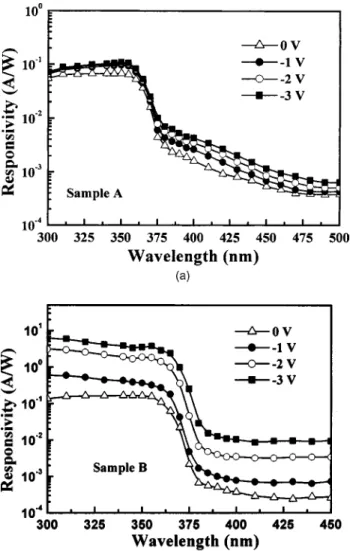
Figures 3共a兲 and 3共b兲 show spectral response of samples A and B, respectively. It was found that cutoff occurred at around 365 nm 共the absorption edge of GaN兲 for both samples. With incident light wavelength of 350 nm and a ⫺1 V reverse bias, it was found that the measured respon-sivity was around 0.1 and 0.37 A/W for samples A and B, respectively. Such a dramatic difference could be attributed to the fact that incident photons (⫽350 nm) are partially absorbed by the LT–GaN cap layer and the photogenerated FIG. 1. Schematic structure of the n⫹-GaN/i-GaN/LT–GaN/Ni/Au
Schottky barrier diode共sample A兲.
FIG. 2. I – V curves taken in dark for samples A and B.
FIG. 3. Spectral responsivity of共a兲 samples A and 共b兲 B measured at dif-ferent reverse biases.
2914 Appl. Phys. Lett., Vol. 82, No. 17, 28 April 2003 Leeet al.
carriers will compensate trap levels in LT GaN. As a result, the photocurrent and responsivity will both become smaller for sample A. It was also found that the responsivity de-creased slowly as the wavelength of the incident light in-creased from 380 to 480 nm for sample A. In contrast, the responsivity of sample B in this wavelength region was near a constant. The below band gap absorption observed from sample A could again be attributed to the defect levels within the band gap of the LT GaN cap layer. Photons in this wave-length region could still excite electrons from deep levels to conduction band, or excite electrons from valence band to deep levels in sample A. Furthermore, it was found that the responsivity of sample A is less bias dependent. In contrast, the much stronger bias dependent responsivity of sample B suggests that there might exist some internal gain in this particular Schottky barrier PD, even at low biases. The exact origin of this internal gain is not clear yet. One possible origin is photoconductive gain induced by the surface defects of sample B. If this is the case, our result seems to imply that LT GaN cap layer could effectively passivate surface defects on the undoped GaN layer. However, this statement is slightly speculative. Further studies need to be performed to clarify this point.
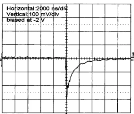
Figure 4 shows a typical transient response when sample A was biased at⫺2 V. It can be seen that the photoresponse of sample A decreased exponentially with an impulse full width at half maximum 共FWHM兲 of around 0.5s. Similar behavior was observed from sample B with a slightly smaller impulse FWHM of 0.4 s. These results suggest that the operation speed of the fabricated PDs is limited by the RC time constant of the devices. Under a ⫺2 V applied bias, it was found that the measured capacitance of samples A and B is around 65 and 83 pF, respectively. The smaller total ca-pacitance of sample A is attributed to the introduction of the LT GaN layer and thus an additional capacitance, CLT, in series with the original device. Although the total capaci-tance of sample A is smaller, its series resiscapaci-tance should be much larger than that of sample B due to the introduction of the highly resistive LT GaN layer. Thus, the operation speed of sample A is slower than that of sample B. In other words, although we could significantly reduce the leakage current
and achieve a much larger photocurrent to dark current con-trast ratio by introducing a LT GaN on top of the conven-tional nitride-based UV PDs, operation speed of the i-GaN/LT GaN/Ni/Au Schottky barrier PDs is also slower than the conventional i-GaN/Ni/Au Schottky barrier PDs.
In summary, i-GaN/LT–GaN/Ni/Au 共sample A兲 and i-GaN/Ni/Au共sample B兲 Schottky barrier UV PDs were pre-pared by OMVPE. It was found that we could significantly reduce the leakage current and achieve a much larger photo-current to dark photo-current contrast ratio by introducing a LT GaN on top of the conventional nitride-based UV PDs. With incident light wavelength of 350 nm and a ⫺1 V reverse bias, it was found that the measured responsivity was around 0.1 and 0.37 A/W for samples A and B, respectively. Further-more, it was found that the operation speed of sample A is slower than that of sample B due to the highly resistive LT– GaN layer induced large RC time constant.
The authors would like to acknowledge the financial support from the National Science Council for their research Grant Nos. NSC 90-2215-E-008-043 and NSC 90-2112-M-008-046. P. W. Yang is also appreciated for performing the device fabrication.
1J. I. Pankove, Mater. Res. Soc. Symp. Proc. 162, 515共1990兲.
2E. Monroy, E. Mun˜oz, F. J. Sa´nchez, F. Calle, E. Calleja, B. Beaumout, P. Gibart, J. A. Mun˜oz, and F. Cusso´, Semicond. Sci. Technol. 13, 1042
共1998兲.
3G. Parish, S. Keller, P. Kozodoy, J. A. Ibbetson, H. Marchand, P. T. Fini, S. B. Fleischer, S. P. DenBaars, and U. K. Mishra, Appl. Phys. Lett. 75, 247共1999兲.
4
E. Monroy, M. Hamilton, D. Walker, P. Kung, F. J. Sa´nchez, and M. Razeghi, Appl. Phys. Lett. 74, 1171共1999兲.
5A. Osinsky, S. Gangopadhyay, R. Gaska, B. Williams, M. A. Khan, D. Kuksenkov, and H. Temkin, Appl. Phys. Lett. 71, 2334共1997兲. 6
Q. Chen, J. W. Yang, A. Osinsky, S. Gangopadhyay, B. Lim, M. Z. Anwar, M. Asif Khan, D. Kuksenkov, and H. Temkin, Appl. Phys. Lett. 70, 2277
共1997兲.
7Z. C. Huang, J. C. Chen, and D. Wickenden, J. Cryst. Growth 170, 362
共1997兲.
8
C. H. Chen, S. J. Chang, Y. K. Su, G. C. Chi, J. Y. Chi, C. A. Chang, J. K. Sheu, and J. F. Chen, IEEE Photonics Technol. Lett. 13, 848共2001兲. 9D. Walker, E. Monroy, P. Kung, J. Wu, M. Hamilton, F. J. Sanchez, J.
Diaz, and M. Razeghi, Appl. Phys. Lett. 74, 762共1999兲. 10
X. A. Cao, S. J. Pearton, G. Dang, A. P. Zhang, F. Ren, and J. M. Van Hove, Appl. Phys. Lett. 75, 4130共1999兲.
11Q. Z. Liu, L. S. Yu, S. S. Lau, J. M. Redwing, N. R. Perkins, and T. F. Kuech, Appl. Phys. Lett. 70, 1275共1997兲.
12L. Wang, M. I. Nathan, T-H. Lim, M. A. Khan, and Q. Chen, Appl. Phys. Lett. 68, 1267共1996兲.
13C. T. Lee, Y. J. Lin, and D. S. Liu, Appl. Phys. Lett. 79, 2573共2001兲. 14J. K. Kim, H. W. Jang, C. M. Jeon, and J.-L. Lee, Appl. Phys. Lett. 81,
4655共2002兲.
15J. K. Sheu, Y. K. Su, G. C. Chi, M. J. Jou, and C. M. Chang, Appl. Phys. Lett. 72, 3317共1998兲.
16S. Lodha, D. B. Janes, and N. P. Chen, Appl. Phys. Lett. 80, 4452共2002兲. 17L. W. Yin, Y. Hwang, J. H. Lee, R. M. Kolabas, R. J. Trew, and U. K.
Mishra, IEEE Electron Device Lett. 11, 561共1990兲. 18
J. K. Sheu, C. J. Kao, M. L. Lee, W. C. Lai, L. S. Yeh, G. C. Chi, S. J. Chang, Y. K. Su, and J. M. Tsai, J. Electron. Mater.共to be published兲. 19J. K. Sheu, Y. K. Su, G. C. Chi, M. J. Jou, C. M. Chang, C. C. Liu, and W.
C. Hung, J. Appl. Phys. 85, 1970共1999兲.
20J. K. Sheu, Y. K. Su, G. C. Chi, M. J. Jou, C. M. Chang, C. C. Liu, W. C. Hung, J. S. Bow, and Y. C. Yu, J. Vac. Sci. Technol. B 18, 729共2000兲. 21M. Lampert and P. Mark, Current Injection in Solids共Academica, New
York, 1970兲. FIG. 4. Typical temporal response of sample A measured at a reverse bias of
⫺2 V.
2915
Appl. Phys. Lett., Vol. 82, No. 17, 28 April 2003 Leeet al.