Chapter 1 Introduction
1.1 Overview
Binnig and Rohrer et al. developed scanning tunneling microscopy (STM) at the IBM Zürich Research Laboratory in 1981. It is used to observe surfaces on the atomic scale. The power of STM has introduced the new age of nanotechnology. The motion of atoms, the structure of surfaces and growth behaviors in real space of several materials are now feasible.
Given the need for stable electric contacts and better performing semiconductor-based devices, understanding epitaxial growth and the reactions of metal with SiGe-based materials are very important. Therefore, metal films on semiconductors should be grown atomically flat, with uniform thickness.
In this work, STM is used to study the deposition of Pb on the Si(111)
surface. The low reactivity and solubility of Pb in the bulk of Si make the
Pb/Si(111) system an appropriate model for studying the metal/semiconductor
system. However, the phase diagram of Pb/Si(111) is very complex, depending
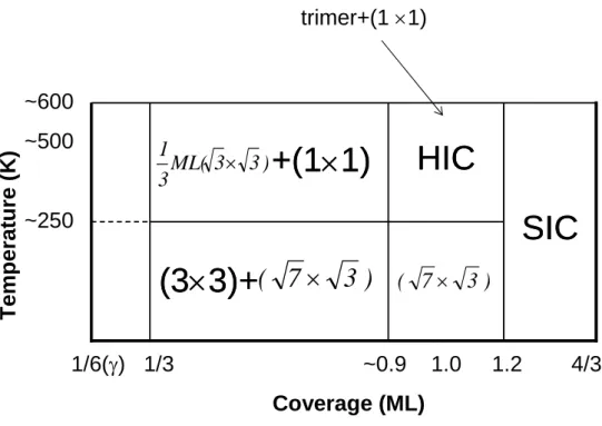
on coverage, temperature and the experimental annealing procedure. For instance, when Pb is deposited on Si(111) with a coverage of 1/6 ML, a so-called mosaic phase (or γ phase) is observed
1,2. When the Pb coverage slightly exceeds 1/3ML, 1/3ML-(
3× 3) phase and (1×1) phase
3are observed. With a coverage between 1 and 4/3ML, a hexagonal incommensurate phase (HIC) and a striped incommensurate phase (SIC) are observed
4,5. The phases of the Pb/Si(111) system vary not only with the Pb coverage, but also with the temperature. For example, when the 1/3ML-(
3× 3) phase and the (1×1) phase are cooled below ~250K, (3×3) and (
7× 3) phases are formed.
However, the SIC phase does not undergo a phase transition, even at 50K. The atomic model proposed by Hwang et al. indicates that the HIC and the SIC phases are composed of three Pb atoms at the T1 sites toward either at the H3 or T4 sites
6,7. Therefore, based on the trimers model of Hwang et al., the Pb coverages of HIC and SIC phases are 1ML rather than between 1 and 4/3 ML.
Hupalo et al. recently proposed the “devil’s staircase phase diagram” of the Pb/Si(111) system with a Pb coverage of between 1 and 4/3ML. The phase diagram is derived using the 1-D Ising theoretical model, and established theoretically for the Pb/Si(111) system. However, the presence of defects in any experiment is inevitable. Accordingly, the effect of defects on the phase transition is observed in situ and discussed in the first part of this investigation.
The staircase phase diagram is also obtained from experimental results.
The presence of corner holes makes the Si(111)-(7×7) surface imperfect.
Earlier studies
8indicate that a quantum-well state may not be present on the site of the corner hole of the Si(111)-(7×7) surface. The effect of this fact on the nucleation properties and the growth behaviors of Pb deposited on the Si(111) surface are experimentally examined.
In the incommensurate phase (IC) of the Pb/ Si(111) system, unlike on the Si(111)7×7 surface, quantum-well states are observed everywhere
9. The homogeneity of electronic properties can be exploited to grow atomically flat Pb films. The growth behavior of Pb deposited on the IC phase at low temperature (55K, 100K and 140K) is studied. The third part of this thesis presents experimental observations.
When Pb is deposited on the IC phase at ~200K, Pb grows in
preference to Pb islands. In the incommensurate phase of the Pb/ Si(111)
system, quantum Pb islands have been grown, and found two yield
distinguishable image contrast patterns
10. Contrast patterns vary with the
applied bias and the thickness of the Pb islands, originating mainly from the
electronic effect. Type I Pb islands, with a strong image contrast, act as
templates for the nucleation of nanoclusters (or nanopucks). The fourth section
of this work presents the results. Ag nanopucks are grown in highly ordered
two-dimensional arrays on Type I Pb islands in a pronounced wide plateau
region between ~70K and ~150K. The substrate strongly affects the growth
behavior. Scaling theory does not elucidate the growth behavior. Thus, the trapping strength of the substrate is quantified. The quantitative results reveal that the trapping powers of Type I and Type II for Ag nanopucks differ markedly.
This investigation considers the growth behavior of Ag to elucidate the bi-layer oscillatory characteristic of Pb islands. Furthermore, dI/dV measurements of Ag nanopucks nucleated at different sites exhibit the same characteristic.
dI/dV measurements indicate that x-, y-confinement must be involved in
determining the electronic properties of Ag nanopucks. Therefore, the last section on experimental results addresses the electronic structures of Ag nanopucks. The site-dependent characteristics of the electronic structures and the size-, shape-dependent properties are examined. The effect of the substrate on the electronic structures of the Ag adsorbates is also investigated.
1.2 Principles of scanning tunneling microscopy (STM) 11
The most important physical effect in STM is the electronic tunneling
effect. In quantum mechanics, within a classically forbidden region, the
wavefunction ϕ ( ) z has the solution ( ) ( )
η ) ( , 2
0 m U E
e
z
z−
=
= ϕ
−κ
ϕ
κwhich
satisfies Schrödinger’s equation,
( ) ( ) ( ) z U z z E ( ) z dz
d
m ϕ + ϕ = ϕ
−
2 222
η .
Therefore, the probability density, p ∝ ϕ
n( ) 0
2e
−2κz, must be non-zero to enable the barrier to be penetrated. When a bias voltage V is applied, the tunneling probability density near the Fermi level is proportional to the tunneling current
∑ ( )
−
∝
F −F
E
eV E
z
n
e
I ϕ 0
2 2κ.
1.3 STM operating modes 11-13
STM is typically used in two modes. Involve different control
parameters. These two modes are respectively interaction between the tip and
the sample, and the control of the tip with a fixed z position. When the
interaction between the tip and the sample is constant, the STM is in “the
constant current mode”. When the z position is fixed, it is in “the constant
height mode”.
(a) Constant current mode
In this mode, during scanning, the interaction between tip and sample is set with a fixed current I
0and bias voltage V
0to cause a constant tunneling current to flow between these two electrodes. Therefore, the z-position of the tip responds to the interaction intensity between the tip and the sample from the sample : the separation of the tip from the sample is constantly adjusted via a feedback loop system, which forces the piezoelectric driver of the tip.
Accordingly, a topographical image can be obtained by recording the height of the tip as a function of position.
The constant current mode is properly applied when the investigated surfaces are not flat on the atomic scale. The surface features can be elucidated according to the sensitivity of the piezoelectric driver. However, the disadvantage of this mode is the limited scan speed governed by the finite response time of the feedback loop.
(b) Constant height mode
The constant height mode is utilized to increase the scan speed
significantly. In constant height mode, the time constant of the feedback system
is made long or eliminated. The tip can be rapidly scanned at constant height
over the surface of the sample. Thus, the variations in the tunneling current are
recorded as a function of position to yield a topographic image. However,
although turning off the feedback loop system provides the great advantage of
faster scanning, it also makes the constant height mode effective only for relatively flat samples.
(c) Current image tunneling spectroscopy (CITS)
STM yields not only the topographic image but also information on local electronic spectroscopic properties. Electronic spectroscopy elucidates the local density of electronic states of interest and is very important in surface science and nanoscience. Current image tunneling spectroscopy (CITS)
14is particularly elegant. The polarity of the applied bias voltage, V, between the sample and the tip determines whether the tunneling current flows into the unoccupied states of the sample (positive sample bias) or out of the occupied states (negative sample bias). The tunneling current I comprises all of the tunneling probability associated with the sample states in the interval eV, and can be represented as
( )
zE
eV E
n
e
I
F
F
ϕ 0
2 −2κ∑
−∝ .
The local density of states (LDOS) ρ
S( Z , E ) is defined as
( )
2) 1 ,
( ∑
−
≡
EE n
S
z E z
ε
ε ϕ
ρ .
for a small value ε . Therefore, the relationship between the tunneling current
and the LDOS can be written as,
e
zE o V
I ∝ ρ ( ,
F)
−2κ. The sample wavefunction is
( ) ( ) z ϕ e
κzϕ = 0
−,
so ∑ ( ) ∑ ( ) ( )
− −
−
= =
∝
FF
F
F
E
eV E
E
eV E
F s z
n