Studies of InGaN/ GaN multiquantum-well green-light-emitting diodes grown by metalorganic chemical vapor deposition
K. S. Ramaiah,
a)Y. K. Su, S. J. Chang, C. H. Chen, and F. S. Juang
Department of Electrical Engineering, National Cheng Kung University, Tainan 701, Taiwan, Republic of China
H. P. Liu and I. G. Chen
Department of Materials Science and Engineering, National Cheng Kung University Tainan 701, Taiwan, Republic of China
(Received 9 January 2004; accepted 26 May 2004)
InGaN 共3 nm兲/GaN共5 nm兲 three period multiquantum green-light-emitting diodes (LEDs) grown by the metalorganic chemical vapor deposition technique have been studied using high-resolution transmission electron microscopy (HRTEM), double crystal high resolution x-ray diffraction (HRXRD) and low temperature photoluminescence. HRTEM analysis showed that the defect density gradually decreased in the growth direction with increasing thickness. Self-assembled quantum dot-like structures in the wells and black lumps between the well and barrier due to In segregation and strain contrast were observed, respectively. The HRXRD spectrum of the green LED structure was simulated using the kinematical theory method to obtain the composition and thickness of the well and barrier. The quantum-well (QW) green emission peak 2.557 eV at 10 K showed “S” shaped shift like a red–blue–red shift with variation of the temperature in the photoluminescence spectra due to potential fluctuations caused by inhomogeneous alloy distribution in the wells. The activation energy of 49 meV obtained from the QW green emission line indicated deepening of the localization of the carriers. © 2004 American Institute of Physics.
[DOI: 10.1063/1.1773371]
Group III nitrides play a major role in optoelectronic devices despite their high density of defect levels 共10
9cm
−2兲.
High brightness light-emitting diodes (LEDs) are now com- mercially available, however green LEDs show less effi- ciency than that of blue LEDs,
1therefore investigations of green LED structures are essential in order to understand their device physics. Deposition parameters such as well, barrier widths and carrier sheet density are important criteria in optoelectronic devices,
2in the case of laser diodes, to obtain a quasifield-free shaped quantum well, where the fa- vorable sheet density is 5 ⫻10
12cm
−2and for lasing action the well width should be less than 5 nm.
3Group III nitrides generate large piezoelectric fields because of their large pi- ezoelectric constants, which lead to the quantum confined Stark effect on the optical properties. The InGaN layers are active regions in the device in which In segregation or phase separation is the main drawback. The segregation of In is due to large lattice mismatch and low miscibility between GaN and InN compounds, which cause large compositional fluc- tuations in the InGaN layers.
4In this letter, we report the structural and optical properties of green-light-emitting di- odes.
The green-light-emitting devices studied in this work were grown by metalorganic chemical vapor deposition (MOCVD). A GaN buffer layer with thickness of 25 nm was first grown on c-plane sapphire substrates at low temperature of 560° C, followed by a 2 m thick Si doped GaN layer at higher temperature of 1060° C, on which a three period 3 nm InGaN well/ 5 nm GaN barrier was then grown at low tem-
perature of 780° C using N
2only as the carrier gas, followed by a 0.1 m p-AlGaN cladding layer and finally p-GaN with thickness of 0.5 m was deposited. Metalor- ganic sources such as trimethylgallium, trimethylindium, trimethylaluminum, and NH
3were used as precursors for Ga, In, Al, and radical nitrogen, respectively.
In order to study the microstructure of the layers, the back surface of the samples was mechanically polished and then thinned by an Ar
+ion milling. A Philips transmission electron microscope was operated at 200 kV to obtain struc- tural data. The samples were characterized using a Philips X-Pert double crystal x-ray diffractometer (XRD) with a Ge 共220兲 single crystal, operated at 40 kV and 50 mA with radiation of 1.540 56 Å. A He– Cd laser used at 325 nm for excitation, a GaAs based photodetector used to record ex- cited emission, and a closed loop He cryostat for low tem- perature were employed.
The density of defect levels gradually decreased in the growth direction from 10
9to 10
8cm
−2and some of the nanopipe-like structures existed in the Si-doped GaN layer, and after growth of quantum wells on it the density of de- fects drastically reduced and propagation of some of the de- fect levels ended up underneath the quantum wells, as shown in Fig. 1 (a). This could be due to partial reduction of strain in the layers. A transmission electron microscopy (TEM) mi- crograph showed a quantum dot-like structures in the wells due to segregation of In [Fig. 1(b)]. The dark regions of contrast formed between the well and barrier due to strain and In precipitation was high indicating In phase immiscibil- ity with GaN, which continued into the cap layer of GaN deposited on the InGaN/ GaN quantum wells.
5The segrega- tion of In was high with increasing In concentration in the quantum wells. In order to shift emission wavelength from
a)Corresponding author; present address: Department of Electrical Engineer- ing, Virginia Commonwealth University, 601 W. Main St., Richmond, VA 23284; electronic mail: [email protected]
APPLIED PHYSICS LETTERS VOLUME 85, NUMBER 3 19 JULY 2004
0003-6951/2004/85(3)/401/3/$20.00 401 © 2004 American Institute of Physics
Downloaded 09 Oct 2009 to 140.116.208.53. Redistribution subject to AIP license or copyright; see http://apl.aip.org/apl/copyright.jsp
blue to yellow, In percentage has to be increased, as shown explicitly from our results.
6The well and barrier period width was found to be ⬃9 nm.
XRD analysis revealed that the In composition and pe- riod were found to be 13.5% and 8.6 nm from simulation of a / 2 scan of the (0004) curve, as shown in Fig. 2; the In composition obtained from XRD is quite low compared to that in photoluminescence (PL) analysis (In of 24%). The reason why is that the PL emission is basically from the active layers of quantum wells, which contained not only the quantum dot-like structures, which provided efficient radia- tive recombination centers rather than ordinary layers, the In-rich GaN matrix favors longer wavelength emission but also the quantum confined Stark effect whereas XRD analy- sis showed an average approximate In composition in the well layers.
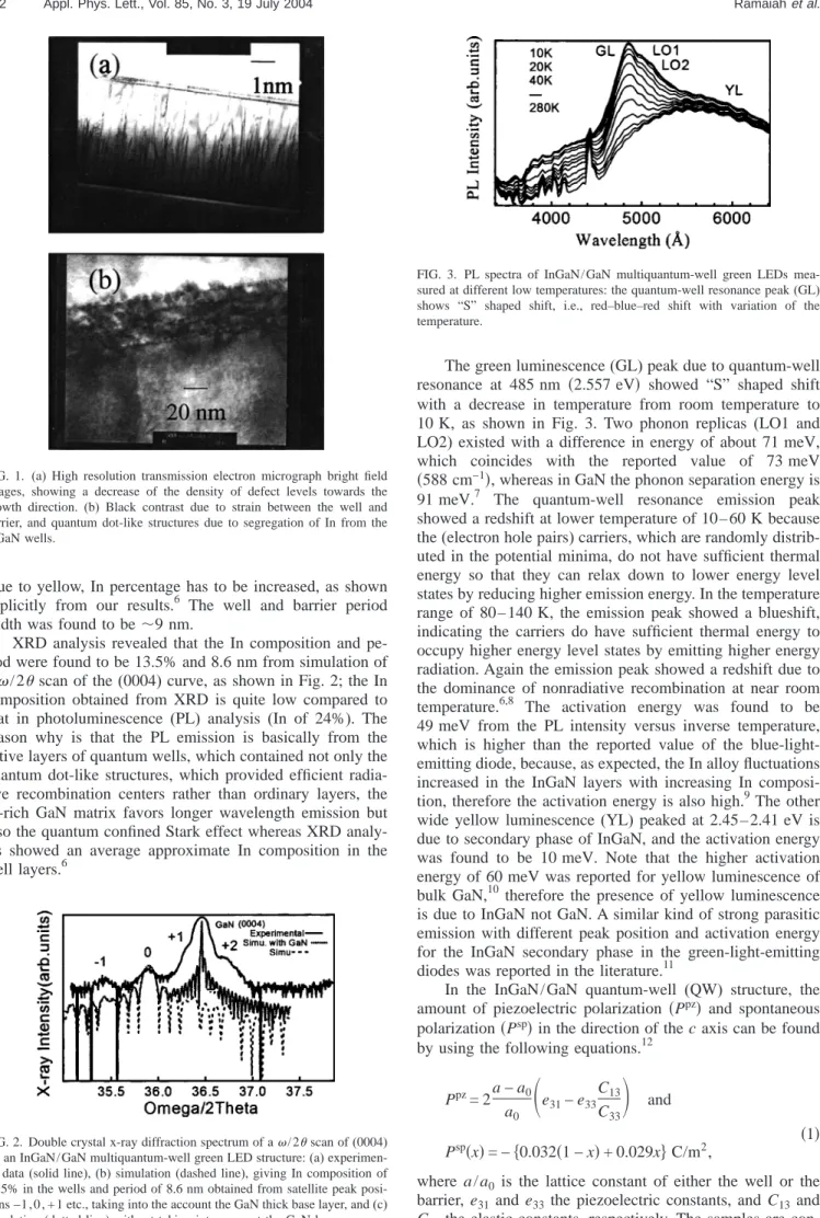
6The green luminescence (GL) peak due to quantum-well resonance at 485 nm 共2.557 eV兲 showed “S” shaped shift with a decrease in temperature from room temperature to 10 K, as shown in Fig. 3. Two phonon replicas (LO1 and LO2) existed with a difference in energy of about 71 meV, which coincides with the reported value of 73 meV 共588 cm
−1兲, whereas in GaN the phonon separation energy is 91 meV.
7The quantum-well resonance emission peak showed a redshift at lower temperature of 10– 60 K because the (electron hole pairs) carriers, which are randomly distrib- uted in the potential minima, do not have sufficient thermal energy so that they can relax down to lower energy level states by reducing higher emission energy. In the temperature range of 80– 140 K, the emission peak showed a blueshift, indicating the carriers do have sufficient thermal energy to occupy higher energy level states by emitting higher energy radiation. Again the emission peak showed a redshift due to the dominance of nonradiative recombination at near room temperature.
6,8The activation energy was found to be 49 meV from the PL intensity versus inverse temperature, which is higher than the reported value of the blue-light- emitting diode, because, as expected, the In alloy fluctuations increased in the InGaN layers with increasing In composi- tion, therefore the activation energy is also high.
9The other wide yellow luminescence (YL) peaked at 2.45–2.41 eV is due to secondary phase of InGaN, and the activation energy was found to be 10 meV. Note that the higher activation energy of 60 meV was reported for yellow luminescence of bulk GaN,
10therefore the presence of yellow luminescence is due to InGaN not GaN. A similar kind of strong parasitic emission with different peak position and activation energy for the InGaN secondary phase in the green-light-emitting diodes was reported in the literature.
11In the InGaN/ GaN quantum-well (QW) structure, the amount of piezoelectric polarization 共P
pz兲 and spontaneous polarization 共P
sp兲 in the direction of the c axis can be found by using the following equations.
12P
pz= 2 a − a
0a
0冉 e
31− e
33C C
1333冊 and
共1兲 P
sp共x兲 = − 兵0.032共1 − x兲 + 0.029x其 C/m
2,
where a / a
0is the lattice constant of either the well or the barrier, e
31and e
33the piezoelectric constants, and C
13and C
33the elastic constants, respectively. The samples are con-
FIG. 1. (a) High resolution transmission electron micrograph bright field images, showing a decrease of the density of defect levels towards the growth direction. (b) Black contrast due to strain between the well and barrier, and quantum dot-like structures due to segregation of In from the InGaN wells.
FIG. 2. Double crystal x-ray diffraction spectrum of a/ 2scan of(0004) for an InGaN/ GaN multiquantum-well green LED structure:(a) experimen- tal data(solid line), (b) simulation (dashed line), giving In composition of 13.5% in the wells and period of 8.6 nm obtained from satellite peak posi- tions −1 , 0 , + 1 etc., taking into the account the GaN thick base layer, and(c) simulation(dotted line) without taking into account the GaN layer.
FIG. 3. PL spectra of InGaN/ GaN multiquantum-well green LEDs mea- sured at different low temperatures: the quantum-well resonance peak(GL) shows “S” shaped shift, i.e., red–blue–red shift with variation of the temperature.
402 Appl. Phys. Lett., Vol. 85, No. 3, 19 July 2004 Ramaiahet al.
Downloaded 09 Oct 2009 to 140.116.208.53. Redistribution subject to AIP license or copyright; see http://apl.aip.org/apl/copyright.jsp
sidered Ga-face layers. The electric field in the well and barrier can be determined by using the expressions,
F
W= L
B
BL
W+
WL
B关兩P
B pz兩 + 兩P
Bsp
兩 − 兩P
W sp兩 − 兩P
Wpz
兩兴, 共2兲
F
B= L
W
BL
W+
WL
B关兩P
W sp兩 + 兩P
Wpz
兩 − 兩P
B pz兩 − 兩P
Bsp
兩兴, 共3兲
where is the dielectric constant, L is the width, and B共W兲 represents the barrier (well).
The QW ground level transition energy can be estimated as
E
1e1h= E
g− eF
WL
W+ 冉 9 8 បeF
冑2
W冊
2/3冉 m 1
e+ m 1
h冊
1/3, 共4兲
where E
gis the band gap of the quantum well, m
ethe elec- tron effective mass, and m
hthe hole effective mass. In Eq.
(4), the second term represents the redshift due to the electric field in the well and the third term is for the blueshift due to electron and hole confined states. The quantum-well ground level emission 共E
1e1h兲 value was found to be 2.557 eV, E
gvalue of 2.523 eV and electrostatic field strength of 1.0
⫻10
5V / cm for the In
0.24Ga
0.76N / GaN quantum well, con- sidering InN E
g= 0.77 eV. The QW ground level emission shift of 34 meV 共2.557–2.523 eV兲 was due to the domi- nance of the quantum confined Stark effect.
13In summary, the decrease of defect density propagation towards the growth direction, quantum dot-like structures due to In phase separation in green LEDs, were observed and the well and barrier widths obtained from TEM analysis co- incided with those of the XRD results. The low temperature PL studies showed “S” shaped shift, i.e., red–blue–red shift for quantum-well emission and it is attributed to potential
fluctuations caused by the InGaN alloy inhomogeneity. The higher activation energy of 49 meV for green LEDs is an indication of the deep localization energies of excitons.
The authors would like to thank the National Science Council (NSC), Taipei for partial financial support under Contract No. NSC 85-2215-E-006-004. The authors thank Professor H. Morkoç and Professor D. Johnstone for fruitful discussions.
1S. Nakamura and S. F. Chichibu, Introduction to Nitride Semiconductor Blue Lasers and Light Emitting Diodes (Taylor and Francis, London, 2000).
2Q. Zhou, J. Chen, B. Pattada, M. O. Manasreh, F. Xiu, S. Puntigan, L. He, K. S. Ramaiah, and H. Morkoç, J. Appl. Phys. 93, 10140(2003).
3F. D. Sala, A. D. Carlo, P. Lugli, F. Bernardini, V. Fiorentini, R. Scholz, and J. Jancu, Appl. Phys. Lett. 74, 2002(1999).
4M. J. Reed, N. A. El-Masry, C. A. Parker, J. C. Roberts, and S. M. Bedair, Appl. Phys. Lett. 77, 4121(2000).
5M. D. McCluskey, L. T. Romano, B. S. Krusor, D. P. Bour, and S. Bren- nan, Appl. Phys. Lett. 72, 1730(1998).
6K. S. Ramaiah, D. Huang, M. A. Reshchikov, F. Yun, H. Morkoc, J.
Jasanski, Z. Liliental-Weber, S. C. Sone, and S. H. Park, J. Mater. Sci.:
Mater. Electron. 11, 239(2003).
7T. Inushima, V. V. Mamutin, V. A. Vekshin, S. V. Ivanov, T. Sakon, M.
Motokawa, and S. Ohoya, J. Cryst. Growth 227–228, 481(2001).
8Y. Han, H. Chen, H. B. Yu, D. S. Li, Z. B. Yan, Q. Huang, and J. M. Zhou, J. Cryst. Growth 253, 203(2003).
9H. P. D. Schenk, M. Leroux, and P. de Mierry, J. Appl. Phys. 88, 1525 (2000).
10A. P. Young and L. J. Brillson, Appl. Phys. Lett. 77, 699(2000).
11Y. Sun, Y. H. Cho, E. K. Suh, H. J. Lee, R. J. Choi, and Y. B. Hahn, Appl.
Phys. Lett. 84, 49(2004).
12O. Ambacher, J. Smart, J. R. Shealy, N. G. Weimann, K. Chu, M. Murphy, W. J. Schaff, L. F. Eastman, R. Dimitrov, L. Wittmer, M. Stutzmann, W.
Rieger, and J. Hilsenbeck, J. Appl. Phys. 85, 3222(1999).
13J. Dalfors, J. P. Bergman, P. O. Holtz, B. E. Sernelius, B. Monemar, H.
Amano, and I. Akasaki, Appl. Phys. Lett. 74, 3299(1999).
Appl. Phys. Lett., Vol. 85, No. 3, 19 July 2004 Ramaiahet al. 403
Downloaded 09 Oct 2009 to 140.116.208.53. Redistribution subject to AIP license or copyright; see http://apl.aip.org/apl/copyright.jsp