Analysis of a Coupled Inductor for Zero-Current Transition Boost Converters
Masanori Kobayashi and Nobuyuki Kasa Dept. of Electrical and Electronic Engineering
Okayama University of Science Okayama, Japan kasa@ee.ous.ac.jp
Abstract—This paper presents an analysis of a coupled inductor for zero-current transition (ZCT) converters. In order to reduce switching losses and noises, a soft-switching technique is adopted.
It is suitable for the pulse-width modulation (PWM), because the resonant transition is very short and it is independent of the switching frequency. We adapt a coupled inductor which consists of a boost inductor and a resonant inductor to ZCT converters.
To analyze and simulate a magnetic field distribution of the coupled inductor, the ANSYS software is employed. A prototype converter is implemented by a field programmable gate array (FPGA) and a 2.5MHz analog to digital (A/D) converter. From the experimental results, the zero-current transition operation of the main switch is confirmed and the efficiency of the converter using the coupled inductor is improved.
Keywords-boost converter; soft-switching; coupled inductor;
ZCS
I. I
NTRODUCTIONIn renewable generation systems, boost converters are used for low input voltage of batteries to supply the energy to the loads. Therefore, efficiency and response of the converter are required to be high level.
In a conventional converter, insulated gate bipolar transistors (IGBT) are used as the semiconductor main switches. However, the power losses, caused by the IGBT tail currents and their resister-capacitor-diode (RCD) snubber circuits, make the system efficiency low. In order to improve the efficiency, soft switching techniques are adapted[1-4].
This paper presents an analysis of a coupled inductor for zero-current transition (ZCT) converters. In order to reduce switching losses and noises, a soft-switching technique is adopted. It is suitable for the pulse-width modulation (PWM), because the resonant transition is very short and it is independent of the switching frequency. However, the resonant current adds the inductor current and the phenomenon affects the efficiency. To improve the efficiency, a coupled inductor is adopted to the system. The winding for the boost inductor and the winding for the resonant inductor are wound around the same core. To analyze and simulate a magnetic field distribution in the core of the coupled inductor, the
ANSYS software is employed. From the simulation results, the flux density of the core is affected by the direction of the current.
In a prototype system, a field programmable gate array (FPGA) and a 2.5MHz analog to digital (A/D) converter can control the inductor current of the ZCT converter. Since the ratio of the output voltage to input voltage is more than 2 times, the duty ratio is more than 50 %. The inductor current is controlled precisely even if the inductor current is operated in the continuous conduction mode (CCM.)
From the experimental results, the zero-current transition operation of the main switch is confirmed and the efficiency of the converter using the coupled inductor is improved.
II. C
OUPLEDI
NDUCTOR FORZCT C
ONVERTERA. Construction of Coupled Inductor
coupled inductor
Vin
Sa1 Cr
Sm1
Lr
Ca
L
Da1 Da2 Dm1
Dm2
Da3
Vo
C
ZCT circuit
Fig. 1 Proposed ZCT boost converter
The efficiency of converters is greatly influenced by the losses caused by the hard switching of a main switch and the RCD snubber across it. Therefore, to solve these problems, we propose a ZCT circuit for the converter.
Fig. 1 shows the main circuit configuration for a prototyped ZCT converter. The ZCT circuit consists of a resonant capacitor C
rand inductor L
r, an auxiliary switch Sa1, three
to the main switch in parallel, and then it is useful for any topologies. A main switch Sm1 can be turned off under the zero current condition after the auxiliary switch Sa1 is turned on.
Fig. 2 shows the key voltage and current waveforms of the converter. T
SWis the one switching duration. There are seven intervals of operation for the converter
To improve the efficiency, a coupled inductor is adopted to the system. Fig. 3 (a) shows the conventional inductors which are the main inductor L and the resonance inductor L
r. As the coupled inductor is shown in fig. 3 (b), the main inductor and the resonance inductor are integrated on the same core. The primary winding of the coupled inductor is used as the boost inductor L. The secondary winding of it is used as the resonant inductor L
r.
In the interval 6 (t5<t<t6), the both of the currents of
t0 t1 t2 t3 t4 t5 t6 Tsw+t0
Sm1
Sa1
iCa
ism1+iDm1
iLr
vCr
-vCrmax
vCrmax
t’1
t0 t1 t2 t3 t4 t5 t6 Tsw+t0
Sm1
Sa1
iCa
ism1+iDm1
iLr
vCr
-vCrmax
vCrmax
t’1
Fig. 2 Typical waveforms in one switching duration or Tsw to illustrate the principle of operation of ZCT converter.
L L
r(a) non coupled
L
rL
(b) coupled inductor
Fig. 3 Inductors for boost and resonance.
32mm
50mm 25.5mm
20mm
1mm
9.5mm
Fig. 4 CAD model of inductor.
coupled inductor flow through the windings. When Sm1 is turned on at t5, both the source current i
inand the resonant current i
Lrthrough L
rand C
rbegins to flow into Sm1. When the resonant current i
Lrreaches the crest value in negative direction, the Sm1 current iSm1 becomes the maximum value.
After a half of resonant cycle, i
Lrdecreases to zero, i
Sm1becomes to the same level as i
inat t6.
B. Simulation Results of the Copuled Inductor
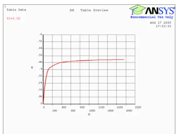
To analyze and simulate a magnetic field distribution, the ANSYS software is employed. Fig. 4 shows a CAD model and Fig. 5 shows the B-H curve of the core. The core is made by ferrite (TDK:PC44PQ50/50Z-13.)
We analyze the flux density in the core during the interval 6.
The magnetomotive force in the boost inductor is 80 AT. The magnetomotive force in the resonant inductor is 24.5 AT or 19.5 AT, which is selected in the direction of the current.
Fig. 6 shows the simulation results of the coupled inductor.
The arrows indicate the direction of the flux vectors and the flux densities are colored. Fig. 6 (a) shows the flux by the main
inductor and the one by the resonance inductor flow in the core in the same direction. On the other hand, Fig. 6 (b) shows the flux by the main inductor and the one by the resonance inductor flow in the core in the opposite direction. From the simulation results, the area of high flux density in (a) is wider than the one in (b). It means that the fluxes which flow in the same direction in the core saturate easily.
Therefore, it is expected that the efficiency may be improved by using the coupled inductor whose currents flows in the opposite direction.
III. D
IGITALC
URRENTC
ONTROLLERWhen the inductor current is controlled in the CCM, an external ramp is added to the current controller to stabilize the current feedback loop. In the proposed system, a digital
Fig. 7 Proposed digital current controller in FPGA
20.5us
…
…
…
…
…
…
…
…
…
…
…
…
…
…
…
…
…
…
input
comparator
CLK (25MHz)
parallel output
down counter
Sa1
Sm1 AD(2.5MHz)
counter t
t
t
t
t
t t t t C8_B (48kHz)
parallel data 12 bit
parallel data 12 bit
comparator output
ST
… …
0.48us
Fig. 8 Timing chart of digital current controller in FPGA (b) same direction
(b) opposite direction Fig. 6 Simulation results by ANSYS.
STSW/2
0.64μs 20.48μs
controller is adopted to control the inductor current in the CCM. The digital current controller is implemented on FPGA.
A. Block Diagram and Timing Chart of Controller
Fig. 7 shows the block diagram of the current controller and Fig. 8 shows the timing chart. The frequency of the main clock CLK is 25 MHz. The switching frequency of the converter is obtained by counting the CLK to 511 (=2
9-1) and then the frequency becomes 48.8 kHz. The inductor current AD_DATA is measured as a voltage across a shunt resistor through a 2.5MHz A/D converter. A commanded value of the peak inductor current CMD_DATA is calculated in DSP and the commanded current is send as 12 bit data from DSP to FPGA through a parallel port. To achieve the external ramp in FPGA, a down counter is added to the controller. The down counter counts from the commanded current CMD during one switching term. A comparator compares the output from the down counter CM to the inductor current AD. When AD is more than the output CM, the comparator outputs 1. In the conventional converter, the switch is turned off when the output of the comparator is changed. However, in the proposed ZCT converter, the aux switch must be turned on before the main switch is turned off as explained in section II. A Johnson counter and a SR flip flop are used for the switches to achieve the ZCT.
B. Transfer Function of Converter
The transfer function of the converter is expressed as follows[5],[8]:
LC D T L S V LC
I D T RC z T V LS z V z
G SW
in L SW SW
in
C 1 ' 2 '2
1 )
( +
⎟⎠
⎜ ⎞
⎝⎛ + +
⎟⎠
⎜ ⎞
⎝
⎛ − +
⎭⎬
⎫
⎩⎨
⎧
⎟⎟⎠
⎜⎜ ⎞
⎝
⎛
− +
−
=
(1) Where, S is the down count during the switching period, D’
is the off duty ratio of the main switch and R is the load.
Since the second term of the left hand in (1) is small value, the stability is satisfied by
1 1
)
( ⎟⎟⎠ <
⎜⎜ ⎞
⎝
⎛
− +
−
=
in C
V LS S V
f
(2)
In the prototype system, the count is calculated by the resolution of the A/D converter (10 A /11 bit) as
2048 10 384×
= TSW
S
(3)
Then, the function of stability is calculated as
85. 0 ) (S =
f
(4)
and the system is stable.
IV. E
XPERIMENTALR
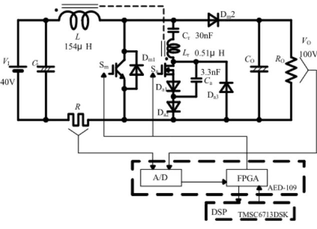
ESULTSBased on the foregoing design method, an experimental system was assembled in the laboratory as shown in Fig. 9. The
converter consists of the main switch Sm1 (IGBT:
IRG4PC40UD, 600V, 20A) and the auxiliary switch Sa1 (MOSFET: IRFPS37N50A, 500V, 36A). The system controller consists of a mother board (DSK6713 made by TI: DSP
VI CB
L
R Sm
Dm1
Da1
Da2
Ca
Lr
Cr
Da3
CO
VO
A/D FPGA
DSP Sa
AED-109 TMSC6713DSK 40V
154μ H 100V
0.51μ H 30nF
3.3nF
RO
Dm2
CI
Fig. 9 Prototype system implemented on DSP and FPGA
Collector current Collector Emitter voltage
50V
5A
(a) voltage and current waveforms of main switch
Drain current
Drain Source voltage 50V
5A
(b) voltage and current waveforms of auxiliary switch Fig. 10 Waveforms of switches
TMS670C6713) and a daughter board (AED-109 made by Signalware: FPGA VertexE200 made by Xilinx).
The input voltage is 40V and the commanded output voltage is set as 100 V. Fig. 10 shows the waveforms of the switch voltages and currents, in using the coupled inductor.
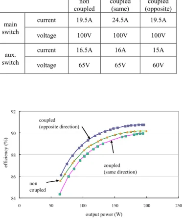
Table 1 shows peak values of currents and voltages of the switches, when the conventional inductors are replaced with the coupled inductor in the ZCT converter. When the currents through the coupled inductor flow in the opposite direction, the peak values of the voltages and the currents of the switches are the smallest values. Under the condition where the output
power is approximately 200W, the efficiency of the converter using the coupled inductor in the opposite direction is approximately 91% and it is approximately 1 point higher than the conventional non coupled converter as shown in Fig. 11.
V. C
ONCLUSIONSThe coupled inductor for ZCT converters has been analyzed. To achieve ZCS of the main switch, ZCT circuits have been adapted to the converter. From the experimental results, we confirmed ZCS turn-off of the main switch. It is confirmed that the efficiency of the converter can be increased by the soft-switching technology using the coupled inductor.
In addition, a digital controller for the inductor current of the converter has been proposed. To avoid distortion in CCM, a down counter is used in FPGA. From the experimental results, the response of the converter can be increased by the current controller.
Therefore, the proposed converter is suitable for the converter in renewable generation systems.
R
EFERENCES[1] G.Hua, E.X.Yang, Y.Jiang and F.C.Lee, “Novel zero-current-transition PWM converters”, IEEE PESC, p.538 (1993)
[2] O. Dranga, B. Buti and I. Nagy, “Stability Analysis of a Feedback- Controlled Resonant DC-DC Converter,” IEEE Trans. on Industrial Electronics, vol. 50, no. 1, pp.141-152, February 2003
[3] P. Chen and A.K.S. Bhat, “A Soft-Switched AC to DC Converter Operating in DCM: Analysis, Design, Simulation and Experimental Results,” IEEE APEC (2004)
[4] R. Ridley, “A New, Continuous-Time Model For Current-Mode Control, IEEE Trans. on Power Electronics, vol. 6, no. 2, April, pp.271-280, 1991 [5] J.G. Kassakian, M.F. Schlecht, and G.C. Verghese, Principles of Power
Electronic, Addison-Wesley, Massachusetts, 1991
[6] N. Kasa, Y. Harada, T. Iida and A. Bhat, “Zero-current transition converters for independent small scale power network system using lower power wind turbines,” International Symposium on Power Electronics, Electrical Drives, Automation and Motion (SPEEDAM), 2006
[7] N. Kasa and T. Iida, “A Digital Current Controller for Zero-Current Transition Bidirectional Converter,” 13th Power Electronics and Motion Control Conference, 2008
[8] N. Kasa, M. Kobayashi and T. Iida, “Digital Current Control Method for Zero-Current Transition Converters,” Journal of the Japan Institue of Power Electronics, vol. 34, pp. 120-126, 2009
Table 1
Peak values of currents and voltages of the switches
non coupled
coupled (same)
coupled (opposite) main
switch
current 19.5A 24.5A 19.5A voltage 100V 100V 100V
aux.
switch
current 16.5A 16A 15A voltage 65V 65V 60V
84 86 88 90 92
0 50 100 150 200 250
output power (W)
efficiency (%)
coupled (opposite direction)
coupled (same direction) non
coupled
Fig. 11 Efficiencies of converters