Constant Frequency Hysteretic PWM Controlled Buck Converter
Kiichiro TANIGUCHI,
Terukazu SATO, Takashi NABESHIMA, and Kimihiro NISHIJIMA
Faculty of Engineering Oita University 700, Dannoharu, Oita, 870-1192 Japan
E-mail: v08e2020@mail.cc.oita-u.ac.jp Abstract -- This paper presents a constant frequency
hysteretic PWM controlled buck converter. In order to have good transient responses for input voltage and load current changes, a new PWM control method with inherent derivative characteristics is proposed. The proposed PWM controller consists of a comparator, a simple RC network and operational amplifier, and it can be synchronized with an external clock signal. Since the converter operates at a constant frequency, it is easy not only to design an output filter but also to apply to multi-phase converters. The theoretical and experimental verification of the proposed method are presented and excellent steady state, dynamic performances, and transient characteristics are realized.
Index Terms-- constant frequency; hysteretic PWM controller; hysteretic comparator; buck converter;
synchronization; hysteretic window; frequency characteristics;
transient responses; load regulation I. INTRODUCTION
With the development of integrated circuit technology, switching power supplies have been widely used in many applications because of smaller size, lighter weight and higher efficiency. Among various kinds of electronic equipment, the power supplies for digital IC’s, such as microprocessors, must have a good dynamic performance for input voltage and the large load current change with high slew rate [1]-[3]. For the digital IC’s that have a current rating of under 15A, a hysteretic PWM controlled buck converter is widely used such as a POL converter since it has the advantage of fast transient response for large load transient [4],[5] and the capability of higher switching frequency. However, for higher current rating than 15A, it is necessary to employ multi-phase converter, and it is necessary to adopt a new control method synchronized with a clock signal.
This paper presents a constant frequency hysteretic PWM controlled buck converter synchronized with a clock signal by using simple method. The operation of the control circuit is described and the steady state and dynamic characteristics of the proposed converter are analyzed. The steady state and dynamic characteristics and frequency characteristics are examined and confirmed by experiments.
II. CONTROL CIRCUIT AND OPERATION A. Conventional Circuit And Operation
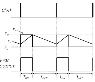
Fig.1 shows the buck converter with the conventional hysteretic PWM controller [5] and Fig.2 shows operating waveforms of hysteretic comparator. The control circuit consists of a comparator with hysteresis. The operating waveforms of the comparator are shown in Fig.2. Upper and lower threshold voltage VH and VL are determined by reference voltage Vr, comparator high level output voltage VOL, Resisters Ra and Rb, as follows expression (1)(2).
OH b a
b r b a
a
H V
R R v R R R V R
+ +
= + (1)
OL b a
b r b a
a
L V
R R v R R R V R
+ +
= + (2) The triangular voltage obtained by integrating the filter inductor voltage is superimposed on the output voltage, and fed to the negative input of the comparator as a feedback voltage vn. During the output voltage of the comparator is high level, the switch S1 is on state, S2 is off state and vn
rises almost linearly. In the mean time, the voltage of the comparator is inverted, the switch S1 turns off and S2 turns on. During the comparator output is low level, vn fall down almost linearly. In the mean time, the voltage of the comparator positive input is vl. When vn reaches the vn, the comparator, the switches S1 and S2 are inverted. In this way, switching cycle is determined. Further detailed the descriptions are performed in the previous article [5].
B. Proposed Circuit And Operation
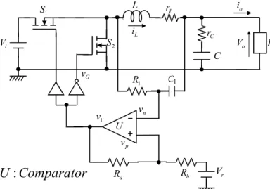
Fig. 3 shows a presented hysteretic PWM controlled buck converter and an error amplifier. The error amplifier is used to provide the voltage to the comparator as a reference and is not needed to have high gain over the switching frequency.
The most peculiar part of the controller is hysteretic comparator part. The triangular voltage vn is obtained from simple RC network connected between the comparator output and the ground. The voltage of positive input of the comparator vp is obtained from output voltage of error amplifier and output voltage of the comparator. The switching frequency of presented controller is basically determined by the time constant TC and the hysteretic
PEDS2009
v1
vp
vn
Vi Vo
vG
S2
L
C R1
Rb
Ra
C1
Comparator
U :
VrrL
S1
U
RL
iL rC
io
VOH
VH
VL
0 0
0 VH
VL
vl
vn
vp
v1
vp
vn
R1
Rb
Ra
C1
Comparator U :1
Vr
amp OP U2: .
Rf
Cf
Ri
Clock U1
U2
RL
io
DC
DC − Converter
vA
window voltage when a clock signal is not applied.
Fig. 1. Circuit diagram of the buck converter controlled by conventional hysteretic PWM controller
Fig. 2. Operating waveforms of hysteretic comparator
Fig. 3 shows key waveforms of hysteretic comparator.
Upper and lower threshold voltage VH and VL are determined by the output voltage of error amplifier vA, comparator high level output voltage VOH, low level output voltage VOL, and resisters Ra Rb as follows expression (1)(2).
OH b a
b A b a
a
H V
R R v R R R V R
+ +
= + (1)
OL b a
b A b a
a
L V
R R v R R R V R
+ +
= + (2) The output voltage of the comparator positive input is VH
when synchronizing with the fixed frequency that set by outside clock signal of the small duty. In this way, switching cycle is determined. On the other hand, when the clock signal is applied to the positive comparator input, its output is forced to high level even before vn reaches VL. Then vn rises up until it reaches VH. Hence the clock signal determines the timing of the turn on of the main switch S1 and the duty ratio
is automatically fixed so as the output voltage becomes nearly Vr. The transfer function of PWM controller is expressed by the following expression.
OH
A V
sT s
V s
V = +
Δ
Δ 1
) (
)
1( (3) During the comparator output voltage vl is high level, the integrated voltage vn of the negative comparator input rises up until it reaches vH. vl is then changed to low level and vn
begins to descend. If the clock signal is applied to the positive comparator input before vn reaches vL, the comparator output is forced to high level.
As dynamic performance of the PWM controller is mainly determined by the time constant TC= R1C1, it is necessary to make a value of TC large in order to obtain good transient performance for external disturbances. However the large time constant TC at the high switching frequency results small amplitude of triangular voltage vn and it may easily lead undesirable irregular switching due to the incoming switching noise. To solve this problem with small time constant, this means with large amplitude of triangular voltage, the output error voltage is amplified and then fed to inverse input of the comparator. In this case, the gain of error amplifier over the switching frequency is not needed to be high. Because the frequency component of the output transient voltage is much lower than that of the switching noise. Therefore the operational amplifier employed to the error amplifier is not necessary to have high GBW.
III. ANALYSIS OF THE CONTROL CIRCUIT
In the previous study [5], the transfer functions of the hysteretic PWM controller a ramp signal as a perturbation of the input signal. Fig. 4 shows key waveforms of hysteretic comparator.
Fig. 3. Circuit diagram of buck converter controlled by proposed hysteretic PWM controller
PEDS2009
t
t
Control voltage
Duty ratio
Δ v
r 00
Δ D T
Clock
VH
vn
OUTPUT PWM
TON TOFF TON TOFF VL
vp
Fig. 4 Key waveforms of hysteretic converter
1
'
T T
2'
v
rΔ
h
r
V
v +
v
rT
1T
2Fig. 5 Waveforms of comparator input voltage
Fig. 6 Variations of reference voltage and duty ratio
A new approach employing a step function as the input
signal is introduced here.
Initially we consider a steady state term of the duty ratio D for the step change of the reference voltage ΔVr. The steady state output voltage changes with same value since the DC gain of the comparator can be considered infinity for the averaged input voltage. The steady state value of the variation of the duty ratio ΔDo is then
i c r
V T D ΔV
≈
Δ 0 (4) Next, a transient term of the duty ratio is examined by the following procedures. When the small step change of the reference voltage occurs at the beginning of the on state of the main switch S1 as shown in Fig. 5, only the duration of on state changes shown by the dotted line in one switching cycle. The transient term of the duty ratio ΔDt shown in Fig.
6 is approximated by
T V
T D V
OH c r t
≈ Δ
Δ (5) Assuming that the switching period T is sufficiently small compared to the time constant, we have
) ) ( ( )
( t
T T t u t
u − − ≈
δ
(6)i r OH
c r
V t V V
T
D≈ΔV +Δ
Δ δ() (7)
Applying the Laplace transform to (7),
) ( )) 1 ( 1
1 ( )
( e V s
T T V
V s V
D c sT r
OH i i
Δ
− +
=
Δ − (8)
The transfer function between the output voltage and the duty ratio is also obtained by considering the feedback network. In the closed loop operation, the voltage vn is fed to the inverse terminal of the comparator and the transfer function of (8) can be then applied by changing its polarity.
The transfer function of the output voltage to duty ratio has a DC component as indicated by (6) and therefore it behaves like an integral compensation. This is the reason why the steady state and the dynamic performances in the low frequency region are improved using the proposed controller.
In the steady state, the following equations are derived.
For the conventional controller,
o L r
o V r I
V = − (9) Where rL is the equivalent series resistance of the inductor.
For the proposed controller,
r
o V
V = (10) From (9) and (10), it is obvious that the proposed controller has no the steady state error while the conventional controller has that induced by the equivalent series resistance of the inductor and the output current.
PEDS2009
IV. EXPERIMENTAL RESULTS
A 5V to 1.2V-10A buck converter with synchronous rectifier is implemented to examine the performance of proposed PWM controller. Table.1 shows the parameters used in these experiments.
A. Frequency Characteristics
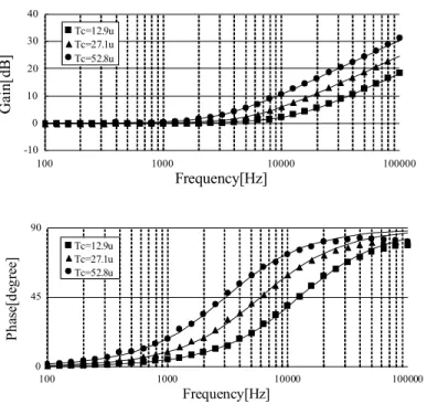
The frequency characteristics of presented PWM controller in free run for three time constants are shown in Fig. 7. This PWM controller has derivative characteristics above the corner frequency determined by time constant TC. And, the frequency characteristics of presented PWM controller in synchronized for three time constants are shown in Fig. 8. Presented PWM controller has derivative characteristics above the corner frequency determined by time constant TC. In this experiment, time constant T is 12μs and corner frequency is 13kHz.The calculated results well agree with the experimental ones.
The frequency characteristics of a operational amplifier are shown in Fig. 9. In this figure, excellent frequency characteristics are achieved.
B. Transient Responses
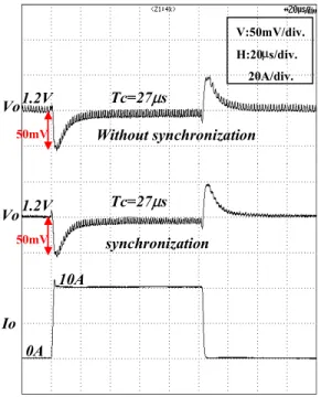
Fig. 10 shows the transient output voltage for the step load change from 0A to 10A with a current slew rate of 10A/ μs.
The top response shows the case without synchronization and second one is that with synchronization. Both responses are almost identical.
C. Load Characteristics
Fig. 11 shows the load characteristics of output voltage and the line characteristics of output voltage. As seen form figure, no steady-state error was observed on the output voltage. It is shown that the proposed controller has the excellent load regulation.
TABLEI
THE VALUE OF EACH ELEMENT
Fig. 7 Frequency characteristic of a PWM control in free run.
(TC =12.9μs,27.1μs,52.8μs, C1=3300pF) symbol value
Vi 5V Vo 1.2V
L 0.36μH
C 400μF
R1 6.2kΩ
C1 3300pF
Ra 100kΩ
Rb 1kΩ
Rf 12kΩ
Cf 560pF
Rs 6.2kΩ
S1 RJK0305 S2 RJK0301 FET-Driver ISL6207 Comparator MAX961
Op-Amp HA17904
-10 0 10 20 30 40
100 1000 10000 100000
Frequency[Hz]
Gain[dB]
Tc=12.9u Tc=27.1u Tc=52.8u
0 45 90
100 1000 10000 100000
Frequency[Hz]
Phase[degree]
Tc=12.9u Tc=27.1u Tc=52.8u
PEDS2009
Fig. 8 Frequency characteristic of a PWM control in synchronized.
(TC =12.9μs,27.1μs,52.8μs, C1=3300pF)
Fig. 9 Frequency characteristic of ΔVA (s)/ ΔVr (s)
V:50mV/div.
H:20μs/div.
20A/div.
Io Vo Vo
50mV
1.2V 1.2V
Tc=27μs Tc=27μs
10A
0A
50mV
synchronization Without synchronization
Fig. 10 Transient responses of the output voltage
Fig. 11 Steady state characteristics
-10 0 10 20 30 40
100 1000 10000 100000
Frequency[Hz]
Gain[dB]
Tc=12.9u Tc=27.1u Tc=52.8u
0 45 90
100 1000 10000 100000
Frequency[Hz]
Phase[degree] Tc=12.9uTc=27.1u
Tc=52.8u
-20 -10 0 10 20
100 1000 10000 100000 1000000 10000000
Frequency[Hz]
Gain[dB]
-270 -225 -180 -135 -90 -45 0 45 90
100 1000 10000 100000 1000000 10000000
Frequency[Hz]
Phase[degree]
1 1.05 1.1 1.15 1.2 1.25 1.3 1.35 1.4
0 2 4 6 8 10
Load current Io[A]
Output voltage Vo[V]
1 1.05 1.1 1.15 1.2 1.25 1.3 1.35 1.4
3 4 5 6 7
Input voltage Vi[V]
Output voltage Vo[V]
PEDS2009
V. CONCLUSION
A new robust PWM control method with inherent derivative characteristics at constant switching frequency is proposed and analyzed. As a result, it was verified that the converter controlled by the proposed PWM method provides excellent transient performances and the stable switching action. The use of small time constant with large gain improve settling time and remove the irregular switching action under the same control bandwidth.
REFERENCES
[1] R. Redl, and N. O. Socal ‘’Near-Optimum Dynamic Regulation of DC- DC Converters Using Feed-Forward of Output Current and Input Voltage with Current-Mde Control,’’ IEEE Trans. On Power Electronics, Vol.PE-1, No.3, 1986, pp. 181-192.
[2] M. T. Zang, M. M Jovanovic and F. C. Lee,’’Analysis and Evaluation of Interleaving Techniques in Forward Converters,’’IEEE Trans. On Power Electronics, Vol.13, No.14, 1998, pp. 690-698.
[3] W. Huang, ’’A New Control for Multi-Phase Buck Converter with Fast Transient Response,’’ Proc. Of Applied Power Electronics Conference, 2001, pp.273-279.
[4] R. Miftakhutdnov, ‘’Analysis and Optimization of Synchronous Buck Converter at High Slew-Rate Load Current Transients,’’Proc. Of Power Electronics Specialalists Conference, 2000, pp. 714-720.
[5] T. Nabeshima T. Sato, S. Yoshida, S. Chiba and K. Onda, ‘’Analysis and Design Considerations of a buck Converter with a hysteretic PWM controller,’’in Proceedings of Power Electronics Specialists Conference, pp. 1711-1716.
PEDS2009