Chapter 2
Design and Analysis of 1x(2N+1) MMI Optical Splitters Based on SOI Rib Waveguide
As mentioned in Chapter 1, the development of integrated optical devices has become the future trend. We propose 1x(2N+1) multimode interference (MMI) optical splitters based on silicon on insulator (SOI) rib waveguide in this chapter. This chapter is organized as follows: Section 2-1 introduces the technique of SOI waveguide and the advantages of the SOI waveguide. The mathematic formulation of beam propagation method (BPM) are also briefly derived and discussed in Section 2-1. Besides we study the directional coupler based on SOI waveguide with and without polymer covered. Section 2-2 introduces the technique of MMI devices.
The advantages of MMI devices applied to integrated optics are presented
and various functions of the MMI structure are also presented. The
mathematic formulation of MMI structure is also briefly described in
Section 2-2. The characteristics of our designed MMI optical splitters based
on SOI rib waveguide by computer-aided beam propagation method software based on BeamPROP_CAD are presented in Section 2-3. We also give the summary of the SOI rib waveguide with polymer covered and our designed 1x(2N+1) MMI optical splitters based on SOI rib waveguide in the final Section 2-4.
2-1 Introduction of the Technique of SOI Waveguide
Silicon waveguide in silicon-on-insulator (SOI) technology is the subject of much investigation due to the SOI technology has much advantage of electronic integrated circuits and photonic integrated circuits (PIC’s) [17-21]. The SOI structure which has the large refractive index difference between Si (n=3.5) and SiO
2(n=1.5) permits that light propagate with the stronger confinement guiding in Si layer, and it can integrate long wavelength photonic devices into the CMOS integrated circuit manufacturing process. Planar and rib optical waveguides formed from silicon-on-insulator (SOI) substrate have been demonstrated propagation losses as low as 1dB/cm in the wavelength range 1.3 to 1.55µm [22-23].
Besides, S. G. Lee et al has demonstrated that SOI devices based on rib
waveguide with polymer cover can be improved power loss in comparison
with the SOI devices based on rib waveguide with air cover at input wavelength 1.55µm [24].
2-1-1 Mathematic Formulation of Beam Propagation Method
In this chapter , we design and simulate the optical SOI waveguide devices based on beam propagation method [25] which is the most commonly used propagation technique for the modeling of integrated photonic devices and fiber-optic devices [26-27]. It is necessary to modeling and optimizing the parameters such as geometry shape, size, polarization state, material data, input wavelength, and output field profile, etc. Because it can avoid the material wasting, save testing time of experiments, and improve realization of the device before we fabricate the device. Besides, we can get some information to modify the device for superior performance according to analyzing the simulation result. The BPM is an approach, which is approximating the exact wave equation for monochromatic waves, and can solve the resulting equations numerically.
Procedures of Finite difference BPM (FD-BPM) are standard numerical
technique [28]. The optical field within one propagation step is calculated
z z z
along the longitudinal coordinate to + ∆ . The electric and magnetic field derived from the Maxwell’s equation can be represented as [29]
t E B
∂
− ∂
=
×
∇ v v
(2-1-1)
t J D
H ∂
+ ∂
=
×
∇ v v v
(2-1-2)
= 0
⋅
∇ D v (2-1-3)
= 0
⋅
∇ B v (2-1-4) where E v is the intensity of the electric field, B v is the flux density of the magnetic field, D v
is flux density of the electric field, H v
is intensity of magnetic field and J v is electric current density. In a source-free Maxwell’s equation J v = 0 , the wave equation under scalar field assumption can be written in the form of the well-known Helmholtz equation for monochromatic waves [30]
( , , )
20
2 2 2 2 2
2
+ Φ =
∂ Φ + ∂
∂ Φ + ∂
∂ Φ
∂ k x y z
z y
x (2-1-5)
The scalar electric field has been written as E ( x , y , z , t ) = Φ ( x , y , x ) e
−iωt, and the notation k = ω ε
0µ
0is for the spatially dependent wavenumber, with
λ π 2
0
=
k is the wavenumber in free space and n ( x , y , z ) is the
refractive index distribution. In typical guided-wave problems the most
rapid variation in the field Φ is the phase variation due to propagation along the guiding axis, and assuming that axis is predominantly along the z direction. Then, Φ ( x , y , z ) is expressed as
) exp(
) , , ( ) , ,
( x y z = u x y z i k z
Φ (2-1-6) where k = k
0n , which is referred to as the reference wavenumber, represents the average variation of Φ ( x , y , z ) and n is reference refractive index. Then, we obtain the following equation for the slowly varying field:
0 ) (
2
2 2 22 2 2 2
2
+ − =
∂ + ∂
∂ + ∂
∂ + ∂
∂
∂ k k u
y u x
u z
k u z i
u (2-1-7)
Assumption the variation of with is sufficiently slow so that the first term above can be neglected with respect to the second. The above equation is reduces to:
u z
⎟⎟ ⎠
⎜⎜ ⎞
⎝
⎛ + −
∂ + ∂
∂
= ∂
∂
∂ k k u
y u x
u k i z
u ( )
2
2 2 2 2 2 2
(2-1-8)
The equation (2-1-8) is the basic formulate for BPM simulations. The
boundary condition we use is the so-called transparent boundary condition
(TBC) [31]. BPM included Polarization effects by recognizing that the
electric field E is a vector, and starting the derivation from the vector wave
equation rather than the scalar Helmholtz equation [32]. The equation
(2-1-8) is formulated in terms of the transverse components of the field ( and ). The equations for the corresponding slowly varying fields ( and ) can be expressed as [32]
E
xE
yu
xu
yy xy x xx
x
A u A u
z
u = +
∂
∂ (2-1-9)
y yy x yx
y
A u A u
z
u = +
∂
∂ (2-1-10)
, where
} ) (
)]
1 ( [ 2 {
2 2 2
2 2
2 x x x
x
xx
u k k u
u y x n n x k u i
A + −
∂ + ∂
∂
∂
∂
= ∂ (2-1-11)
} ) (
)]
1 ( [ 2 {
2 2 2
2 2
y y
y y
yy
n u k k u
y n u y
x k u i
A + −
∂
∂
∂ + ∂
∂
= ∂ (2-1-12)
} )]
1 ( [ 2 {
2 2
2 x x
x
yx
u
x u y
x n n y k u i
A ∂ ∂
− ∂
∂
∂
∂
= ∂ (2-1-13)
} )]
1 ( [ 2 {
2 2
2 y y
x
xx
u
y u x
y n n x k u i
A ∂ ∂
− ∂
∂
∂
∂
= ∂ (2-1-14)
The above equations are generally referred to as describing a full-vectorial BPM.
2-1-2 SOI Single mode Rib Waveguide
The high index difference of SOI wafer can provide strongly guidance in
the rib region of a waveguide for light propagation. Single mode SOI
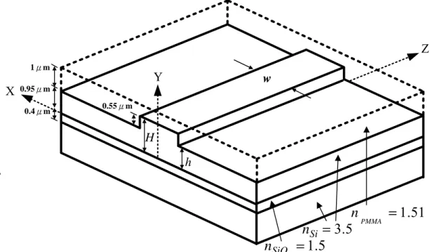
waveguide devices with low propagation losses have been demonstrated at wavelengths λ = 1.3µm and 1.55µm [33-34]. The silicon film thickness is usually 3µm and the buried silicon oxide layer performed as a cladding layer is 1µm thick for standard UNIBOND SOI substrates.
The UNIBOND SOI wafers we used have a 0.4µm buried oxide layer with the refractive index = 1.5 and a 1.5µm crystalline silicon surface
layer with the refractive index = 3.5. The upper surface silicon layer is used to fabricate the waveguide core with an etched rib waveguide. The top cladding layer is air ( = 1) or PolymethylMethacrylate (PMMA) polymer ( = 1.51) for comparing in this section. The design for SOI waveguide single-mode operation should follow the conditions [35]:
sio2
n n si
n
airn
poly⎟⎟ ⎠
⎞
⎜⎜ ⎝
⎛ ⎟
⎠
⎜ ⎞
⎝
− ⎛ +
≤
21 3
. 0
H h H
h H
h (2-1-15)
and
0 . 1 5
.
0 ≤ ≤
H
h (2-1-16)
Fig. 2-1 shows the schematic diagram of our designed UNIBOND SOI
rib waveguide. The width of waveguide w is 6 µm, the slab height is 0.95
µm, and the thickness of the Si guiding layer is 1.5 µm. We use the beam
propagation method to simulate light propagation loss in the SOI rib waveguide. The input light is a Gaussian beam with wavelength 1.55 µm.
The simulation results are shown in Fig. 2-2. In Fig. 2-2, the dashed line presents the normalized intensity of the SOI rib waveguide with air cover.
The normalized intensity of the SOI rib waveguide with polymer cover is presented as a solid line. Both output intensity of the waveguides with air cover and with intensity are normalized to the input power. The output intensity of the rib waveguide with the air cover and with polymer cover is 0.52 and 0.54, respectively. We found that using polymer cover has more propagation intensity about 0.02 than using air cover. The output near field mode pattern of the SOI waveguide with air cover is shown in Fig. 2-2 above the dash line; the output mode pattern of the SOI rib waveguide with PMMA polymer cover is also shown below the solid line. From Fig. 2-2, we can see the mode pattern of the polymer covered waveguide is more approximate to square in comparison with the air covered waveguide. That is to say the waveguide using polymer as cover has a lower propagation loss than using air. Hence, the propagation loss of an SOI rib waveguide can be reduced by using polymer cover.
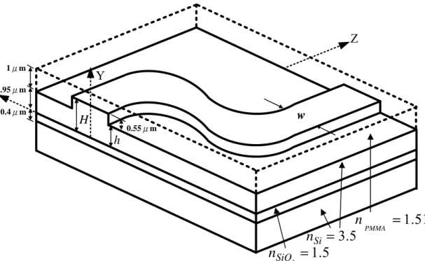
2-1-3 SOI S-Shaped Waveguide
Optical bending waveguides are usually used for changing optical path direction. In general, the optical fibers are connected at the input and output end of SOI waveguide devices. The separation between the two output waveguides must be larger than the centers of the two adjacent fibers. The separation distance typically is 125 to 150µm. The bending loss can be easily suppressed when the corner angle is much smaller than 1 degree [36].
We adopt an S-shaped waveguide connection method in this section. The optical field mismatch at the junction between two arc waveguides can induce a mode conversion loss. To overcome the mode conversion loss, the radius of curvature of the SOI waveguide should be designed as smooth as possible along the light propagation direction. Fig. 2-3 shows the S-shaped waveguide our designed, which has two π/4 radian waveguides with a smooth connection on the UNIBOND SOI wafer.
The lateral offset of the S-shaped waveguide is given by [37]
) ( 2
2 sin
ZZ z X
l Z Z l
X l l
π π +
= (2-1-17)
, where is the length of the S-shaped waveguide, and X and Z are the axes as shown in Fig. 2-3. The output fiber pigtail connections usually need 125 to 150 µm fiber center spacing, which means should be designed for 125 to 150 µm. We design the length as short as possible to reduce
l
Zl
Xl
Xthe connection loss for a certain length l
Z.
The propagation loss of our designed S-shaped SOI waveguides are analyzed by varying the length at length =1 cm. We launched the Gaussian beam as input light wave whose wavelength is 1.55 µm. Fig. 2-4 shows the BPM simulation results of S-shape SOI rib waveguide with and without polymer cover. In Fig. 2-4, the solid line represents the normalized intensity of the S-shaped SOI rib waveguide with air cover and the dashed line represents the normalized intensity of the S-shaped SOI rib waveguide with polymer cover. The output intensity of the rib waveguide with air cover and with polymer cover is 0.51 and 0.53, respectively. We can see clearly that the polymer covered waveguide has the higher output intensity as indicated in Fig. 2-4. After comparing the S-shaped SOI waveguide couplers with and without polymer cover, we find that the insertion loss of the S-shaped waveguide can be improved by 0.1dB/cm when using PMMA polymer cover.
l
Xl
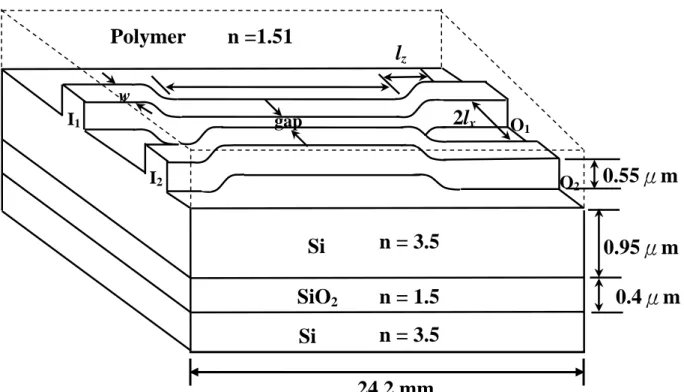
Z2-1-4 SOI Directional Coupler including S-Shaped Waveguide
An optical coupler is one of the key components in passive optical
networks (PON) within fiber-to-the-X (FTTX) communication systems for dividing an optical signal into two or more branches. Therefore, the design of a single mode SOI waveguide device should consider the fiber coupling pigtail connection. We design a UNIBOND SOI directional coupler with four S-shaped bending waveguides for fiber coupling pigtails.
Fig. 2-5 shows the structure of our designed SOI directional coupler. The best set of a single-mode SOI directional waveguide coupler parameters we designed on UNIBOND SOI wafer have a 1.0762µm thick polymer cover, width w=6µm, length =150µm, =1cm, coupling length L=4.2mm, and gap=0.4µm at wavelength 1.55µm. The simulation results are shown in Fig.
2-6. The solid line represents the normalized intensity of the SOI directional coupler with air cover and the dashed line represents the normalized intensity of the SOI directional coupler with polymer cover, respectively. As stated in the previous section, the SOI waveguide with air cover has lower output power, that is, a higher loss. Based on the simulation results, the propagation loss of the polymer covered 2×2 weakly coupling waveguide can be improved.
l
Xl
Z2-2 Introduction of the Technique of MMI Structure
The operation and theory of MMI devices is based on self-imaging effect in the multimode waveguide. Self-imaging is that an input field profile is reproduced in single or multiple images at period in the propagation direction of the guided multimode waveguide [38]. Bryngdahl first proposed the possibility of achieving self-imaging in uniform index slab waveguide [39]. Ulrich made a theoretical and experimental research of the self-imaging properties of dielectric waveguide [40-41].
MMI devices have recently developed into key components for integrated optical circuits. Their advantages, such as stable splitting ratio, compact size, low loss, large optical bandwidth, insensitivity to polarization, good fabrication tolerances [42], and simplicity of production have led to their rapid integration in more complex integrated optical circuits. Several MMI devices have been reported, such as 3dB couplers [43], power splitters [44-45], polarization splitter [46], laser diode [47], electro-optical switch [48], Mach-Zehnder interferometers [49], ring laser [50], and wavelength division multiplexer [51].
2-2-1 Mathematic Formulation of MMI Structure
In this chapter, we design the 1x(2N+1) optical SOI waveguide devices based on beam propagation method which is a particular approach for the modeling and simulation of electromagnetic wave propagation in guided-wave optoelectronic and fiber-optic devices. The beam propagation method is a mathematical method and a propagation technique for the numerical simulation of general optical integrated circuits [52].
The theory describes the light propagation in the MMI section and characteristics of the MMI structure includes the generation of the images.
We do not calculate the absorption of material, extinction ratio, or back reflections at the input and output of access waveguides.
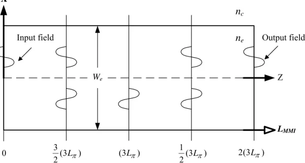
The MMI structure is composed of some single mode waveguides placed at the beginning and its end, and a multimode waveguide placed in the middle region. The geometry of the MMI structure is shown as Fig. 2-7.
Self-imaging is a property of the multimode waveguide as Fig. 2-8. We can get an input field profile in single or multiple images at periodic intervals along the propagation direction of the guided wave in the multimode waveguide.
In a homogeneous multimode waveguide of width a beat length of the two lowest-order modes is defined as [38]
W
eλ β
β π
π
3
4
21 0
e e
W
L ≈ n
= − (2-2-1) where β
0and β
1are the propagation constants of the fundamental mode and first order modes in the step-index multimode waveguide, respectively, λ is the free space wavelength, is the slab effective index at the guiding region, and
n
eW
eis the effective width of the fundamental mode of the multimode guiding waveguide. Note that is slightly larger than . Both
W
eW
MMIn
eand W
eare polarization-dependent. Generally, the beat length corresponding to TE and TM polarizations are not equal for arbitrary waveguide structure. For 1xN optical splitter, the length of multimode can be expressed as [38]
( )
λ π
λ
σ3 ) (
2 5 . 2 0 2 2
⎥ ⎥
⎦
⎤
⎢ ⎢
⎣
⎡ ⎟⎟ ⎠ −
⎜⎜ ⎞
⎝ + ⎛
=
− c e e
c MMI
e
MMI
n n n
W n n
L (2-2-2)
, where σ = 0 for TE wave, and σ = 1 for TM wave.
The excess loss of the 1xN optical splitter is defined as [53]
in i i out
P P Loss
Excess 10 log Σ
_−
= (2-2-3) , where is the intensity of each output port and is the intensity of the input port . The imbalance (or uniformity) of the 1xN optical splitter is defined as [53]
i
P
out_P
inImbalance
max _
min
log
_10
out out
P
− P
= (2-2-4)
, where and are the maximum and minimum intensity of output ports, respectively.
−max
P
outP
out−min2-3 Simulation Results of 1x(2N+1) MMI Optical Splitters Based on SOI Waveguide
The simulation results of 1x(2N+1) MMI optical splitters based on SOI waveguide by computer-aided beam propagation method software based on BeamPROP_CAD for input light wavelength at 1.55µm are shown in this section. The structure of our designed 1x(2N+1) MMI optical splitters is shown as Fig. 2-9. Based on Esq. (2-1-2-1) and (2-1-2-2), we calculate and simulate the single mode waveguide width for SOI wafer. We design the rib waveguide with width w =3µm, rib height H =2.56µm and slab height
=1.69µm for providing single mode operation in input and output waveguides. The length of input single mode waveguide is 100µm and the same length with output single mode waveguide .
h
L
inL
out2-3-1 1 x 3 MMI Optical Splitter
The input single mode rib waveguide is located at the center of the start wall of the MMI section, and the three output single mode rib waveguides are located at W
MMI/ 3 , 0, and − W
MMI/ 3 in the X axes, respectively, on the end wall of the MMI section. We design the multimode waveguide of a 1x3 MMI optical splitter as 18µm. First, we simulate the length characteristics of MMI waveguide. Fig. 2-10 shows the length variation of the multimode waveguide of a 1x3 optical splitter. The excess loss of the device is less than 0.5dB at =241~261µm for TE and TM mode. The uniformity is almost flat and less than 0.01dB at =230~270µm for TE and TM mode. The minimum excess loss of the device is about 0.192dB for TE mode at =251.4µm, and is 0.195dB for TM mode at =251.1µm.
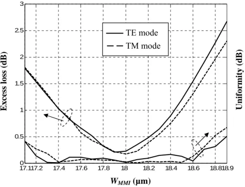
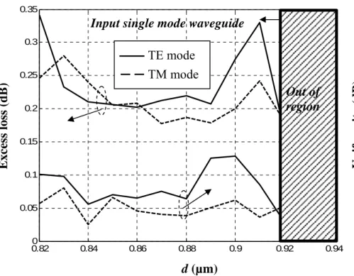
For low polarization dependent loss (PDL), we design the length and width of multimode waveguide of the 1x3 MMI optical splitter as 251.1µm and 18µm, respectively. In the following, we analyze the variation of geometry size and launch wavelength for this 1x3 MMI optical splitter. Fig. 2-11 shows the width variation of multimode interference waveguide. When the width of MMI waveguide is between 17.5µm and 18.45µm, we can see that excess loss is less than 1dB and uniformity is less than 0.085dB. The mean
L
MMIL
MMIL
MMIL
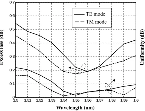
MMITM mode. In Fig. 2-12, we analyze the variation of rib part (the etched depth ) on our designed device. When the etched depth is between 0.82µm to 0.918µm, excess loss of the device is less than 0.28dB and uniformity of the device is less than 0.07dB. The mean value of excess loss of the device for TE mode and TM mode is about 0.21dB and 0.20dB, respectively. The mean value of uniformity of the device about TE mode and TM mode is 0.05dB and 0.03dB, respectively. Fig. 2-13 shows the response of input light wavelength of this 1x3 MMI optical splitter. The excess loss of this 1x3 MMI optical splitter is less than 0.54dB and the uniformity is less than 0.21dB at input wavelength between 1.5µm and 1.6µm for TE and TM mode.
d
2-3-2 1 x 5 MMI Optical Splitter
The input single mode rib waveguide is located at the center of the start
wall of the MMI section, and the five output single mode rib waveguides
are located at 2 W
MMI/ 5 , W
MMI/ 5 , 0, − W
MMI/ 5 and − 2 W
MMI/ 5 in the X
axes, respectively, on the end wall of the MMI section. We design the
multimode waveguide of a 1x5 MMI optical splitter as 30µm. First, we
simulate the length characteristics of MMI waveguide. Fig. 2-14 shows the
length variation of the multimode waveguide of the 1x5 optical splitter. The
excess loss of the device is less than 0.55dB at = 404.5~424.7µm for TE and TM mode. The uniformity is almost flat and less than 0.03dB at
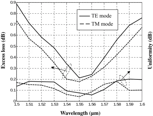
=393~430µm for TE and TM mode. The minimum excess loss of the device is 0.196dB for TE mode at =415.5µm, and is 0.194dB for TM mode at =414µm. For PDL, we design the length and width of multimode waveguide of the 1x5 MMI optical splitter as 414.6µm and 30µm, respectively. In the following, we analyze the variation of geometry size and launch wavelength for the 1x5 MMI optical splitter. Fig. 2-15 shows the width variation of multimode interference waveguide. When the width of MMI waveguide is between 29.7µm and 30.3µm, we can see that excess loss is less than 0.6dB and uniformity is less than 0.29dB. The mean value of uniformity is about 0.15dB for TE mode and is about 0.12dB for TM mode. In Fig. 2-16, we analyze the variation of rib part (the etched depth ) on our designed device. When the etched depth is between 0.82µm to 0.918µm, excess loss of the device is less than 0.34dB and uniformity of the device is less than 0.13dB. The mean value of excess loss of the device for TE mode and TM mode is about 0.24dB and 0.21dB, respectively. The mean value of uniformity of the device about TE mode and TM mode is 0.08dB and 0.05dB, respectively. Fig. 2-17 shows the response of input light wavelength of 1x5 MMI optical splitter. The excess loss of this 1x5 MMI optical splitter is less than 0.89dB and the uniformity
L
MMIL
MMIL
MMIL
MMId
is less than 0.21dB at input wavelength between 1.5µm and 1.6µm for TE and TM mode.
2-3-3 1 x 7 MMI Optical Splitter
The input single mode rib waveguide is located at the center of the start wall of the MMI section, and the five output single mode rib waveguides are located at 3 W
MMI/ 7 , , , 0, 2 W
MMI/ 7 W
MMI/ 7 − W
MMI/ 7 , and
in the X axes, respectively, on the end wall of the MMI section.
We design the multimode waveguide of a 1x7 MMI optical splitter as 42µm.
First, we simulate the length characteristics of MMI waveguide. Fig. 2-18 shows the length variation of the multimode waveguide of the 1x7 optical splitter. The excess loss of the device is less than 0.6dB at
=566.3~588µm for TE and TM mode. The uniformity is almost flat and less than 0.05dB at =552~595µm for TE and TM mode. The minimum excess loss of the device is 0.197dB for TE mode at
=578.1µm, and is 0.195dB for TM mode at =576.2µm. For low PDL, we design the length and width of multimode waveguide of the 1x7 MMI optical splitter as 577.1µm and 42µm, respectively. In the following, we analyze the variation of geometry size and launch wavelength for the 1x7 MMI optical splitter. Fig. 2-19 shows the width variation of multimode
7 / 2 W
MMI− 7
/ 3 W
MMI−
L
MMIL
MMIL
MMIL
MMIinterference waveguide. When the width of MMI waveguide is between 41.58µm and 42.42µm, we can see that excess loss is less than 0.94dB and uniformity is less than 0.31dB. The mean value of uniformity is about 0.17dB for TE mode and is about 0.13dB for TM mode. In Fig. 2-20, we analyze the variation of rib part (the etched depth ) on our designed device. When the etched depth is between 0.82µm to 0.918µm, excess loss of the device is less than 0.41dB and uniformity of the device is less than 0.18dB. The mean value of excess loss of the device for TE mode and TM mode is about 0.26dB and 0.23dB, respectively. The mean value of uniformity of the device about TE mode and TM mode is 0.09dB and 0.06dB, respectively. Fig. 2-21 shows the response of input light wavelength of the 1x7 MMI optical splitter. The excess loss of this 1x7 MMI optical splitter is less than 1.4dB and the uniformity is less than 0.88dB at input wavelength between 1.5µm and 1.6µm for TE and TM mode.
d
2-3-4 1 x 9 MMI Optical Splitter
The input single mode rib waveguide is located at the center of the start
wall of the MMI section, and the five output single mode rib waveguides
are located at 4 W / 9 , 3 W / 9 , 2 W / 9 , W / 9 , 0, − W / 9 ,
9 / 2 W
MMI− , − 3 W
MMI/ 9 and − 4 W
MMI/ 9 in the X axes, respectively, on the end wall of the MMI section. We design the multimode waveguide of a 1x9 MMI optical splitter as 54µm. First, we simulate the length characteristics of MMI waveguide for the 1x9 MMI optical splitter. Fig.
2-22 shows the length variation of the multimode waveguide of the 1x9 optical splitter. The excess loss of the device is less than 0.65dB at = 728.1~751.4µm for TE and TM mode. The uniformity is almost flat and less than 0.07dB at =718~758µm for TE and TM mode. The minimum excess loss of the device is 0.197dB for TE mode at
=740.8µm, and is 0.195dB for TM mode at =739.2µm. For low polarization dependent loss (PDL), we design the length and width of multimode waveguide of the 1x9 MMI optical splitter as 739.7µm and 54µm. In the following, we analyze the variation of geometry size and launch wavelength for the 1x9 MMI optical splitter. Fig. 2-23 shows the width variation of multimode interference waveguide of the 1x9 MMI optical splitter. When the width of MMI waveguide is between 53.46µm and 54.54µm, we can see that excess loss is less than 1.4dB and uniformity is less than 0.66dB. The mean value of uniformity is about 0.39dB for TE mode and is about 0.31dB for TM mode. In Fig. 2-24, we analyze the variation of rib part (the etched depth ) on our designed 1x9 MMI optical splitter. When the etched depth is between 0.82µm to 0.918µm, excess loss
L
MMIL
MMIL
MMIL
MMId
of the device is less than 0.47dB and uniformity of the device is less than 0.20dB. The mean value of excess loss of the device for TE mode and TM mode is about 0.30dB and 0.26dB, respectively. The mean value of uniformity of the device about TE mode and TM mode is 0.10dB and 0.07dB, respectively. Fig. 2-25 shows the response of input light wavelength of the 1x9 MMI optical splitter. The excess loss of this 1x9 MMI optical splitter is less than 2.1dB and the uniformity is less than 1.5dB at input wavelength between 1.5µm and 1.6µm for TE and TM mode.
2-4 Summary
In this chapter, we design optical SOI waveguide devices including
straight rib waveguide, S-shaped waveguide, directional waveguide coupler
with and without PMMA polymer cover, and 1x(2N+1) optical MMI
splitter. The propagation losses of the integrated optical SOI waveguide
devices with or without PMMA polymer cover are compared. From the
above simulation studies, we found that using a polymer cover can enhance
the total optical power transmission with a proper Gaussian beam launched
into the SOI rib waveguide devices, That is, the guided-wave propagated
along SOI waveguide devices with polymer cover effectively has a larger core with the input light mode spot size fixed. The power loss can be improved with just 1 µm thick PMMA polymer cover. Such a basic study is helpful for SOI VLSI photonic devices fabrication.
The 1x(2N+1) optical MMI splitter based on SOI rib waveguide our designed based on low PDL. When the length of multimode waveguide of our designed 1x(2N+1) optical splitter based on the SOI rib waveguide add or subtract 10µm, the relation of L
MMIand the number of output ports for 1x(2N+1) optical splitter based on SOI rib waveguide is shown in Fig. 2-26.
When the width of multimode waveguide of our designed 1x(2N+1) optical splitter based on the SOI rib waveguide add or subtract , the relation of
W
MMI01 . 0
W
MMIand the number of output ports for 1x(2N+1) optical
splitter based on SOI rib waveguide is shown in Fig. 2-27. The relation of
the etched depth of SOI rib waveguide and the number of output ports for
our designed 1x(2N+1) optical splitter based on SOI rib waveguide is
shown in Fig. 2-28. The relation of input light wavelength response and the
number of output ports for our designed 1x(2N+1) optical splitter based on
SOI rib waveguide is shown in Fig. 2-29.
Fig. 2-1 Structure of optical SOI rib waveguide
5 .
2
= 1 n
SiO5 .
= 3 n
Si51 .
= 1 n
PMMAh
0.55μm
H
Z Y w
1μm
0.4μm 0.95μm
X
`
2 4 6 8 10 12
0.4 0.45 0.5 0.55 0.6 0.65 0.7 0.75 0.8
Without polymer cover With polymer cover
Normalized Intensity (a.u)
Propagation length (mm)
Fig. 2-2 Simulation results of power propagation and mode pattern
of an SOI straight rib waveguide with and without
polymer
Z
X
0.95μmY
5 .
2
= 1 n
SiO5 .
= 3 n
Si51 .
= 1 n
PMMAH w
0.55μm
h
1μm
0.4μm
Fig. 2-3 Structure of optical SOI S-shaped waveguide.
1.6 3.2 4.8 6.4 8 9.6 10
0.4 0.45 0.5 0.55 0.6 0.65 0.7 0.75 0.8
With polymer cover Without polymer cover
Normalized Intensity (a.u.)
Propagation length (mm)
Fig. 2-4 Simulation results of power propagation and mode pattern of an
SOI S-shaped rib waveguide with and without polymer
24.2 mm n = 3.5 Si
Si n = 3.5
SiO
2n = 1.5 2l
xl
zgap w
0.55μm
0.95μm 0.4μm I
1O
2O
1I
2Polymer n =1.51
Fig. 2-5 Structure of the whole SOI directional waveguide coupler including S-bend power splitting branches with polymer cover
5 10 15 20 24.2
0 0.1 0.2 0.3 0.4 0.5 0.6 0.7
Without polymer cover With polymer cover
O
2O
1I
1Normalized Intensity (a.u.)
I
2Propagation length (mm)
Fig. 2-6 Simulation results of power propagation and mode pattern of an SOI
directional waveguide coupler including S-bend power with and
Multimode waveguide W
MMIL
MMI●
●
●
●
●
●
Output single mode waveguides Input single mode waveguides
Fig. 2-7 Structure of MMI devices
Z X
Input field n
eOutput field
L
MMI)
3 2 (
1 L
π) 3 ( L
π)
3 2 (
3 L
π2 ( 3 L
π)
n
cW
e0
Fig. 2-8 Multimode waveguide based on Self-imaging
X Y
Output
5 .
2
= 1 n
SiO5 .
= 3 n
SiZ
Input
Fig. 2-9 Structure of 1x(2N+1) MMI optical splitter based on SOI rib waveguide
TE mode TM mode
Uniformity (dB)
L
MMI(µm)
Excess loss (dB)
Fig. 2-10 Length variation of MMI waveguide of a 1x3
MMI splitter with W
MMI=18µm and d=0.87µm at
input wavelength 1.55µm
17.117.20 17.4 17.6 17.8 18 18.2 18.4 18.6 18.818.9 0.5
1 1.5 2 2.5 3
TE mode TM mode
Uniformity (dB)
Excess loss (dB)
W
MMI(µm)
Fig. 2-11 Width variation of MMI waveguide of a 1x3 MMI splitter with L
MMI=251.1µm and d=0.87µm at input wavelength 1.55µm
0.820 0.84 0.86 0.88 0.9 0.92 0.94
0.05 0.1 0.15 0.2 0.25 0.3 0.35
TE mode TM mode
Out of region Input single mode waveguide
Uniformity (dB)
Excess loss (dB)
d (µm)
Fig. 2-12 Etched depth variation of rib waveguide of a 1x3
MMI splitter with L
MMI=251.1µm and W
MMI=18µm
at input wavelength 1.55µm
1.5 1.51 1.52 1.53 1.54 1.55 1.56 1.57 1.58 1.59 1.6 0
0.1 0.2 0.3 0.4 0.5 0.6 0.7
TE mode TM mode
Uniformity (dB)
Excess loss (dB)
Wavelength (µm)
Fig. 2-13 Response of input wavelength of a 1x3 MMI splitter with L
MMI=251.1µm, W
MMI=18µm and d=0.87µm
370 380 390 400 410 420 430 440 450
0 0.5 1 1.5 2 2.5 3 3.5
TE mode TM mode
Uniformity (dB)
Excess loss (dB)
L
MMI(µm)
Fig. 2-14 Length variation of MMI waveguide of a 1x5
MMI splitter with W
MMI=30µm and d=0.87µm at
input wavelength 1.55µm
28.50 29 29.5 30 30.5 31 31.5 0.5
1 1.5 2 2.5 3 3.5 4 4.5
Uniformity (dB)
Excess loss (dB)
W
MMI(µm)
Fig. 2-15 Width variation of MMI waveguide of a 1x5 MMI splitter with L
MMI=414.6µm and d=0.87µm at input wavelength 1.55µm
TE mode TM mode
0.820 0.84 0.86 0.88 0.9 0.92 0.94
0.05 0.1 0.15 0.2 0.25 0.3 0.35
TE mode TM mode
Input single mode waveguide
Out of region
Uniformity (dB)
Excess loss (dB)
d (µm)
Fig. 2-16 Etched depth variation of rib waveguide of a 1x5
MMI splitter with L
MMI=414.6µm and W
MMI=30µm
at input wavelength 1.55µm
1.5 1.51 1.52 1.53 1.54 1.55 1.56 1.57 1.58 1.59 1.6 0
0.1 0.2 0.3 0.4 0.5 0.6 0.7 0.8 0.9
TE mode TM mode
Uniformity (dB)
Excess loss (dB)
Wavelength (µm)
Fig. 2-17 Response of input wavelength of a 1x5 MMI splitter with L
MMI=414.6µm, W
MMI=30µm and d=0.87µm
530 540 550 560 570 580 590 600 610
0 0.5 1 1.5 2 2.5 3 3.5 4
TE mode TM mode
Uniformity (dB)
Excess loss (dB)
L
MMI(µm)
Fig. 2-18 Length variation of MMI waveguide of a 1x7
MMI splitter with W
MMI=42µm and d=0.87µm at
input wavelength 1.55µm
40 40.5 41 41.5 42 42.5 43 43.5 44 0
1 2 3 4 5 6
TE mode TM mode
Uniformity (dB)
Excess loss (dB)
W
MMI(µm)
Fig. 2-19 Width variation of MMI waveguide of a 1 x 7 MMI splitter with L
MMI=577.1µm and d=0.87µm at input wavelength 1.55µm
0.820 0.84 0.86 0.88 0.9 0.92 0.94
0.05 0.1 0.15 0.2 0.25 0.3 0.35 0.4 0.45
TE mode TM mode
Out of region Input single mode waveguide
Uniformity (dB)
Excess loss (dB)
d (µm)
Fig. 2-20 Etched depth variation of rib waveguide of a 1 x 7
MMI splitter with L
MMI=577.1µm and W
MMI=42µm
at input wavelength 1.55µm
1.5 1.51 1.52 1.53 1.54 1.55 1.56 1.57 1.58 1.59 1.6 0
0.25 0.5 0.75 1 1.25 1.5
TE mode TM mode
Uniformity (dB)
Excess loss (dB)
Wavelength (µm)
Fig. 2-21 Response of input wavelength of a 1x7 MMI splitter with L
MMI=577.1µm, W
MMI=42µm and d=0.87µm
700 710 720 730 740 750 760 770 780
0 0.5 1 1.5 2 2.5 3 3.5
TE mode TM mode
Uniformity (dB)
Excess loss (dB)
L
MMI(µm)
Fig. 2-22 Length variation of MMI waveguide of a 1 x 9
MMI splitter with W
MMI=54µm and d=0.87µm at
input wavelength 1.55µm
51.5 52 52.5 53 53.5 54 54.5 55 55.5 56 56.5 0
2.5 5 7.5 10 12.5 15
TE mode TM mode
Uniformity (dB)
Excess loss (dB)
W
MMI(µm)
Fig. 2-23 Width variation of MMI waveguide of a 1 x 9 MMI splitter with L
MMI=739.7µm and d=0.87µm at input wavelength 1.55µm
0.820 0.84 0.86 0.88 0.9 0.92 0.94
0.05 0.1 0.15 0.2 0.25 0.3 0.35 0.4 0.45 0.5
TE mode TM mode
Out of region Input single mode waveguide
Uniformity (dB)
Excess loss (dB)
d (µm)
Fig. 2-24 Etched depth variation of rib waveguide of a 1 x 9
MMI splitter with L
MMI=739.7µm and W
MMI=54µm
at input wavelength 1.55µm
1.5 1.51 1.52 1.53 1.54 1.55 1.56 1.57 1.58 1.59 1.6 0
0.5 1 1.5 2 2.5