60-GHz CMOS Integrated On-Chip Yagi Antenna and Balun Bandpass Filter in 90-nm CMOS Technology
Han-Lin Yue, Yung-Hsiang Chuang, and Huey-Ru Chuang
Institute of Computer and Communication Engineering, Department of Electrical Engineering, National Cheng Kung University,
Tainan, Taiwan, R.O.C Abstract—This paper presents the design of a 60-GHz CMOS
integrated on-chip Yagi antenna with balun bandpass filter by using 90-nm CMOS technology. The Yagi antenna is fed by the balanced output of the balun bandpass filter, whose amplitude and phase differences between the balance ports from 57 to 64 GHz are within 1.3 dB and 180° ± 5°, respectively. The effect of the metallic plane of the probe station has been considered in the calculation of the antenna power gain from the Friis power transmission formula with two identical face-to-face antenna- balun-filters. The measured antenna-balun-filter power gain is - 12.4 dBi at 60 GHz.
Keywords-60 GHz; Yagi antenna; on-chip antenna; balun filter;
bandpass filter; complementary metal–oxide–semiconductor(CMOS)
I. INTRODUCTION
In order to pursue the mm-wave single-chip RF transceiver and antenna integration, mm-wave on-chip antennas and bandpass filters have been studied [1]-[3]. Recently, multifunction mm-wave components have been developed that can combine different functions into one device and further simplify the complexity of the RF front-end circuits [2]. In this paper, a CMOS on-chip integration of a 60-GHz Yagi antenna and a balun bandpass filter is presented. The on-wafer measurement of the input VSWR and the power gain of the integrated antenna-balun-filter are conducted on a probe station.
The effect of the metallic plane of the probe station has been considered in the calculation of the antenna power gain from the Friis power transmission formula with two identical face- to-face antenna-balun-filters. The good agreement is observed.
The designed integrated on-chip antenna-balun-filter can be very useful for the integrated design of the 60-GHz CMOS single-chip RF transceiver.
II. INTEGRATED ON-CHIP ANTENNA AND BALUN-FILTER A. Yagi-Antenna Design
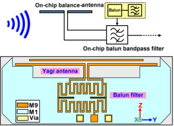
Fig. 1 shows the schematic of the designed integrated CMOS on-chip Yagi antenna and balun bandpass filter. The Yagi antenna consists of a director element, a driven element, and a reflector element. For the Yagi antenna design, except the reflector element on the bottom-metal-layer (M1), all others are on the top-metal-layer (M9). The driven element is fed by the balanced output of the balun bandpass filter. The length of the driven, director, and reflector elements are around 0.5 λeff, 0.45 λeff, and 0.6 λeff, respectively. Here, λeff is the effective wavelength of the silicon substrate at 60 GHz.
Figure 1. Schematics of the designed 60-GHz CMOS on-chip integrated Yagi antenna and balun bandpass filter.
B. Balun Bandpass Filter Design
The proposed balun bandpass filter is composed of two open loop resonators with coupled sections and three feeding lines [2]. The coupled-line section with open circuited terminal is equivalent to a J-inverter, and the length of the open loop resonators is nearly half a wavelength.
For phase analysis of the balanced port, the three-port network can be simplified into a two-port network when the 50-Ω load is terminated at one of the three ports. Furthermore, the transmission coefficient between two unloaded ports can be calculated from the total Y-parameter matrix. To operate at mm-wave frequency range, preventing the currents from being injected into the substrate and reducing the transmission loss are crucial in a CMOS-based device. The ground plane is arranged as the bottom-metal-layer (M1), and the signal line is used as the top-metal-layer (M9); this forms a microstrip structure. Base on the above analysis, a balun bandpass filter is designed.
III. SIMULATION AND MEASUREMENT RESULTS
The simulated result of the balun bandpass filter is shown in Fig. 2. The magnitude of S21 at the center frequency is about -6.2 dB, including a 3-dB splitting loss, and the magnitude of S11 is better than -10 dB. The simulation results for the amplitude and phase differences between the balance ports from 57 to 64 GHz are within 1.3 dB and 180° ± 5°, respectively.
0 10 20 30 40 50 60 70 80 90 100 110 Frequency (GHz)
-30 -25 -20 -15 -10 -5 0
Magnitude (dB)
S(1,1) S(2,1) S(3,1)
Figure 2. Simulated results of designed 60 GHz balun bandpass filter.
Figure 3. Chip micrograph (chip size = 1.16 × 0.44 mm2)
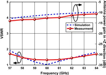
Fig. 3 is the chip micrograph of the fabricated integrated CMOS antenna–balun-filter with a chip size of 1.16 × 0.44 mm2. Fig. 4 shows the comparison between simulation and measurement of the designed 60-GHz CMOS integrated on- chip Yagi antenna and balun bandpass filter. A good agreement is obtained. The input VSWR is less than 2 from 57 to 64 GHz.
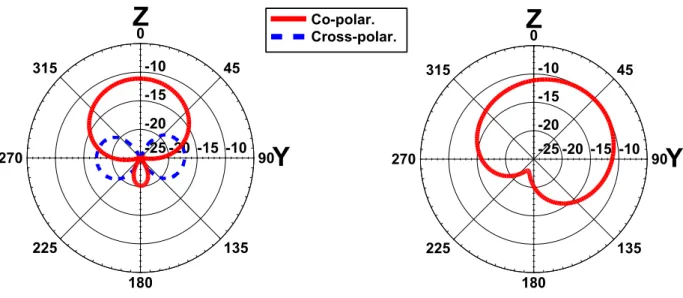
The simulated radiation patterns are shown in Fig. 5. It is noted that the resemblance of the simulated antenna patterns in Fig. 5 coincides with the broadside pattern characteristics of the Yagi antenna.
The power gain of the antenna was measured with the technique presented in [3] and [4]. As shown in Fig. 6, two identical on-chip antennas located on the probe station are placed face-to-face with a distance R (R = 20 mm is this case), which should be satisfied with the far-field condition. In this setup, one antenna is used as a transmitting antenna and the other as a receiving antenna. It should be noted that in the practical measurement environment, the effect of the metal chuck on the microwave probe station, which acts like a metallic ground plane, should be considered in the antenna power gain measurement. This issue can be treated like both the transmitting and receiving antennas are located above a perfectly conducting ground plane. According to the above measurement procedure, the power gain of the on-chip antenna can be extracted from the measured S21. As shown in Fig. 4, it is observed that the simulated and measured Z-direction power gains are in good agreement. The measured antenna-balun- filter power gain is -12.4 dBi at 60 GHz.
57 58 59 60 61 62 63 64
Frequency (GHz) 1
2 3 4 5
VSWR
-35 -30 -25 -20 -15 -10 -5 Bi)ain + (dntiocire dZ inr gewonA pannte
Simulation Measurment
Figure 4. Simulated and measured input VSWR and power gain
IV. CONCLUSION
A successful integration of a 60-GHz CMOS integrated on- chip Yagi antenna with balun bandpass filter has been reported.
An on-chip antenna-balun-filter is fabricated with 90-nm CMOS technology. The Yagi antenna is fed by the balanced output of the balun bandpass filter, whose amplitude and phase differences between the balance ports from 57 to 64 GHz are within 1.3 dB and 180° ± 5°, respectively. The effect of the metallic plane of the probe station has been considered in the calculation of the antenna power gain from the Friis power transmission formula with two identical face-to-face antenna- balun-filters. The simulation and measurement results are in good agreement. The input VSWR is less than 2 within 57 to 64 GHz and the antenna power gain is -12.4 dBi at 60 GHz.
The designed CMOS integrated on-chip antenna-balun-filter is useful for the integrated design of a 60-GHz single-chip RF transceiver.
V. REFERENCE
[1] Y. P. Zhang, M. Sum, and L. H. Guo, “On-chip antennas for 60-GHz radios in silicon technology,” IEEE Trans. Electron Devices, vol. 52, no.
7, pp. 1664–1668, Jul. 2005.
[2] C.-Y. Hsu, C.-Y. Chen, and H.-R. Chuang, “A 77-GHz CMOS on-chip bandpass filter with balanced and unbalanced outputs,” IEEE Electron Device Lett., vol. 31, no.11, pp. 1205–1207, Nov. 2010.
[3] H.-R. Chuang, L.-K. Yeh, P.-C. Kuo, K.-H. Tsai, H.-L. Yue, “60-GHz millimeter-wave CMOS integrated on-chip antenna and bandpass filter"
IEEE Trans. on Electron Devices, vol. 58, no. 7, pp. 1837–1845, July 2011.
[4] R. N. Simionsand R. Q. Lee, “On-wafer characterization of millimeter wave antennas for wireless application,” IEEE Trans. Microw. Theory Tech., vol. 47, no. 1, pp. 92–96, Jan. 1999.
[5] C. A. Balanis, Antenna Theory and Design., 3rd ed. New York: Wiley, 2005, ch. 10.
[6] S. R. Saunders, Antennas and propagation for wireless communication systems. New York: Wiley, 1999, ch5, pp.94–97.
0
45
90
135 180
225 270
315 -10
-10 -15
-15 -20
-20 -25
Z
Y
0
45
90
135 180
225 270
315 -10
-10 -15
-15 -20
-20 -25
Z
Y
Figure 5. Simulated radiation patterns in YZ- and XZ-plane at 60 GHz.
Figure 6. Illustration of the on-wafer setup for the power gain measurement of the on-chip antenna in a microwave probe station.
Co-polar.
Cross-polar.