行政院國家科學委員會專題研究計畫 成果報告
5GHz 無線區域網路 SiGe HBT 收發機射頻前端電路設計
(3/3)
計畫類別: 個別型計畫
計畫編號: NSC94-2215-E-006-061-
執行期間: 94 年 08 月 01 日至 95 年 07 月 31 日
執行單位: 國立成功大學微電子工程研究所
計畫主持人: 陳志方
共同主持人: 莊英宗
計畫參與人員: 林建勳、蘇國彰、吳明憲、陳和謙
報告類型: 完整報告
報告附件: 出席國際會議研究心得報告及發表論文
處理方式: 本計畫可公開查詢
中 華 民 國 95 年 8 月 3 日
5GHz 無線區域網路 SiGe HBT 收發機射頻前端電路設計(3/3)
Design of the SiGe HBT transceiver for 5 GHz Wireless LAN applications
計畫編號:NSC94-2215-E-006-061
執行期間:94 年 8 月 1 日 至 95 年 7 月 31 日
主持人:陳志方
國立成功大學微電子所副教授
一、中文摘要
在本計劃中,我們探討各種元件的不同佈局、大 小變化對於元件特性的影響。對於低雜訊放大器之應 用,利用射極尺寸的變化去使得最佳的雜訊與輸入阻抗 皆接近於 50 歐姆,並得到最佳的元件用於低雜訊應 用,以便於在製作低雜訊放大器時能夠簡化匹配網路並 減少其損耗。藉由小信號雜訊等效模型,推導得到相關 參數間的關係式與其萃取值,最後得到一最佳主動元件 尺寸、低雜訊之佈局最佳化與最佳偏壓點。此外,也完 成一個針對應用於 WLAN IEEE 802.11a 射頻功率放 大器之高功率power cell 之佈局最佳化。此經過改良的 power cell 佈局,可以有效減少受到非理想因素的干擾 影響,使得此改良過後的 power cell 的特性比一般的 power cell 特性更佳。 我們設計一適用於IEEE 802.11a 無線區域網路 應用之線性化矽鍺功率放大器,此線性化電路有效的改 善電路線性而幾乎不會增加直流電源損耗與晶片面 積。此外,此雙極功率放大器使用主動偏壓電路,並使 功率放大器操作在低靜態偏壓的 Class AB。在本計劃 中,我們也設計了一操作於 5.2 GHz 的高積體化的低 雜訊放大器。此外,我們也設計了一適用於 WLAN IEEE 802.11a 的混波器與壓控振盪器。英文摘要
In this project, the impacts of various layout configuration and device dimensions on the device performance are examined. For low noise amplifiers (LNAs), the geometrical scaling issues including emitter length and emitter stripe-number scaling are used to shift simultaneously the optimum noise and optimum source
impedance to a point which is close to 50 Ω. Via this method, not only the optimal transistor size for low noise applications is obtained, but the matching network is simplified to reduce the losses of passive networks and the chip area. Expressions of noise parameters are derived via the small signal noise equivalent model, and these parameters are extract. Based on experimental results, optimum device size, layout of low noise cell, and bias suitable for LNAs are determined. In addition, a novel SiGe HBT power cell for wireless LAN IEEE 802.11a power amplifier (PA) applications is proposed. The subcells with different emitter stripe widths have been compared. Besides, the layout of a novel power cell is designed and optimized to alleviate non–ideal effects for better performance. Compared with performance of power cells, it is demonstrated that this novel power cell is superior to other power cells for the design of the PA.
A highly linear SiGe power amplifier for IEEE 802.11a Wireless LAN applications has been demonstrated by adopting a new integrated on-chip linearizer. The proposed linearizer, consisting of SiGe heterojunction bipolar (HBT) active bias circuit partially coupled to RF input power together with a coupling reverse-biased diode, effectively improves linearity with no additional dc consumption and die area. The two-stage power amplifier operates with a low quiescent current of Class AB mode using active bias circuit. Furthermore, a high integrated 5.2 GHz inductively degenerated cascode low noise amplifier (LNA) also has been realized in this project. Moreover, a Mixer and a VCO (voltage-controlled oscillator) for IEEE
802.11a Wireless LAN applications are also demonstrated in this work.
二、計畫的緣由與目的
Nowadays, numerous wireless-communication circuit applications, especially for low-noise amplifiers (LNAs), often require transistors with low noise. In addition to providing the gain, LNA should minimize signal distribution, present a specific impedance (e.g., 50 Ω) to the input source, and consume as small power as possible. SiGe HBT technology has been a chief contender among the Si-based technology due to its advantages over CMOS technology such as higher fT, lower noise, and
better power performance. The performance of SiGe HBTs is depended on many factors including the Ge profile, the doping concentration, and the geometrical structure. More attention should be paid to the noise figure (NF) and the associated available gain (GA,assoc) if HBTs are employed
in the LNA, and therefore the geometry and bias need to be optimized for the LNA design. Geometrical scaling issues including emitter length and emitter stripe-number scaling are investigated from an RF design perspective. Since substrate losses are considerably higher in Si, the attention should be focused on optimizing the sizes of transistors in order to simplify the matching circuit, rather than designing new matching circuit to match a given transistor. Therefore, the real part of the optimum source impedance (Re(Zopt)) of a transistor close to 50 Ω is selected for
designing a Si-base LNA. In this way, the loss and even the chip area can be reduced. For devices with the fixed vertical doping concentration and Ge profile, the noise performance of SiGe HBTs is investigated and the optimal device geometry is determined to render a better noise performance. The details of the device performance, and the effects of layout configuration and dimensions are discussed. In addition, a method is proposed to optimize the emitter geometry in order to minimize the matching circuit losses and noise figure.
The wireless communication market, such as wireless LAN (WLAN), has experienced a substantial and rapid growth. Due to SiGe HBTs feature comparable RF performance to that of III–V HBTs and low fabrication cost, SiGe HBTs are emerging as a contender for RF power amplifier (PA) applications. Since the PA is the most essential component in the RF transceiver, and the power cell determines the performance of the PA, hence, it’s very important to design a power cell with high power-added efficiency (PAE), power gain (GP), and
linearity. Therefore, considering temperature effects and the desired high power level, it’s required to carefully design the layout of a power cell to maintain adequate gain and PAE. Due to the PA needs greater output power (Pout),
the power cell of the PA is composed of an array of multifinger subcells (i.e. several unit-devices in parallel). For the ideal case, subcells are combined perfectly, the Pout
of the power cell is proportional to numbers of subcells, and the GP of the power cell keeps the same as that of a
subcell. In fact, this ideal case can not be realized due to non-ideal effects including thermal effects associated with the thermal coupling between subcells/ stripes, the common inductance associated with the emitter lead, and inter-subcell phasing effects associated with the base-feed. There are some basic and familiar styles of power cells shown in literatures. However, these styles of power cells are still suffered from non-ideal effects. Hence, the objective in this work is to design an optimized and novel power cell with better performance than these styles of power cells. Moreover, this proposed power cell is designed to be suitable for circuit-level combination in PAs for WLAN IEEE 802.11a applications.
The demand for wireless data transmission is increasing rapidly. While the 2.4 GHz band is already crowded, systems in the 5 GHz ISM band are increasing. As new WLAN (Wireless LAN) standards emerge, such as IEEE 802.11a, additional demands are placed on the transceiver. For IEEE 802.11a, due to the use of a
modulation of the non-constant envelope, the intermodulation distortion (IMD) products will cause adjacent channel interferences and impair the system performance. Hence, this modulation format and its variants require a more linear transmitter performance, i.e., highly linear power amplifiers are in great demand. Typical requirements for wireless power amplifiers are low cost, high power-added efficiency (PAE), small size, and high reliability. With more stringent requirements of wider channel bandwidth, higher carrier frequency, and higher adjacent-channel power ratio (ACPR) in wireless communications, linearity becomes a very important issue in choosing technologies for power amplifiers. The Class A amplifier is usually used to ensure linearity, but this comes at the cost of lower efficiency. On the other hand, as a power amplifier consumes a significant amount of battery power, higher PAE is a crucial factor for increasing the standby and operating time, which requires the amplifiers operate near saturation, but usually results in a large distortion level. Consequently, with the view of requirement, to meet the stringent requirement for linearity-efficiency, various linearization techniques are adopted to achieve both a low IMD level and high PAE in order to maintain modulation clearance. Various linearization techniques, such as the feed-forward [1]–[7], feedback [8]–[11], and predistortion techniques [12]–[18], have been proposed to address these issues, and each has its advantages and disadvantages. Among these techniques, the feed-forward method provides extremely linear and broad-band characteristics. However, it is an expensive solution, consisting of auxiliary error amplifiers and complicated control circuits. On the other hand, a feedback technique from the output port can reduce the IMD products, but it has decisive disadvantages of instability and bandwidth limitation. However, linearization using series or parallel diode predistorters at the circuit level offers a compact and low-cost approach to improve the linearity. Hence, a predistortion technique is preferred for
linear power amplifiers due to simple structure and low cost.
Steps can be taken in the design of the amplifier to help resolve the compromise that is made between efficiency and linearity. In this work, linearized diode predistorter of the amplifier is the approach taken. The design of a power amplifier with on-chip linearization using a SiGe heterojunction bipolar (HBT) technology is developed for 5 GHz WLAN application. The linearized amplifier improves the input 1-dB gain compression point (P1dB). This improvement was realized by controlling the base bias of the amplifier simply by adding a linearizing shunt reverse-biased diode to a active bias circuit, and more importantly without almost any increase in chip size.
The strong demand for portable wireless communication systems drives RF IC based on Si-based technology at low-to-medium GHz frequency bands. It has become a competitive and attractive technology for radio transceiver implementation of various wireless communication systems due to the higher level of integration and lower cost, etc. Recently, highly integrated RF ICs has been introduced at the commercial market, for example, the Bluetooth and Wireless LAN (WLAN) applications which require very low cost RF transceiver. In a typical radio receiver, the low-noise amplifier (LNA) is usually the first block, whose noise performance sets a limit to that of the entire receiver, and it is one of the key components, as it tends to dominate the sensitivity. Hence, if the SiGe BiCMOS technology is to be used in demanding applications, it is important to be able to design SiGe LNAs with very low noise. In general, the requirements on an LNA are, apart from low noise, also high linearity, sufficiently high gain, well-defined resistive input impedance (to match the passive off-chip filter that precedes the LNA in almost all radio receivers), and low power consumption.
The RF mixer is the dominant contributor to flicker noise. Even though the flicker noise of an active RF mixer can be mitigated by decreasing the LO frequency and increasing the LO power, there is usually no freedom to do so. Our solution involves adopting a passive mixer to remove flicker noise during the frequency transfer. Typical VCO makes it difficult to optimize the performance parameters such as tuning range, power consumption, and phase accuracy. The main trade-off in designing typical VCO is that increasing the size of coupling transistors decreases the effect of parasitic mismatches due to process variations, but it also increases the parasitic capacitance which decreases the tuning range and increases the total power consumption, since their effective would load the tank significantly, reducing the oscillation amplitude and thus worsening the phase noise. In this work, a fully symmetrical integrated LC VCO with low phase noise and low power using symmetrical cascode connection is presented.
三、研究方法及成果
The objects of this project are to develop the technologies of RF front-end circuits, and integrating RF system on a chip by the SiGe BiCMOS technology for the 5 GHz wireless LAN application. For various applications of RF circuits, optimized geometrical scaling of active devices for low noise or high power application will be obtained. Besides, the high power cell and low noise cell will be developed. Moreover, for the 5 GHz WLAN application, the power amplifier, voltage-controlled oscillator, mixer and low noise amplifier will be made and measured.
The research in the first year is to accomplish the optimum noise cell and the optimum power cell for the LNA and PA applications, respectively. The device dimension dependence of the performance indicates that there exists an optimum emitter length for the best RF noise performance. The details of device performances,
and the effects of layout configuration and dimensions are investigated via derived equations. The suitable layout configuration and geometry of the device with better noise performance are determined and optimized in this work. The geometrical scaling including emitter length scaling and stripe number scaling can be adopted to optimize the emitter geometry in order to minimize losses of the matching network and overall noise figure. This method for designing LNA guarantees optimum noise and input impedance matching simultaneously with the simplest matching network. In addition, the optimum layout of high power cell for the application of the power amplifier is also obtained. A subcell with optimum emitter stripe width is designed. To choose the optimized power cell in respect of Pout, PAE and linearity, several power cells with the same
numbers of subcells but different geometry are compared with each other. With the proposed way, the connection configuration of this power cell type is optimized for better performance. The full characterisation of SiGe HBTs power cells at 5.2 GHz in terms of DC characteristics, Pout,
PAE and linearity are demonstrated. The experimental results clearly shown that the novel power cell type III with better performance can be employed in PAs for 802.11a WLAN applications.
The research in the second year is to accomplish the LNA and the PA for the WLAN IEEE 802.11a application. A on-chip linearizer composed of the base–emitter diode of an active bias transistor and a linearizing coupling reverse-biased diode has been described. The two-stage SiGe HBT MMIC power amplifier for the IEEE 8.2.11a exhibits an output power of 24 dBm, PAE of 31% under 3V operation voltage, and the linearizer was very effective in improving the 1-dB gain compression point. Hence, the linearized power amplifier showed a better linear / gain compression characteristics than those of the non-linearized amplifier. In addition, the linearizer requires no additional dc current consumption, has little insertion loss, and requires almost no die area. Furthermore, a low
noise, high-gain SiGe LNA in a cascode configuration which is the best structure for a good trade off between low noise, high gain, and linearity is realized in this project.
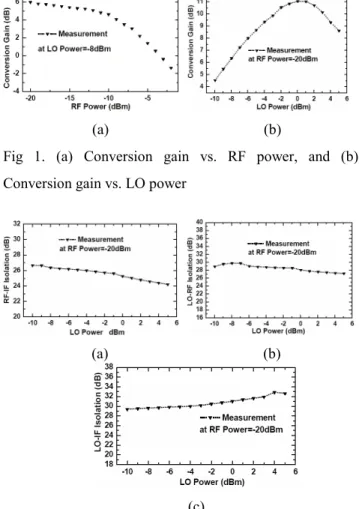
The research in the third year is to accomplish the Mixer and the VCO for the WLAN IEEE 802.11a application. For the design of Mixer, the RF frequency, LO frequency and IF frequency are 5.2 GHz, 5.19 Ghz, and 10MHz, respectively. The Mixer topology is based on the Gilbert cell Mixer. It needs to add a extra-circuit, Balun, to the terminals of the LO and the RF, to make the 180 degree phase difference between these two ports. The measured results are shown as below, and the performance is summarized in the table I.
(a) (b)
Fig 1. (a) Conversion gain vs. RF power, and (b) Conversion gain vs. LO power
(a) (b)
(c)
Fig 2. Isolations of (a) RF-IF, (b) LO-RF, and (c) LO-If
Table I Performance Summary of the Mixer RF Frequency (GHz) 5.2 LO Frequency (GHz) 5.19 IF Frequency (MHz) 10 Vdd (V) 3 DC Current (mA) 8 LO Power (dBm) -8 Conversion Gain (dB) 6 LO-RF Isolation (dB) 29.9 LO-IF Isolation (dB) 29.6 RF-IF Isolation (dB) 26.3 IIP3 (dBm) -2
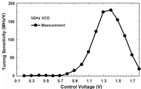
Moreover, a voltage-controlled oscillator (VCO) for the WLAN IEEE 802.11a application was also accomplished in this work. The RF frequency is from 5.725GHz to 5.825GHz.With the desired IF at 480 MHz, the output frequency of VCO should cover 5.265GHz ~ 5.325GHz. This VCO is based on the LC tank topology. The theorem of this LC tank VCO is using transistors cross-coupled pair to produce the positive feedback. When the input resistance of the cross-coupled pair is small or equal to the equalized parallel-resistance of the oscillation port, it will be oscillated, and the oscillation frequency can vary with the value of the varactor. The measurement is performed by using a FR-4 PCB test fixture, and the measured results are shown as below, and the performance is summarized in the table II.
Fig 4. Turning-sensitivity vs. control voltage
Fig 5. Output Power vs. control voltage
Table II Performance Summary of the VCO Control Voltage (V) 0 ~ 1.8
Bias Current (mA) 4 Tuning-range (MHz) 5200 ~ 5440 Tuning Sensitivity (MHz /V) 0 ~ 180
Output Power (dBm) 2.4
四、結論與討論
In this project, we use the SiGe BiCMOS process to accomplish and realize the design of the PA, LNA, Mixer, and VCO. For low noise amplifiers (LNAs), the geometrical scaling issues are used to shift simultaneously the optimum noise and optimum source impedance to a point which is close to 50 Ω. Based on experimental results, optimum device size, layout of low noise cell, and bias suitable for LNAs are determined. In addition, a novel SiGe HBT power cell for the PA application is proposed. It is demonstrated that this novel power cell is superior to
other power cells for the design of the PA. A highly linear SiGe PA for IEEE 802.11a Wireless LAN applications has been demonstrated by adopting a new integrated on-chip linearizer. Furthermore, a high integrated 5.2 GHz inductively degenerated cascode low noise amplifier (LNA) also has been realized in this project. Moreover, a Mixer and a VCO (voltage-controlled oscillator) for IEEE 802.11a Wireless LAN applications are also demonstrated in this work.
本研究群的相關研究結果,於 IEEE 期刊總共發 表 兩 篇 論 文[1]-[2] , 而 在 相 關 會 議 論 文 也 有 三 篇 [3]-[5],並有兩篇期刊論文已經投稿中。
五、參考文獻
1. C.-H. Lin, Y.-K. Su, Y.-Z. Juang, R. W. Chuang, S.-J. Chang, J. F. Chen, and C.-H. Tu, “The Effect of Geometry on the Noise Characterization of SiGe HBTs and Optimized Device Sizes for the Design of Low-Noise Amplifiers,” IEEE Trans. Microwave Theory Tech., vol. 52, no. 9, pp. 2153 - 2162 , Sept. 2004.
2. C.-H. Lin, Y.-K. Su, Y.-Z. Juang, C.-F. Chiu, S.-J. Chang, J. F. Chen, and C.-H. Tu, “The Optimized Geometry of the SiGe HBT Power Cell for 802.11a WLAN Applications,”hasbeen accepted by theIEEE Microwave and Wireless Components Letters.
3. C.-H. Lin, Y.-K. Su, Y.-Z. Juang, and L.-P. Chen, “The Effects of Geometry and Bias Current on the Noise Performance of SiGe HBTs,” International Electron Devices and Materials Symposium, Dec. 20-21, Taipei, Taiwan, 2002.
4. C.-H. Lin, Y.-K. Su, and Y.-Z.Juang,“LinearMMIC SiGe Power Amplifier for 5 GHz WLAN Applications,” Proceeding of the 14th VLSI Design/CAD Symposium, Aug. 12-15, Taiwan, 2003. 5. C.-H. Lin, Y.-K. Su, Y.-Z. Juang, C.-F. Chiu, C.-H. Tu,
S.-J. Chang, and J. F. Chen, “The Optimized Geometry of the SiGe HBT Power Cell for Wireless LAN application at 5 GHz,” International Electron Devices and Materials Symposium, Dec. 20-23, Hsinchu, Taiwan, 2004.