國 立 交 通 大 學
電子工程學系 電子研究所碩士班
碩 士 論 文
鍺對奈米線 pH-靈敏度的影響
The influence of Germanium on the
pH-sensitivity of the nanowire
研 究 生 : 梁家榮
指導教授 : 張 國 明 博士
桂 正 楣 博士
鍺對奈米線 pH-靈敏度的影響
The influence of Germanium on the
pH-sensitivity of the nanowire
研 究 生:梁家榮 Student:Chia-Jung Liang 指導教授:張國明 博士 Advisor:Dr. Kow-Ming Chang 桂正楣 博士 Dr. Cheng-May Kwei
國 立 交 通 大 學
電子工程學系 電子研究所碩士班
碩 士 論 文
A ThesisSubmitted to Institute of Electronics
College of Electrical Engineering and Computer Science National Chiao Tung University
In Partial Fulfillment of the Requirements for the Degree of
Master In
Electronics Engineering
June 2007
Hsinchu, Taiwan, Republic of China
鍺對奈米線 pH-靈敏度的影響
研究生:梁家榮 指導教授:張國明 博士 指導教授:桂正楣 博士 國立交通大學 電子工程學系 電子研究所碩士班摘
要
近年來,由於元件的微縮,使得奈米線和奈米結構變得相當的熱門。 奈米線主要被拿來應用於生物感測器或奈米電子元件,因和傳統元件相 比,其具有較快速的元件轉換速度和低功率消耗之優點。奈米線的側壁相 當的敏感,可用來偵測相當細微的變化。 在這篇研究中,我們引入了矽鍺的應用,來製作出矽鍺奈米線,利用 鍺有比較高的遷移率,故將其以不同比例的鍺摻入矽中,而所成長出的矽 鍺層,會隨著鍺的濃度增加,使我們的元件具有較高的靈敏度。首先我們 將製作好的奈米線滴上 APTES 做表面處理,接著滴上我們要測量的 pH 液。 藉由分析 pH5、pH9、pH11 的改變量我們可以發現奈米線的靈敏度隨著鍺 濃度的增加而增加。但在更高濃度 40%鍺時,其靈敏度低於 30%鍺。我們 猜測可能的原因為太高濃度的鍺會造成更多的表面缺陷。The influence of Germanium on the
pH-sensitivity of the nanowire
Student:Chia-Jung Liang A d v i s o r : K o w - M i n g C h a n g
Cheng-May Kwei
Department of Electronics Engineering & Institute of Electronics National Chiao Tung University
ABSTRACT
Due to the scaling down of devices, nanowire and nanostructure attracts many interests recently. Nanowire is mainly used in biological sensor or nanoelectronics, because it has the advantages of faster switching speeds and lower power consumption than conventional devices. The sidewall of nanowire is very sensitive and this could be used to detect the slight variation of the condition.
In this thesis, we have successfully fabricated the N-SiGe and P-SiGe nanowire with different Ge concentration respectively. The 3-aminopropy- ltriethoxysilane (APTES) was used to modify the surface, which can detect the charge with different pH solution. The percentage change of conductivity among pH5, pH9 and pH11 is calculated to confirm the improvement of SiGe nanowire with different Ge concentration. But our experiment found the higher Ge concentration (40%) has not increased the sensitivity; the reason maybe the higher defect appears at the surface as higher Ge concentration.
誌 謝
首先,我要感謝指導教授張國明老師及桂正楣老師,老師們認真的教 學精神和開明的教學態度,使我這兩年研究生涯獲益匪淺,並讓我能在自 由且輕鬆的環境下致力於研究,在此致上最深的謝意。 謝謝郭俊銘學長在碩士班兩年間給予我的建議及協助,使我的實驗能 順利完成。也感謝趙文全同學,有了他的幫忙與砥礪,使得研究過程不再 單調乏味。也要謝謝 632 實驗室的其他眾多學長們,有了他們的協助,使 得研究能夠更加完整。 謝謝交大奈米中心、國家奈米實驗室提供各種機台設備,讓我可以進 行實驗。 最後,更感謝我的父母,梁炳明先生與林瑞霞女士,感謝他們對我從 小到大的養育及栽培,在生活上給我無微不至的關心,並在我情緒低落時 帶給我溫暖及鼓勵,讓我得以全心完成學業。我相信他們會以我為榮。Contents Chinese Abstract………i English Abstract………...ii Acknowledgement………...iii Contents………...iv Figure Captions………..……….…vi Table Captions………...……..……..viii Chapter 1 Introduction……….... 1
1.1 The introduction of nanowires……….1
1.2 The ways to fabricate nanowires………..2
1.2.1 Lithography with photons………3
1.2.2 Machining using AFM, STM, NSOM……….3
1.2.3 nano imprinting……….…………..4
1.2.4 Self- assembly by using surfactant systems………4
1.2.5 Spacer formation……….5
1.2.6 Laser Ablation………5
1.2.7 Solid-Liquid-Solid………..5
1.3 The application of nanowires………..6
1.3.2 The application of metal nanowires………...…….…8
1.3.3 The application of metal-oxide nanowires……….………...8
1.3.4 The application of semiconductor nanowires………...10
Chapter 2 Experiment… ……..………...15
2.1 Device fabrication……….……...……..15
2.2 Detail fabrication process………..….……...15
2.3 Test structure………...………...17
2.4 The process of measurement……….……….17
Chapter 3 Results and Discussions……….…..….…19
3.1 SiGe Nanowire Fabrication……….……..…....19
3.2 Cross-Section View of SEM………..…………...……19
3.3 Make the nanowire Comparison of N-type and P-type………...….20
3.4 The same concentration of Ge is compared with different PH solution….…..20
3.5 The comparison of conductance and conductivity with different pH solution………...…..……...21
3.6 The influence of Ge on the sensitivity of the nanowire……….…....…21
Chapter 4 Conclusion………...……….……….24
Chapter 5 Future Work……….….……25
Figure Captions
Fig. 1-1 Schema of Scanning Probe Lithography (SPL). Fig. 1-2 Schematic process flow of nanoimprint.
Fig. 1-3 Binary Phase Diagram for the Au:Ge and SEM image of Ge nanowires Synthesized.
Fig. 1-4 Schematic view of iterative spacer lithography (ISL). Fig. 1-5 The mechanisms of the laser ablation formation technique. Fig. 1-6 VLS mechanism and SLS mechanism.
Fig. 1-7 Fabrication of a stretched double-stranded DNA polyaniline nanowire. Fig. 1-8 Detection of the HCl and the NH3.
Fig. 1-9 Detection of the hydrogen.
Fig. 1-10 Detection of the NO2 and the NH3.
Fig. 1-11 ZnO nanowire reducing sensing to NH3 at 500 K.
Fig. 1-12 The response of nanowire conductance to 0.5% CO in 20% O2 at 500 K.
Fig. 1-13 NW nanosensor for pH detection. Fig. 1-14 Real-time detection of protein binding.
Fig. 1-15 Real-time detection of reversible protein binding. Fig. 1-16 Real-time detection of Ca2+ ions.
Fig. 1-17 Real-time detection of DNA. Fig. 2-1 The thickness of the oxide is 5000Å.
Fig. 2-2 Mask #01 dry etching 3000 Å from oxide Step. Fig. 2-3 Deposited amorphous Si film.
Fig. 2-5 Define the S/D of SiGe nanowire.
Fig. 2-6 Remove one side of the parallel SiGe spacer. Fig. 2-7 After thermal coating Al for 5000 Å.
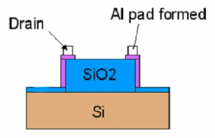
Fig. 2-8 Defined the Al contact pad in the Mask #04. And then sintering at T=420℃ for 25 min.
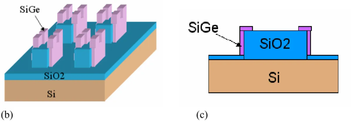
Fig. 2-9 The schematics of the two SiGe block film. Fig. 2-10 The test structure of each block.
Fig. 3-1 The Cross-Section view of the SEM of Si0.93Ge0.07 nanowire, the Si0.93Ge0.07 nanowire
is 77.7 nm in width and 192 nm in height.
Fig. 3-2 The Cross-Section view of the SEM of Si0.89Ge0.11 nanowire,the Si0.89Ge0.11 nanowire
is 45.4 nm in width and 184 nm in height.
Fig. 3-3 The Cross-Section view of the SEM of Si0.8Ge0.2 nanowire,the Si0.8Ge0.2 nanowire is
65.9 nm in width and 159 nm in height.
Fig. 3-4 The Cross-Section view of the SEM of Si0.7Ge0.3 nanowire,the Si0.7Ge0.3 nanowire is
54.5 nm in width and 153 nm in height.
Fig. 3-5 The Cross-Section view of the SEM of Si0.6Ge0.4 nanowire,the Si0.6Ge0.4 nanowire is
53.4 nm in width and 172 nm in height.
Fig. 3-6 The ID-VD of the Si0.93Ge0.07 nanowire of P-type with the length L=5μm.
Fig. 3-7 The ID-VD of the Si0.89Ge0.11 nanowire of P-type with the length L=8μm.
Fig. 3-8 The ID-VD of the Si0.8Ge0.2 nanowire of P-type with the length L=9μm.
Fig. 3-9 The ID-VD of the Si0.7Ge0.3 nanowire of P-type with the length L=6μm.
Fig. 3-10 The ID-VD of the Si0.93Ge0.07 nanowire of N-type with the length L=5μm.
Fig. 3-11 The ID-VD of the Si0.89Ge0.11 nanowire of N-type with the length L=8μm.
Fig. 3-12 The ID-VD of the Si0.8Ge0.2 nanowire of N-type with the length L=9μm.
Fig. 3-13 The ID-VD of the Si0.7Ge0.3 nanowire of N-type with the length L=6μm.
Fig. 3-15 The ID-VD of the Si0.89Ge0.11 nanowire of P-type with the length L=5μm.
Fig. 3-16 The ID-VD of the Si0.8Ge0.2 nanowire of P-type with the length L=10μm.
Fig. 3-17 The ID-VD of the Si0.7Ge0.3 nanowire of P-type with the length L=6μm.
Fig. 3-18 The ID-VD of the Si0.6Ge0.4 nanowire of P-type with the length L=7μm.
Fig. 3-19 The ID-VD of the N-type Si0.93Ge0.07 nanowire with the length L=11μm.
Fig. 3-20 The ID-VD of the N-type Si0.89Ge0.11 nanowire with the length L= 6μm
Fig. 3-21 The ID-VD of the N-type Si0.8Ge0.2 nanowire with the length L= 50μm.
Fig. 3-22 The ID-VD of the N-type Si0.7Ge0.3 nanowire with the length L= 15μm.
Fig. 3-23 The conductance of the Si0.93Ge0.07 nanowire changes with the various PH solution.
Fig. 3-24 The P-type conductance of the Si0.89Ge0.11 nanowire changes with the various pH
solution.
Fig. 3-25 The P-type conductance of the Si0.8Ge0.2 nanowire changes with the various pH
solution.
Fig. 3-26 The P-type conductance of the Si0.7Ge0.3 nanowire changes with the various pH
solution.
Fig. 3-27 The P-type conductance of the Si0.6Ge0.4 nanowire changes with the various pH
solution.
Fig. 3-28 The N-type conductance of the Si0.93Ge0.07 nanowire changes with the various pH
solution.
Fig. 3-29 The N-type conductance of the Si0.89Ge0.11 nanowire changes with the various pH
solution.
Fig. 3-30 The N-type conductance of the Si0.8Ge0.2 nanowire changes with the various pH
solution.
Fig. 3-31 The N-type conductance of the Si0.7Ge0.3 nanowire changes with the various pH
Fig. 3-32 The P-type sensitivity is improves with the increase concentration of Ge at low concentration of Ge. [percentage % = (pH9-pH5)/pH5]
Fig. 3-33 The N-type sensitivity is improves with the increase concentration of Ge. [percentage % = (pH9-pH5)/pH5]
Fig. 3-34 The P-type sensitivity is improves with the increase concentration of Ge. [percentage % = (pH11-pH5)/pH5]
Fig. 3-35 The N-type sensitivity is improves with the increase concentration of Ge. [percentage % = (pH11-pH5)/pH5]
Table Captions
Table 1………..43 Table 2………..57
Chapter 1
Introduction
1.1 The introduction of nanowires
Semiconductor nanowires (NWs) are nowadays intensively studied due to their great potential for nanoscale electronic and photonic devices [1~2]. Single NW resonant tunneling diodes [3], photodetectors [4], as well as light emitting diodes [5] and lasers [6] have recently been demonstrated.
Semiconductor 1D nanostructures such as carbon nanotubes, III-V, II-VI, Si-Ge, and metal-oxide have been synthesized and studied for their nanoscale properties.Their reduced dimensionality leads to higher quality, defect-free material with high surface-to-volume ratio[7].The latter is now utilized in the construction of gas sensing devices when the surface properties are modified by adsorption of chemical gas or liquid[39~43], which in turn affects the electronic properties of the wire.When the size of the nanowire is smaller than the exciton’s Bohr radius in the bulk, the electronic properties are defined by the size due to quantum confinement effects.
In fact, the downscaling of material dimension does not only imply an increase in device packing density and a decrease in power consumption, but also it renders superior sensitivity to surface adsorption related chemical processes. As it has been reported, chemical sensing with nanowires and nanotubes is usually realized by monitoring their conductance change upon exposure to the target chemicals [8~10]. Compared with their bulk and thin-film counterparts,in addition to a larger surface-to-volume ratio, the 1D structure has radius comparable to the Debye screening length, so that chemisorption induced surface states effectively alter the electronic property of the nanowire, yielding
enhanced sensitivity.
1.2 The ways to fabricate nanowires
One-dimensional nanostructures, such as nanotubes, nanowires, nanorods, and nanobelts, are receiving increasing attention because finite size effects result in various unusual properties enabling novel electronic, optical, and mechanical nanodevices[11~12]. Nanowires of different compositions have been prepared by a variety of methods including laser ablation[13], template-assisted electrochemistry[14~15], chemical transportation[16], chemical vapor deposition[17~18] and solvothermal methods[19], and semiconductor-based nanostructures are of increasing interest. Although there are many reports considering silicon nanowires [20~21], only a few publications concerning the preparation of germanium nanowires existed until now [22~25].
Silicon nanowires are important because they are totally compatible with Si-based microelectronics. Since the discovery of Si whiskers [26], silicon nanowires (SiNWs) have attracted much attention in mesoscopic research and device applications as well as in fundamental research because of their highly interesting optical and electrical properties. Several fabricate methods, including are (1) lithography with photons in UV, DUV, EUV and X-ray spectrum; (2) machining using AFM, STM, NSOM; (3) replication against masters (or molds) via physical contact printing, molding and embossing; (4) self- assembly by using surfactant systems, block copolymers, crystallization of proteins and colloids; (5) spacer formation; (6)Vapor-Liquid-Solid; (7) Laser Ablation .
1.2.1 Lithography with photons
In photon and particle-based lithography, by using nonlinear resists, near-field phase shifting or topographically directed technology, it has been possible to achieve sub-50nm feature. For example, EBL has demonstrated the ability to achieve 20nm width nanowires with 60nm height. Height is often limited by the lift-off process. Extreme ultraviolet light (EUV) lithography has generated 38nm patterns [27].
1.2.2 Machining using AFM, STM, NSOM
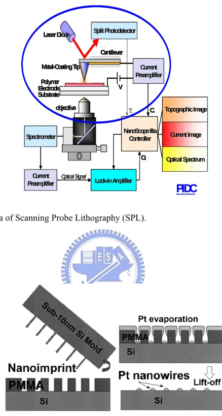
In 1990, J. A . Dagata et al. proposed the tip-induced anodic surface oxidation by using scanning probe lithography (SPL) (Fig. 1-1) to define nano- patterns on the semiconductor surface. AFM, STM, NSOM and the like are called SPM. Its operation mechanism is in an environment humidity control when approximately 50%, the sample surface attaches a water thin film, when the probe contacts this water thin film, take the probe as negative electrode, the sample surface is the positive electrode, gives a negative bias to probe, the water molecule can start to ionization, and produces the partial region oxide compound with the probe underneath sample surface. The probe produces the electric field can along with the distance of sample surface to attenuation, the oxidation stops
immediately when the electric-field intensity is smaller than 109 V/m [28]. The
oxide compound growth speed with executes gives the probe bias to have the enormous relations. In process by way of program configure, but fine holds controls scans the probe the displacement, carries on oxide compound of the specific line to grow, then achieves the micro region design forming the goal, this is scanning probe lithography technique to apply to the lithography at the beginning of shape.
1.2.3 nano imprinting
In microcontact printing, micromolding [29], embossing and nano-imprinting techniques (Fig. 1-2) [30], issues limited by van der Waals forces , speed of capillary filling and adhesion of mold and replica are overcome by using low-viscosity solutions and surface modification. Step and flash technology has demonstrated the ability to imprint sub-20nm features [31]. Although such methods may translate the serial method of EBL/EUV into a parallel patterning process, the mold formation still depends on EBL/EUV and it’s use restricted by the high cost of molds.
1.2.4 Self- assembly by using surfactant systems
Germanium is an important semiconducting electronic material with high carrier mobility and a band gap of approximately 0.6 eV. Those high quality Ge
nanowires are synthesized by a simple CVD process at 275 under atmospheric ℃
pressure. This represents the mildest growth conditions for single-crystal
nanowire synthesis. An efficient Ge feedstock from GeH4 and the low eutectic
temperature of Ge-Au nanoclusters are the key factors that afford vapor-liquid-solid (VLS) growth of Ge nanowires at low temperatures (Fig. 1-3).
Dunwei Wang et al. carried out CVD growth at 275 under a 10 sccm ℃
(standard cubic centimeter) flow of GeH4 (10% in He) in tandem with a 100
sccm flow of H2 in a 2.5 cm furnace reactor (total gas pressure 1 atm) for 15 min.
The SiO2 substrate used in this work contained preformed Au nano- crystals (approximately 20 nm in diameter) deposited uniformly on the surface from a colloidal solution.
1.2.5 Spacer formation
Controlled deposition and size reduction, which involves deposition on cleaved edges, or oxidation, followed by anisotropic etching forming spacers (Fig. 1-4). This process provides a density increase as well as size reduction. It can be used to pattern silicon fins for double-gate MOSFETs [32].
1.2.6 Laser Ablation
A method combining laser ablation cluster formation and VLS growth was developed for the synthesis of semiconductor nanowires [33]. In this process, laser ablation was used to prepare nanometer diameter catalyst clusters that define the size of wires produced by VLS growth. This approach was used to prepare bulk quantities of uniform single-crystal Si and Ge nanowires with diameters of 6 to 20 and 3 to 9 nm, respectively, and lengths ranging from 1 to 30 micrometers. The schematics are shown in Fig. 1-5. In the Laser ablation technique, (1) Laser ablation with photons of energy hν of the SiFe target creates a dense, hot vapor of Si and Fe species. (2) The hot vapor condenses into small clusters as the Si and Fe species cool through collisions with the buffer gas. The furnace temperature is controlled to maintain the Si-Fe nanocluster in a liquid state. (3) Nanowire growth begins after the liquid becomes supersaturated in Si and continues as long as the Si-Fe nanoclusters remain in a liquid state and Si reactant is available. (d) Growth terminates when the nanowire passes out of the hot reaction zone onto the cold finger and the Si-Fe nanoclusters solidify.
1.2.7 Solid-Liquid-Solid
element phosphides and arsenides, which are thermally stable at conventional growth temperatures. However, indium nitride is not. The SSLS mechanism operates at very low temperatures in comparison to conventional materials-synthesis methods, presumably because it is catalytic and lowers energy barriers for both precursor decomposition and the interfacial steps required for nonmolecular crystal growth. The crystal lattice is assemble. SLS synthesis of other thermally unstable compounds and crystal structures should be possible [34~36]. The VLS and SLS grown mechanisms was explained in Fig. 1-6.
1.3 The application of nanowires
Nanowires have emerged as promising elements for chemical and biological sensing, with proof-of-principle devices demonstrated for detection of various gases [37~39], pH in aqueous media [40], antibody binding [40], calcium ions[40], DNA hybridization[41] and Hydrogen [42] .The high surface-to-volume ratio of nanowires results in a strong dependence of carrier concentration on charge transfer from the surface and changes in nanowire conductance. Silicon nanowires (SiNWs) are particularly appealing for sensing applications, since the Si oxide can effectively passivate surface dangling bonds, and at the same time can be chemically modified through the well known silanol chemistry to provide surface functionalization and selectivity for particular analytes.
Nanowires, such as semiconductor, metal and conducting polymer and metal-oxide nanowire have been the subject of intense interest as sensors.
1.3.1
The application of polymer
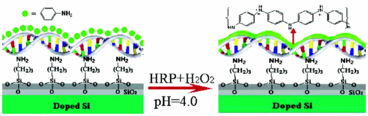
nanowiresConducting polymer nanowires were obtained primarily with porous membrane as templates. In this approach,the dimension and the morphology of the polymer structures are defined by the porous support. Polyaniline nanowires with 3-nm diameter and polypyrrole nanowires of 30-nm diameter have been successfully fabricated by this method [43~44]. The principle of the nanowire fabrication method is sketched in Fig. 1-7. First, double-stranded λ-DNA is stretched, aligned, and immobilized on a thermally oxidized Si chip by the molecular combing method [45~46]. Then the DNA templates are incubated in protonated aniline monomer solution to emulsify and organize the aniline monomers along the DNA chains. Finally, the aligned aniline monomers are
polymerized enzymatically by adding horseradish peroxidase (HRP) and H2O2
successively to form polyaniline/DNA nanowires.
DNA Alignment. The thermally oxidized Si substrate was modified with
(aminopropyl)triethoxysilane (APTES)[47]; a vapor-phase method was used to provide a good adhesion between DNA strands and the substrate surface. A 2 µL drop of λ-DNA (48 500 bp, New England Biolabs Inc.) solution in TE buffer (10 mM Tris-HCl and 1 mM EDTA, pH = 8.0) was deposited onto the edge of a clean glass coverslip, and carefully placed onto the top of the APTES-modified Si surface. The weight of the glass forced the solution to spread into a thin layer. When the cover glass was slid away, the capillary force of the moving interface stretched and aligned the DNA in one direction.
Conductance of the Polymer Nanowires. To measure the conductivity of the
polyaniline nanowires, we first immobilized the DNA strands across an array of interdigitated gold electrodes with gaps of about 1.5 µm. The array consists of
10 pairs of electrodes on a silicon substrate with a thermal oxide layer. When the wires were exposed to HCl vapor, a large current increase was observed [Fig.
1-8(a)] , then No current increase was observed when NH3 gas was introduced
since the water-cleaned polyaniline nanowires had been undoped before the
measurements. Introducing NH3 gas in previously HCl-doped polyaniline
nanowires caused a decrease of the conductance to almost zero [Fig. 1-8(b)] (the initial increase and then decrease of the conductance was caused by mechanical
interference when the NH3 gas was introduced into the chamber). The
conductance drop can be attributed to the deprotonation of polyaniline by the
NH3 gas. This typical proton doping-undoping phenomenon further confirmed
the formation of polyaniline nanowire arrays and also demonstrated the potential for sensitive gas-sensing applications of the nanowires.
1.3.2
The application of metal
nanowiresFor Hydrogen sensor, using a single electrodeposited Pd wire (Fig. 1-9) with 100 nm diameter and 4 µm length, sensing of different concentrations of
hydrogen gas (between 0.02% and 10% in N2 gas) has been demonstrated [48].
Additionally, that has simulated hydrogen sensor using nanowire for the depth understanding of the H/Pd material system.
1.3.3
The application of metal-oxide
nanowiresWe report chemical sensing studies with zinc oxide (ZnO) nanowires configured as FETs. It is noteworthy that this device configuration can not only facilitate the monitoring of conductance change, but also utilize a transverse electric field to modulate the chemical sensing behavior of the nanowires,since
the external field regulates the surface chemisorption activity [49]. Various
gases have been used in the chemical sensing study,such as O2 , NO2 , NH3 , and
CO. The monitoring of these gases in the environment is of paramount importance. As is known,chemisorbed gas molecules on a metal–oxide surface withdraw or donate electrons to the conduction channel, giving rise to a conductance change. Experiments have demonstrated that ZnO nanowire
exposure to O2 , NO2 and NH3 at room temperature show decreased conductance.
As shown in Fig. 1-10(a), nanowire conductance decreased when it was exposed
to different concentrations of NO2 varying from 1 to 20 ppm, and the sensing
response increases with under higher concentration. Fig. 1-10(b) plots the
time-domain response of the nanowire conductance to 1% NH3 at room
temperature. In this case, a refresh process is also demonstrated. As reported in [38], a large negative gate field assists the surface desorption process, and thus leads to a fast recovery of nanowire conductance. As shown in Fig. 1-10(a) and
(b), 2-ppm NO2 causes 50% conductance decrease while 1% NH3 yields the
same effect. This difference is due to the higher binding strength between NO2
molecules and the nanowire surface. Interestingly, it was observed that NH3
sensing at 500 K has the opposite effect compared to that at room temperature,
i.e., the ZnO nanowire conductance increased upon exposure to NH3 at 500 K,
as illustrated in Fig. 1-11, indicating that the chemisorbed NH3 molecules donate
electrons to ZnO nanowire. Oxidizing and reducing sensing of NH3with In2O3
nanowires at room temperature has been reported and attributed to a doping dependent Fermi level shift [50].
As observed in our experiment, under the same concentration of NH3 gas
(1%), the relative conductance change is considerably smaller at 500 K (Fig. 1-11) as compared to that at room temperature [Fig. 1-10(b)].In addition to the
sensing response to O2 , NO2 and NH3 ,we have also investigated the response of
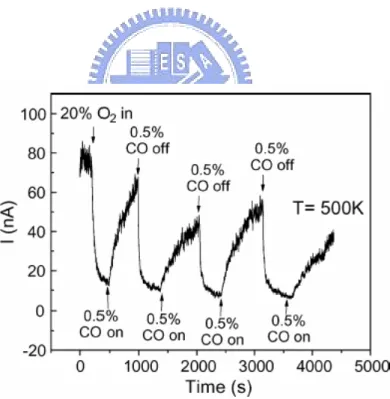
ZnO nanowires to CO gas in the presence of O2 . It is observed that the nanowire
conductance is increased at 500 K. Fig. 1-12 demonstrates the time-domain measurement of nanowire conductance when the nanowire is exposed to 0.5%
CO in 20% O2 at 500 K. It can be seen that nanowire conductance first decreases
upon admittance of 20% O2 ; however, the subsequent admittance of CO
increases the nanowire conductance. It is known that CO is a combustible gas;the sensing of CO is based on the reaction between CO and the preadsorbed
oxygen species to form CO2 [51].
1.3.4
The application of
semiconductor nanowiresTo explore pH sensors. The underlying concept of our experiments is
illustrated first for the case of a pH nanosensor [Fig. 1-13(A)]. Here a silicon NW (SiNW) solid state FET, whose conductance is modulated by an applied gate, is transformed into a nanosensor by modifying the silicon oxide surface with 3-aminopropyltriethoxysilane (APTES) to provide a surface that can undergo protonation and deprotonation,where changes in the surface charge can chemically gate the SiNW.The response of the conductance of APTES-modified SiNWs to changes in solution pH was evaluated by fabricating a cell consisting of a micro fluidic channel formed between a poly(dimethylsiloxane)(PDMS) mold [52~ 53] and the SiNW/substrate.We could carry out continuous flow or static experiments and could readily change pH. Measurements of conductance as a function of time and solution pH [Fig. 1-13(B)] demonstrate that the NW conductance increases stepwise with discrete changes in pH from 2 to 9 and that
the conductance is constant for a given pH; the changes in conductance are also reversible for increasing and/or decreasing pH. A typical plot of the conductance versus pH [Fig. 1-13(C)] shows that this pH dependence is linear over the pH 2 to 9 range and thus suggests that modified SiNWs could function as nanoscale pH sensors. In addition,It believe the uncertainty in slope of the conductance versus pH obtained from the different SiNW pH sensors studied to date;100 ±20 nS/pH, is quite good and could be improved by placing further effort on controlling reproducibility of the SiNW surface modification.These conductance measurements show a nonlinear pH dependence: The conductance change is small at low pH (2 to 6) but large at high pH range (6 to 9). Notably, these pH measurements on unmodified SiNWs are in excellent agreement with previous measurements of the pH-dependent surface charge density derived from silica [54] [Fig. 1-13(D)].
To explore biomolecular sensors. We functionalized SiNWs with biotin and
studied the well-characterized ligand-receptor binding of biotin-streptavidin [Fig. 1-14(A)][55]. Measurements show that the conductance of biotin-modified SiNWs increases rapidly to a constant value upon addition of a 250 nM streptavidin solution and that this conductance value is maintained after the addition of pure buffer solution [Fig. 1-14(B)].The increase in conductance upon addition of streptavidin is consistent with binding of a negatively charged species to the p-type SiNW surface and the fact that streptavidin (pH= 5 to 6) is negatively charged at the pH of our measurements. The absence of a conductance decrease with addition of pure buffer is also consistent with the
small dissociation constant (Kd ~10-15 M) and correspondingly small
were carried out to confirm that the observed conductance changes are due to the specific binding of streptavidin to the biotin ligand.First, addition of a streptavidin solution to an unmodified SiNW did not produce a change in conductance [Fig. 1-14(C)]. Second, addition of a streptavidin solution in which the biotinbinding sites were blocked by reaction with 4 equivalents of d-biotin produced essentially no change in the conductance of biotin-modified SiNWs [Fig. 1-14(D)]. These controls show that there is little nonspecific binding of the protein to either bare or biotin-modified SiNW surfaces. It also explored the sensitivity limits of biotin-modified SiNWs nanosensors and find that it is possible to detect streptavidin binding down to a concentration of at least 10 pM [Fig. 1-14(E)] . This detection level is substantially lower than the nanomolar range demonstrated recently by stochastic sensing of single molecules [56].
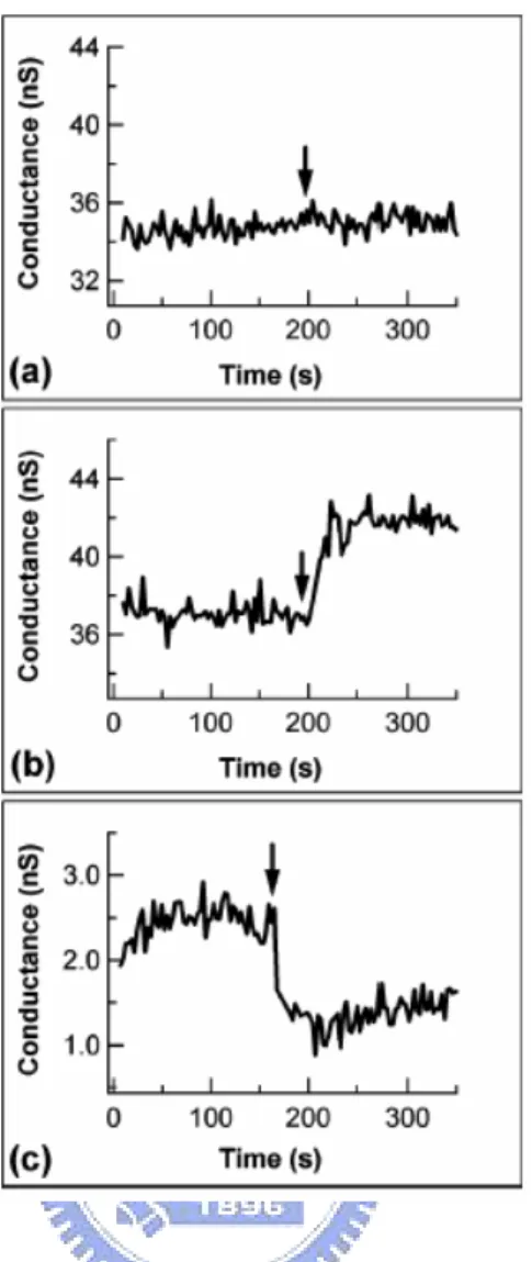
Although the essentially irreversible biotin-streptavidin binding interaction precludes real-time monitoring of vary protein concentrations. To explore this issue, we studied the reversible binding of monoclonal antibiotin (m-antibiotin) with biotin [57].Time-dependent conductance measurements made on biotin-modified SiNWs [Fig. 1-15(A)]exhibit a well-defined drop after addition of m-antibiotin solution followed by an increase in the conductance to about the original value upon addition of pure buffer solution. Control experiments demonstrate that the observed results are due to specific antibody binding to the surface antigen. First, unmodified SiNWs do not exhibit a conductance change after adding m-antibiotin [Fig. 1-15(B)]. Second, addition of immunoglobulin G (IgG), which is not specific for biotin, does not result in a change in conductance,whereas subsequent addition of m-antibiotin solution produces a conductance drop, as observed in Fig. 1-15(C).We extended these reversible, real-time antibody detection experiments by monitoring the SiNW sensor
conductance as a function of m-antibiotin concentration. We observed a linear change in the conductance as a function of m-antibiotin concentration below ~10 nM and saturation at higher values [Fig. 1-15(D)].
To explore calcium ions sensors. We investigated sensing of calcium ions
(Ca2+), which are important for activating biological processes such as muscle
contraction, protein secretion, cell death, and development [58]. We created a
Ca2+ sensor by immobilizing calmodulin onto SiNW surfaces. Data recorded
from modified SiNW devices [Fig. 1-16(A)] showed a drop in the conductance
upon addition of a 25 µM Ca2+ solution and a subsequent increase when a
Ca2+-free buffer was subsequently flowed through the device. Control
experiments carried out with unmodified SiNWs [Fig. 1-16(B)] did not exhibit a
conductance change when Ca2+ is added and thus demonstrate that the
calmodulin receptor is essential for detection. In addition, the observed conductance decrease in modified SiNWs is consistent with expected chemical
gating by positive Ca2+, and the estimated dissociation constant, 10-5 to 10-6 M,
is consistent with the reported Kd for calmodulin [58].For the sensitized SiNWs,
sequence-specific DNA detection was achieved by monitoring the conductance of the SiNWs, while the target DNA solution was injected into a purpose-built sensor chip testing apparatus. We used only high purity water (>18 MΩ, Nanopure, Barnstead, IA) as the solvent in this study because the charge-based detection is most sensitive when counterion screening of the negatively charged DNA molecules is minimized. Fig. 1-17 shows the conductance traces of two representative SiNWs: (a, b) a boron-doped, p-type wire with nominal doping
density of 1019 cm-3, and (c) a phosphorus-doped, n-type sample with nominal
doping density of 1018 cm-3. Control experiments with noncomplementary DNA
above the noise level [as shown in Fig. 1-17(a)]. On the other hand, the real-time increase of the conductance of the p-type SiNW upon the addition of complementary ss-DNA was observed [as shown in Fig. 1-17(b)]. A similar change of the magnitude of the conductance was observed in n-type samples,but in the opposite direction [Fig. 1-17(c)]. When the target DNA attached to its complementary DNA on the SiNW surfaces, the increase of negative charges introduced by the DNA enhanced (or reduced) the carrier concentrations in the p-type (or n-type) SiNWs, resulting in the observed changes of the SiNW conductance. The responses of the sensors for p-type and n-type nanowires were 12% and 46%, respectively, and signal/noise ratios were 8 and 6, respectively.
[Response is defined as (IDNA-I0)/I0, and S/N ratio is calculated by dividing the
Chapter 2
Experiment
2.1 Device fabrication
An easy process to fabricate a nanostructure with high-yield and low-cost is the main issue to be concerned. The fabrication only using the combination of the conventional lithography and process technology was demonstrated without using EBL, SPL, VLS, etc. in the thesis. Nanowire would be formed by dry etching the film. Our process involves defining the active area (AA) by etching an island by conventional G-line lithography, followed by deposition of SiGe layer. Later, the conformal SiGe layer is etching back to the edge of the island by dry etching. The thickness of the island determines the height and width of the nanowires.
2.2 Detail fabrication process
A p-type (100)-oriented bare silicon wafer was prepared. The resistivity of the silicon substrate is about 1~10Ω-cm.
1. Zero layer formation – Zero mask dry etch to form the alignment mark. 2. Standard RCA cleaning, 980℃Wet Oxidation for ~6 hr to grow the bottom
oxide as a gate oxide by ASM/LB45 Furnace system. The thickness of the oxide is 5000Å. It was shown in Fig. 2-1
3. Mask #01: Define the AA region. The oxide film was etched to form each step by TEL oxide etcher – TEL 5000. It was shown in Fig. 2-2. In mask #01,
the residue thickness of the oxide is around 2000~2300Å and this should be precisely controlled (In Fig.2-2). If the oxide left too thick, the control ability of the oxide would become weak. The Surface Profiler was used to check whether if the step is the height we want or not. We controlled the height is about 2000 Å.
4. Standard RCA cleaning. Before the deposition of SiGe film, we deposited amorphous Si film first by ASM/LB45 Furnace system. It was shown in Fig.
2-3. This purpose is due to the bad adhesion between SiGe and SiO2. The
growth condition of the amorphous Si was 650℃ for 2 hours and the pressure was controlled at 389 mTorr, and it’s thickness was 150 Å.
5. We treated the wafers for standard RCA cleaning again after the amorphous Si deposition because of the better uniformity compared to the without cleaning one. The SiGe film deposited with the ultra-high-vaccum chemical vapor deposition (ANELAVA SiGe UHV-CVD). The structure was shown in Fig. 2-4. The condition of the SiGe film was epitaxially grown at 665℃. After deposition, we measured the testing wafer by N&K Analyzer 1280 to confirm the SiGe thickness and how much the thickness should we etch. The SiGe thickness was varies with different concentration.
6. Mask #02: Defined the S/D region. Etching the whole height of the amorphous Si and SiGe film by TCP poly etcher – TCP 9400 SE. Only the S/D and SiGe deposited in the sidewall spacer will be stayed. And the residue SiGe film is what we want – SiGe nanowire. The structure is shown in Fig. 2-5. The height of the oxide step was measured by Scanning Electron
Microscopy (SEM).
parallel SiGe nanowire by TCP poly etcher – TCP 9400 SE. It prevents parallel SiGe nanowire from shorting out each other. The structure is shown in Fig. 2-6.
8. The condition of the ion implantation (p-type or n-type) in our experiments was energy E=15keV and dose D=5E15.
9. After ion implant, we treated the device and then thermal annealing at T=950 ℃ for 30 min for the dopants activation.
10. Thermal coating of the aluminum as contact electrode for the thickness of 5000 Å at 30~40℃. This is shown in Fig. 2-7.
11. Mask #04: Aluminum contact pad were then defined by wet etching
(HNO3:CH3COOH:H3PO4:H2O=2:9:50:10)
12. Sintering at T=420℃ for 25 min. The schematic is shown in Fig. 2-8.
2.3 Test structure
The test structure we designed was used to make sure that the SiGe was etched completely in the isolation area. The test structure is shown in Fig. 2-9. A series test block was used to calculate the contact resistance between the Al electrode and SiGe or Poly-Si film. Fig. 2-10 shows the contact resistance test structure. The two test structure was experimented with the process flow. So the all process condition was the same with the devices.
2.4 The process of measurement
1. Before the measurement, the B and P ion was implanted to form the N-type and P-type SiGe nanowire.
2. The measure condition was set VD = −10V to 10V in 0.2V step and VG = −15
V, 0 V and 15 V respectively.
3. The 3-aminopropy-ltriethoxysilane (APTES) was used to modify the surface, which can detect the charge with different pH.
4. Drip pH 1 solution, and then the surface was dried by nitrogen purge. 5. D.I. Water was utilized to wash the surface after measurement.
Chapter 3
Results & Discussion
3.1 SiGe Nanowire Fabrication
We have successfully fabricated the SiGe nanowire structure on the Si
wafer by spacer technique and measured the electric characteristics. As we known, the diameter of the nanowire would influence the current, so the control of the nanowire would become a key issue. This was controlled by the Mask #02 when we etched the SiGe film by TCP poly etcher – TCP 9400 SE. The surface of the nanowire is quite sensitive so that it’s easy influence by any variances.
3.2 Cross-Section View of SEM
We observed the cross-section view of different concentration nanowire by Scanning Electron Microscopy (SEM). The area of the nanowire could be calculated by the TFSEM. The JOEL JSM 6500-F – TFSEM was the equipment we used to measure the diameter of the nanowires. Fig. 3-1 shows the
cross-section view SEM picture of Si0.93Ge0.07 nanowire. There was fluctuation
in each width and height which was controlled by the TCP dry etcher. The fluctuation must be decreased because the diameter of the nanowire is directly
related to the current. The average of the Si0.93Ge0.07 nanowire is 192 nm in
height and 77.7 nm in width. We thought that the nanowire was a triangle
column shape, so the average area is about 14918.4 nm2. Similarly, Fig. 3-2~3-5
show the cross-section view SEM picture of SiGe nanowires with different Ge concentration. All the data are summarized on the Table 1.
3.3 Make the nanowire Comparison of N-type and P-type
Electrical-transport measurements were conducted using an Agilent 4156C
semiconductor parametric analyzer. We sweep the ID-VD figure from –10V to
10V, and change the VG step from –15, 0V and 15V. Fig. 3-6 show the ID-VD
figure of the Si0.93Ge0.07 nanowire of P-type with the length L=5µm. For
comparison, we fabricated the same nanowire of N-type (Fig. 3-10) and the same way to measured. Similarly, we compared the electronic properties of Fig 3-7 to 3-9 and Fig.3-11 to 3-13. It seems that the current of the N-type nanowire would be larger than that of P-type nanowire.
3.4 The same concentration of Ge with different pH solution
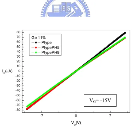
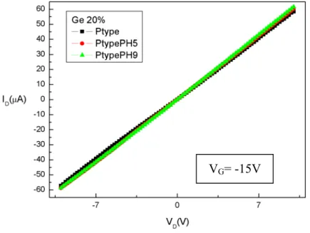
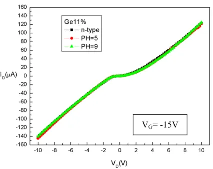
Before the measurement, the P and B ions were implanted to form the N–type and P–type SiGe nanowire, respectively. The 3-aminopropy-ltriethoxysilane (APTES) was used to modify the surface, which
can detect the charge with different pHs. Fig. 3-14 shows the ID-VD curves of
P-type Si0.93Ge0.07 nanowire with pH3, pH5, pH9 and pH11 solutions at VG
= –15V and VD = –10V to 10V. The higher current is obtained for pH11 solution.
Similarly is shown in Fig. 3-15~3-18, current increase with the incensement of pHs under the different concentration of Ge. On the other way, Fig. 3-19 shows
the ID-VD curves of N-type Si0.93Ge0.07 nanowire with pH3, pH5, pH9 and pH11
solutions at VG = –15V and VD = –10V to 10V. The higher current is obtained for
pH3 solution. Similarly is shown in Fig. 3-20~3-22, current decrease with the incensement of pHs under the different concentration of Ge.
3.5 The comparison of conductance and conductivity with
different pH solution
The equation about resistance R is
∆V = ∆I · R = ∆I · ρ (L/A) → (3.1) conductance :(1/R)=( ∆I / ∆V ) → (3.2)
ρ is the resistivity. The (1/R) is the conductance (S).We fix the voltage ∆V at
0.2V to be constant. Using the formula (3.2), conductance of nanowire can be calculated. The average conductance between –4 V to –8 V was obtained. The
conductance of P-type Si0.93Ge0.07 nanowire increases as the enhancement of pH
solution (Fig. 3-23). Fig. 3-24~3-27 show the conductance versus pH in other Ge concentrations, and all the figures show the enhancement in higher pH
solution. Contrasting the P-type nanowire, the trend of conductance with N-type
Si0.93Ge0.07 nanowire become lower as increase of pHs solution (Fig. 3-28). Fig.
3-29~3-31 show the conductance versus pH in other Ge concentrations, and all the figures show the conductance decrease as the pH increase. All the data were summarized on the table 2.
3.6 The influence of Ge on the sensitivity of the nanowire
As we known, there is still some reason will affect the drive current including the diameter of the nanowire, wire length, the dopant condition, heat treatment, and the electrode contact, etc. According to the above reasons, we should normalize the current by conductance or conductivity if we want to compare the five structures. Rewrite the (3.1) equation, the σ is
σ = L / [ A · (∆V / ∆I) ] → (3.3)
σ is the conductivity (S/m). L is the device length. A is the area of the nanowire. Using the formula (3.3) and the area, conductivity of nanowire can be calculated. In order to decrease the error in measurement, the average conductivity between -4V to -8V was obtained.
Percentage of conductivity increase (%) = (pH9-pH5)/pH5 → (3.4)
The formula (3.4) is used to calculate the change in conductivity with the same pH change (Fig. 3-32). The pH9 is the conductivity for pH=9 and the pH5 is the conductivity for pH=5. The percentage change of conductivity is 3.9% in
P-type Si0.93Ge0.07 nanowire, 6.6% in P-type Si0.89Ge0.11 nanowire, 22.6% in
P-type Si0.80Ge0.20 nanowire, 38.2% in P-type Si0.70Ge0.30 nanowire and 10.5% in
P-type Si0.60Ge0.40 nanowire. Fig. 3-34 shows the percentage change of P-type
nanowire between pH5 and pH11 similarly. The percentage change is 4.6% in
Si0.93Ge0.07 nanowire, 8.4% in Si0.89Ge0.11 nanowire, 34.2% in Si0.80Ge0.20
nanowire, 47.9% in Si0.70Ge0.30 nanowire and 49.6% in Si0.60Ge0.40 nanowire.
It is observed that the sensitivity improves with the increment of Ge concentration from 7% to 30%. The sensitivity doesn’t increase at the higher concentration of Ge (40%) in pH5 VS. pH9 but enhances in pH5 VS. pH11. The reason for reduces of the sensitivity at 40%-Ge concentration may be higher defects appears at the interface. It may cause the bad adhesion between APTES and the surface of SiGe nanowire, which result in the nonlinear conductance change within different pH solution.
Si0.93Ge0.07 nanowire (Fig. 3-33), -4.27% in n-type Si0.89Ge0.11 nanowire, -4.44%
in n-type Si0.80Ge0.20 nanowire and -10.6% in n-type Si0.70Ge0.30 nanowire. Fig.
3-35 shows the percentage change of n-type nanowire between pH5 and pH11
similarly. The percentage change is -3.1% in Si0.93Ge0.07 nanowire, -5.94% in
Si0.89Ge0.11 nanowire, -10.5% in Si0.80Ge0.20 nanowire and -17.2% in Si0.70Ge0.30
nanowire.
Although the n-type of SiGe nanowire(40%) was failure. But it is clearly observed that the sensitivity improves with the enhancement of Ge concentration from 7% to 30%.
Chapter 4
Conclusion
In this thesis, we have successfully fabricated the SiGe nanowire with different Ge concentration by spacer technique on silicon wafer. P and B implant is used to form the N-type and P-type SiGe nanowire. The electrical properties were measured by HP 4156C and the structure of the SiGe nanowire on the sidewall spacer was observed by SEM.
The sensitivity is the most important key issue for the nanowire as a sensor. The major mechanism of nanosensor is measuring the change of current as the material adsorbed on the surface. The 3-aminopropy- ltriethoxysilane (APTES) was used to modify the surface, which can detect the charge with different pH solution. The conductance and conductivity is used to quantify the change with different pH solution. The percentage change of conductivity among pH5, pH9 and pH11 is calculated to confirm the improvement of SiGe nanowire with different Ge concentration. It is clearly observed that the sensitivity is improved by using higher Ge concentration nanowire instead of lower Ge concentration nanowire (7%~30%) in both N-type nanowire and P-type nanowire. But our experiment found the higher Ge concentration (40%) has not increased the sensitivity; the reason maybe the higher defect appears at the surface as over-high Ge concentration.
Chapter 5
Future Work
In future, we will oxidize the nanowire. The nanowire surface oxidizes
treatment utilizes N2O or a small amount of oxygen, improve the electric
characteristic which nanowire. The Ge segregation would happen when the SiGe film by oxidized. This could lead to higher Ge concentration in the SiGe film. Increase the Ge concentration by oxidation may be a feasible way. We can improve the proportion in the silicon germanium alloy of germanium and mend the defect easily, and then cause the higher sensitivity.
Current Current Preamplifier
Preamplifier LockLock-in Amplifier-in Amplifier Current Current Preamplifier Preamplifier NanoScope IIIa NanoScope IIIa Controller Controller Split Photodetector Split Photodetector Laser Diode Laser Diode objective objective Polymer Polymer Electrode Electrode Substrate Substrate Topographic Image Topographic Image Optical Spectrum Optical Spectrum Current Image Current Image Cantilever Cantilever Spectrometer Spectrometer Metal
Metal--Coating TipCoating Tip
T. T. O. O. C. C. Optical Signal Optical Signal V V
PIDC
Current Current PreamplifierPreamplifier LockLock-in Amplifier-in Amplifier Current Current Preamplifier Preamplifier NanoScope IIIa NanoScope IIIa Controller Controller Split Photodetector Split Photodetector Laser Diode Laser Diode objective objective Polymer Polymer Electrode Electrode Substrate Substrate Topographic Image Topographic Image Optical Spectrum Optical Spectrum Current Image Current Image Cantilever Cantilever Spectrometer Spectrometer Metal
Metal--Coating TipCoating Tip
T. T. O. O. C. C. Optical Signal Optical Signal V V Current Current Preamplifier
Preamplifier LockLock-in Amplifier-in Amplifier Current Current Preamplifier Preamplifier NanoScope IIIa NanoScope IIIa Controller Controller Split Photodetector Split Photodetector Laser Diode Laser Diode objective objective Polymer Polymer Electrode Electrode Substrate Substrate Topographic Image Topographic Image Optical Spectrum Optical Spectrum Current Image Current Image Cantilever Cantilever Spectrometer Spectrometer Metal
Metal--Coating TipCoating Tip
T. T. O. O. C. C. Optical Signal Optical Signal V V
PIDC
Fig. 1-1 Schema of Scanning Probe Lithography (SPL).
Fig. 1-2 Schematic process flow of nanoimprint (a) After nanoimprint and removal of residual PMMA by O2 plasma (b) Pt evaporation and lift-off.
(a)
(b)
Fig. 1-3 (a) Binary Phase Diagram for the Au:Ge. (b) An SEM image of Ge nanowires synthesized by CVD at 275℃ on a SiO2/Si substrate. The inset shows an
AFM image of Au nanoclusters on the substrate recorded prior to CVD.
Fig. 1-4 Schematic view of iterative spacer lithography (ISL). .
Fig. 1-5 The mechanisms of the laser ablation formation technique.
Fig. 1-6 (a) VLS mechanism : the flux droplet is a metal such as Au, Ag, Pd, Pt, Ni, or Cu are elements of the crystal phase dissolved in the metallic flux droplet. (b) SLS mechanism : the flux droplet is In, and M and E are elements of the III-V semiconductor dissolved in the flux droplet.
Fig. 1-7 Fabrication of a polyaniline nanowire immobilized on a Si surface with stretched double-stranded DNA as a guiding template.
Fig. 1-8 Conductance responses of the polyaniline nanowire arrays to vapors of (a) HCl and (b) HCl followed by NH3.
Fig. 1-9 (A) electrochemically grown single Pd nanowire with 100 nm diameter, (B) hydrogen sensing circuit diagram using single Pd nanowire (100 nm), and (C) 0.1%, 1.0%, 5.0 and 10% hydrogen concentration as a function of output voltage variation and time to confirm reproducibility.
Fig. 1-10 (a) ZnO nanowire sensing response to different concentrations of NO2 .
(b) Nanowire sensing response to 1% NH3 at 300 K, and the negative gate
Fig. 1-11 ZnO nanowire reducing sensing to NH3 at 500 K.
Fig. 1-12 The response of nanowire conductance to 0.5% CO in 20% O2 at 500 K.
Fig. 1-13 NW nanosensor for pH detection. (A) Schematic illustrating the conversion of a NWFET into NW nanosensors for pH sensing. The NW is contacted with two electrodes, a source (S) and drain (D), for measuring conductance. Zoom of the APTES-modified SiNW surface illustrating changes in the surface charge state with pH. (B) Real-time detection of the conductance for an APTESmodified SiNW for pHs from 2 to 9; the pH values are indicated on the conductance plot. (inset,top) Plot of the time-dependent conductance of a SiNW FET as a function of the back-gate voltage.(inset, bottom) Field-emission scanning electron microscopy image of a typical SiNW device. (C)Plot of the conductance versus pH; the red points (error bars equal ± 1 SD) are experimental data,and the dashed green line is linear fit through this data. (D) The conductance of unmodified SiNW(red) versus pH. The dashed green curve is a plot of the surface charge density for silica as afunction of pH.
Fig. 1-14 Real-time detection of protein binding. (A) Schematic illustrating a biotin-modified SiNW (left) and subsequent binding of streptavidin to the SiNW surface (right). The SiNW and streptavidin are drawn approximately to scale. (B) Plot of conductance versus time for a biotin-modified SiNW, where region 1 corresponds to buffer solution,region 2 corresponds to the addition of 250 nM streptavidin, and region 3 corresponds to pure buffer solution. (C)Conductance versus time for an unmodified SiNW; regions 1 and 2 are the same as in (B). (D) Conductance versus time for a biotin-modified SiNW, where region 1 corresponds to buffer solution and region 2
to the addition of a 250 nM streptavidin solution that was preincubated with 4 equivalents d-biotin.(E) Conductance versus time for a biotin-modified SiNW, where region 1 corresponds to buffer solution, region 2 corresponds to the addition of 25 pM streptavidin, and region 3 corresponds to pure buffer solution. Arrows mark the points when solutions were changed.
Fig. 1-15 Real-time detection of reversible protein binding. (A) Plot of conductance versus time for a biotin-modified SiNW, where region 1 corresponds to buffer solution, region 2 corresponds to the addition of ~3 µM m-antibiotin (460 µg/ml), and region 3 corresponds to flow of pure buffer solution. (B) Conductance versus time for an unmodified SiNW; regions 1 and 2 are the same as in (A). (C) Conductance versus time for a biotin-modified SiNW, where region 1 corresponds to buffer solution, region 2 corresponds to the addition of bovine IgG (200 µg/ml), and region 3 corresponds to addition of ~3 µM m-antibiotin (460 µg/ml). Arrows mark the points when the solutions were changed.(D) Plot of the conductance change of a biotinmodified SiNW versus m-antibiotin concentration;the dashed line is a linear fit to the four low concentration data points. Error bars equal ± 1SD.
Fig. 1-16 Real-time detection of Ca2+ ions. (A)Plot of conductance versus time for a calmodulin-terminated SiNW, where region 1 corresponds to buffer solution, region 2 corresponds to the addition of 25 µM Ca2+ solution, and region 3 corresponds to pure buffer solution.(B) Conductance versus time for an unmodified SiNW; regions 1 and 2 are the same as in (A).Arrows mark the points when solutions were changed. Calmodulin-modified NWs were prepared by placing a drop (~20 µl) of calmodulin solution (250 µg/ml) on SiNW for 1 hour and then rinsing with water for three times.
Fig. 1-17 Real-time detection of DNA. (a) Conductance of a p-type SiNW modified with DNA probes (CCT AAT AAC AAT) versus time, where the arrow indicates the addition of 25 pM noncomplementary DNA (GGA TCA TTG TTA) solution. (b) Conductance of the same p-type SiNW shown in (a), where the arrow indicates the addition of 25 pM complementary DNA (GGA TTA TTG TTA)solution. (c) Conductance of an n-type SiNW modified with the same DNA probes as in (a) and (b), where the arrow indicates the addition of the 25 pM complementary DNA solution.
5000Å
Fig. 2-1 The thickness of the oxide is 5000Å.
Etch Oxide Step SiO2
Si-Substrate
2000Å
Fig. 2-2 Mask #01 dry etching 3000 Å from oxide Step.
Fig. 2-3 Before we deposited the SiGe film, we deposited amorphous Si film first. This purpose is due to SiGe and SiO2 has a bad adhesion. The thickness of the
(a) (b)
Fig. 2-4 The SiGe film is deposited with the ultra-high-vaccum chemical vapor deposition. The SiGe film is about 800 Å. (a) The side view, (b) The cross-section view.
(a) (b)
Fig. 2-5 After defining the SiGe pattern by the Mask #02, then etching the whole SiGe up by TCP poly etcher. (a) The schematic shows the top view.(b) The schematics shows the side view, after etching the SiGe film.
Remove one side
(b) (c)
Fig. 2-6 Remove one side of the parallel SiGe spacer. The schematics of the Mask #03. (a) Top view, (b) Side view, (c) The cross-section view.
Fig. 2-8 Defined the Al contact pad in the Mask #04. And then sintering at T=420℃ for 25 min.
Fig. 2-9 The schematics of the two SiGe block film. There is no connection between the two block. This was used to make sure that the SiGe and Al film was etched completely in the isolation area.
Fig. 3-1 The Cross-Section view of the SEM of Si0.93Ge0.07 nanowire, the Si0.93Ge0.07 nanowire
is 77.7 nm in width and 192 nm in height.
Fig. 3-2 The Cross-Section view of the SEM of Si0.89Ge0.11 nanowire, the Si0.89Ge0.11 nanowire
Fig. 3-3 The Cross-Section view of the SEM of Si0.8Ge0.2 nanowire,the Si0.8Ge0.2 nanowire is
65.9 nm in width and 159 nm in height.
Fig. 3-4 The Cross-Section view of the SEM of Si0.7Ge0.3 nanowire,the Si0.7Ge0.3 nanowire is
Fig. 3-5 The Cross-Section view of the SEM of Si0.6Ge0.4 nanowire,the Si0.6Ge0.4 nanowire is
53.4 nm in width and 172 nm in height.
height width area
Ge07 1.92E-07 7.77E-08 1.49E-14
Ge11 1.84E-07 4.54E-08 8.35E-15
Ge20 1.59E-07 6.59E-08 1.05E-14
Ge30 1.53E-07 5.45E-08 8.34E-15
Ge40 1.72E-07 5.34E-08 9.18E-15
VG= -15V
Fig. 3-6 The ID-VD of the P-type Si0.93Ge0.07 nanowire of P-type with the length L=5μm.
VG= -15V
VG= -15V
Fig. 3-8 The ID-VD of the P-type Si0.8Ge0.2 nanowire of P-type with the length L=9
μm.
VG= -15V
Fig. 3-9 The ID-VD of the P-type Si0.7Ge0.3 nanowire of P-type with the length L=6
VG= -15V
Fig. 3-10 The ID-VD of the N-type Si0.93Ge0.07 nanowire of N-type with the length L=5μm.
VG= -15V
VG= -15V
Fig. 3-12 The ID-VD of the N-type Si0.8Ge0.2 nanowire of N-type with the length L=9μm.
VG= -15V
VG= -15V
Fig. 3-14 The ID-VD of the P-type Si0.93Ge0.07 nanowire of P-type with the length L=19μm.
VG= -15V
VG= -15V
Fig. 3-16 The ID-VD of the P-type Si0.8Ge0.2 nanowire of P-type with the length L=10μm.
VG= -15V
Fig. 3-17 The ID-VD of the P-type Si0.7Ge0.3 nanowire of P-type with the length L=6
VG= -15V
Fig. 3-18 The ID-VD of the P-type Si0.6Ge0.4 nanowire of P-type with the length L=7
μm.
VG= -15V
VG= -15V
Fig. 3-20 The ID-VD of the N-type Si0.89Ge0.11 nanowire with the length L= 6μm
VG= -15V
VG= -15V
Fig. 3-22 The ID-VD of the N-type Si0.7Ge0.3 nanowire with the length L= 15μm.
VG= -15V
Fig. 3-23 The P-type conductance of the Si0.93Ge0.07 nanowire changes with the various pH
VG= -15V
Fig. 3-24 The P-type conductance of the Si0.89Ge0.11 nanowire changes with the various pH
solution.
VG= -15V
Fig. 3-25 The P-type conductance of the Si0.8Ge0.2 nanowire changes with the various pH
VG= -15V
Fig. 3-26 The P-type conductance of the Si0.7Ge0.3 nanowire changes with the various pH
solution.
VG= -15V
Fig. 3-27 The P-type conductance of the Si0.6Ge0.4 nanowire changes with the various pH
VG= -15V
Fig. 3-28 The N-type conductance of the Si0.93Ge0.07 nanowire changes with the various pH
solution.
VG= -15V
Fig. 3-29 The N-type conductance of the Si0.89Ge0.11 nanowire changes with the various pH
Fig. 3-30 The N-type conductance of the Si0.8Ge0.2 nanowire changes with the various pH
solution.
VG= -15V
Fig. 3-31 The N-type conductance of the Si0.7Ge0.3 nanowire changes with the various pH
單位 ( S) pH=3 pH=5 pH=9 pH=11 P-type Conductance of Ge 7% 6.05E-06 6.24E-06 6.52E-06 6.83E-06 P-type Conductance of Ge 11% 9.76E-06 1.02E-05 1.09E-05 1.14E-05 P-type Conductance of Ge 20% 4.31E-06 4.52E-06 5.55E-06 6.07E-06 P-type Conductance of Ge 30% 2.40E-06 2.93E-06 4.05E-06 4.33E-06 P-type Conductance of Ge 40% 1.19E-06 1.30E-06 1.44E-06 1.95E-06
單位 ( S) pH=3 pH=5 pH=9 pH=11
N-type Conductance of Ge 7% 8.90E-06 8.50E-06 8.29E-06 8.24E-06 N-type Conductance of Ge 11% 1.69E-05 1.64E-05 1.63E-05 1.60E-05 N-type Conductance of Ge 20% 1.65E-06 1.64E-06 1.57E-06 1.47E-06 N-type Conductance of Ge 30% 2.20E-06 2.08E-06 1.86E-06 1.72E-06 N-type Conductance of Ge 40% Failure Failure Failure Failure
Table 2
VG= -15V
Fig. 3-32 The P-type sensitivity is improves with the increase concentration of Ge at low concentration of Ge. [percentage % = (pH9-pH5)/pH5]
VG= -15V
Fig. 3-33 The N-type sensitivity is improves with the increase concentration of Ge. [percentage % = (pH9-pH5)/pH5]
VG= -15V
Fig. 3-34 The P-type sensitivity is improves with the increase concentration of Ge. [percentage % = (pH11-pH5)/pH5]
VG= -15V
Fig. 3-35 The N-type sensitivity is improves with the increase concentration of Ge. [percentage % = (pH11-pH5)/pH5]
Reference:
[1] Jiangtao Hu, Teri- Wang Odom and Charles M. Lieber, “Chemistry and Physics in One Dimension: Synthesis and Properties of Nanowires and Nanotubes”, Acc. Chem. Res., Vol. 32, (1999), 435
[2] Samuelson L 2003 Mater. Today 10 22
[3] M. T. Bjo¨ rk, B. J. Ohlsson, C. Thelander, A. I. Persson, K. Deppert, L. R. Wallenberg and L. Samuelson, Appl. Phys. Lett., Vol. 81, (2002), 4458
[4] Jianfang Wang, Mark S. Gudiksen, Xiangfeng Duan, Yi Cui and Charles M. Lieber, “Highly Polarized Photoluminescence and Photodetection from Single Indium Phosphide Nanowires”, Science, Vol. 293, (2001), 1455
[5] Fang Qian, Yat Li, Silvija Gradecak, Deli Wang, Carl J. Barrelet and Charles M. Lieber, “Gallium Nitride-Based Nanowire Radial Heterostructures for Nanophotonics”, Nano Letters, Vol. 4, (2004), 1975
[6] Xiangfeng Duan, Yu Huang, Ritesh Agarwal and Charles M. Lieber, “Single-nanowire electrically driven lasers”, Nature Publishing Group , Vol. 421, (2003), 241
[7] A. Alec Talin, Luke L. Hunter, François Léonard and Bhavin Rokad, “Large area, dense silicon nanowire array chemical sensors”, Appl. Phys. Lett., Vol. 89, (2006), 153102 [8] Jing Kong, Nathan R. Franklin, Chongwu Zhou, Michael G. Chapline, Shu Peng,
Kyeongjae Cho and Hongjie Dai, “Nanotube molecular wires as chemical sensors,” Science, Vol. 287, (2000), 622
[9] Andrei Kolmakov, Youxiang Zhang, Guosheng Cheng and Martin Moskovits, “Detection of CO and oxygen using tin oxide nanowire sensors”, Adv. Mater., Vol. 15, (2003), 997
[10] Q.Wan, Q. H. Li, Y. J. Chen, T. H. Wang, X. L. He, J. P. Li and C. L.Lin, “Fabrication and ethanol sensing characteristics of ZnO nanowire gas sensors,” Appl. Phys. Lett., Vol. 84, (2004), 3654
[11] Sumio Iijima, “Helical microtubules of graphitic carbon”, Nature, Vol. 354, (1991), 56 [12] P. M. Chem., “Nanotubes from Carbon”, Chem. Rev., Vol. 99, (1999), 1787
[13] Suck-Hyun Lee, Zhongzhe Yuan and Chan-Woo Lee, “Enhanced Electrical Conductivity of Self-Assembled, Layered Molecular Composites of Metallo-Backbone Polymer and Polyaniline”, AdV. Mater., Vol. 15, (2003), 251
[14] Yu Huang, Xiangfeng Duan, Qingqiao Wei and Charles M. Lieber, “Directed Assembly of One-Dimensional Nanostructures into Functional Networks”, Science Magazine, Vol. 291, (2001), 630
[15] Yiying Wu, Rong Fan and Peidong Yang, “Block-by-Block Growth of Single-Crystalline Si/SiGe Superlattice Nanowires”, Nano Letters, Vol. 2, (2002), 83
[16] Yiying Wu and Peidong Yang, “Germanium Nanowire Growth via Simple Vapor Transport ”, Chem. Mater., Vol. 12, (2000), 605
[17] Krishnan Rajeshwar, Norma R. de Tacconi and C. R. Chenthamarakshan, “Semiconductor-Based Composite Materials: Preparation,Properties, and Performance”, Chem.Mater., Vol. 13, (2001), 2765
[18] Fang, C.; Foca, E.; Xu, S.-F.; Carstensen, J.; Foell, H. J. Electrochem.Soc., submitted for publication, 2006.
[19] T. I. Kamins, X. Li and R. Stanley Williams, “Growth and Structure of Chemically Vapor Deposited Ge Nanowires on Si Substrates”, Nano Letters, Vol. 4, (2004), 503 [20] Dunwei Wang and Hongjie Dai, “Low-Temperature Synthesis of Single-Crystal
Germanium Nanowires by Chemical Vapor Deposition”, Angew. Chem., Int. Ed., Vol. 41, (2002), 4783
[21] Heath, J. R., Le Goues and F. K., ”A liquid solution synthesis of single crystal germanium quantum wires”, Chemical Physics Letters, Vol. 208,(1993), 263
[22] Alfredo M. Morales and Charles M. Lieber, “A Laser Ablation Method for the Synthesis of Crystalline Semiconductor Nanowires”, Science, Vol. 279, (1998), 208