Characterization of the Shielding Effects on the
Frequency-Dependent Effective Dielectric
Constant of
a Waveguide-Shielded
Microstrip Using the Finite-Difference
Time-Domain Method
Lin-Kun Wu,
Member, IEEE,and Yeung-Chung Chang
Abstract -The dispersion behavior of waveguide-shielded mi-
crostrip line is investigated using the finite-difference time- domain method. The result is a frequency-dependent effective dielectric constant. Structures having centered strip are exam- ined to determine the effects of a top cover alone and the effects of two symmetrically placed sidewalls. Structures with off- centered strip are used to investigate the effects of a single sidewall alone and the combined effects of a single sidewall plus the top wall. Differences between the effects of a single sidewall alone and those of the two symmetrically placed sidewalls are identified. In addition, new results on the combined effects of the top wall plus one sidewall, which are important when considering the placement of the outermost elements of a pack- aged circuit, are also discussed.
I. INTRODUCTION
N many practical applications a microstrip circuit en-
I
tails a metallic enclosure, which provides hermetic seal- ing, mechanical strength, electromagnetic shielding, con- nector mounting, and ease of handling of the module [l]. The presence of a housing places an upper limit on the single-mode (i.e., quasi-TEM) operating frequency. In addition, within this frequency range, both the character- istic impedance and the effective dielectric constant are decreased owing to the physical proximity of the housing, and this should be taken into account during initial design and analysis of the circuit [2].Conventionally, the shielding effects are considered as separate perturbations from one of the sidewalls and from the top cover alone [11-[4]. More recently, the effects of waveguide housing on the dispersive properties of a microstrip with the strip centered between the two sidewalls were examined briefly while investigating the 90" microstrip bend [5]. In another development, the Manuscript received January 9, 1991; revised May 6, 1991. This work was supported by the National Science Council of the Republic of China under Grant NSC 79-0404-E009-05.
The authors are with the Institute of Communication Engineering, National Chiao Tung University, 1001 Ta Hsueh Road, Hsinchu, Taiwan 30050.
IEEE Log Number 9102322.
X
t
L
I
EY
Fig. 1. Cross-sectional view of the waveguide-shielded uniform mi- crostrip line with arbitrary strip position with respect to the two side- walls. (Note that w = h = 0.635 m m and E , = 9.7 are used throughout the study.)
effects of a shielding cavity were analyzed using the method of moments [6]. These studies fail to distinguish between effects of a single sidewall and those of two
symmetrically placed sidewalls. This issue and the com- bined effects of a single sidewall plus the top wall, which are important when considering the placement of the outermost circuit element (with respect to both the top lid and the nearby sidewall), are investigated here.
In this research, the finite-difference time-domain (FDTD) method developed in [7] and [8] for analyzing open microstrip structures is first modified to take into account the presence of the conducting top lid and side- walls. It is then employed to analyze various waveguide- shielded microstrip structures with arbitrary strip position as shown in Fig. 1. Both centered and off-centered strip 0018-9480/91/ 1000-1688$01 .00 01991 IEEE
WU AND CHANG: CHARACTERIZATION OF SHIELDING EFFECTS
(with respect to the two sidewalls) geometries are used to determine the effects of the individual wall and to deter- mine their combined effects.
The FDTD technique is chosen for its ability to deter- mine accurately the broad-band characteristics of a wide range of microstrip structures by simulating the propaga- tion of a Gaussian pulse through each individual structure
[51, [7], [SI. In the following, a brief account of the FDTD method and of the procedures used to determine the frequency-dependent effective dielectric constant will be presented, followed by a discussion of the results ob- tained for various waveguide-shielded microstrip struc- tures.
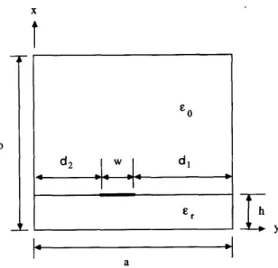
11. SUMMARY OF THE ANALYSIS TECHNIQUE Fig. 1 shows the microstrip structure used in this study. The strip conductor is assumed to be an infinitesimally thin perfect conductor. It is placed on top of a lossless isotropic dielectric substrate having a thickness h. The uniform microstrip line is then placed into a metallic waveguide housing of size a x b. The spacings between the strip and each of the two sidewalls, d , and d,, are arbitrary. The entire structure extends uniformly into infinity along both the
k
z directions.To determine the shielding effects on microstrip disper- sion, propagation of a Gaussian pulse along the shielded microstrip line is analyzed using the modified version of the FDTD method given in [7] and [SI. In this study, the
pulse width is chosen to cover the frequency range from dc to just below the cutoff frequency of the first higher order waveguide mode. For simplicity, the latter is ap- proximated by that of the structure shown in Fig. 1 but with the strip conductor removed 161.
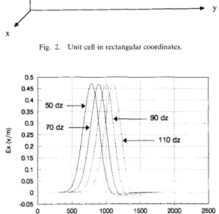
The FDTD technique proceeds by first segmenting the shielded microstrip structure into a three-dimensional mesh composed of a number of unit cells. Spatial and temporal discretizations of the electric and magnetic field components then follow. The positioning of the electric and magnetic field components about a unit cell in rect- angular coordinates is shown in Fig. 2. Temporal sam- pling instants for the electric field components and the magnetic field components are also interleaved, with a half time step separation between them. In this research, the spatial sampling interval is chosen to be one-eighth the substrate thickness, which has been found to yield converged and accurate results. To satisfy the Courant stability criterion [9] and to ease the implementation of the superabsorbing boundary condition [ 101, the time step is chosen such that the dc component of the pulse will propagate across one space cell in the z direction in five time steps.
A proper value of the permittivity is assigned to each electric field component of the lattice except for the field sampling points at the air-dielectric interface; here the average permittivity of the two media is used to satisfy the field continuity condition at the air-dielectric interface [SI. Appropriate tangential electric field components and
1689
E..
/---"
Fig. 2. Unit cell in rectangular coordinates.
0.5 1 I
-
E-.
Y W-
0.45 0.4 0.35 0.3 0.25 0.2 0.15 0.1 0.05 0 4 - 90dz ;+
11Odz 0 0 5 ~ " " " " " " ' " ' ' " ' " ' ' 0 500 1000 1500 2000 2500 Time StepFig. 3. Time waveforms of E, taken half a cell below the center of the strip conductor and at z = 50, 70, YO, and 110 cells away from the excitation plane. The strip is symmetrically placed between sidewalls and the size of the housing is 10h X 7h.
the normal magnetic field components are placed on the surfaces of the waveguide walls and the strip conductor; on the strip, only E , is allowed to be placed at the edge of
the strip. The boundary conditions are enforced by setting these field quantities to zero at all times. In addition, the superabsorbing boundary condition [ 103 is utilized to ter- minate the FDTD problem space in the direction of wave propagation.
The initial condition is such that a null field is present in the entire FDTD lattice except at the plane of excita- tion in which the Gaussian pulse has just arrived. It is further assumed that the excitation source is present only in, and distributed uniformly over, the portion of the substrate underneath the strip conductor [SI. Following this, a simple leapfrog time-stepping algorithm [ll] is employed to simulate wave propagation through the FDTD lattice.
Fig. 3 shows the space-time variations of E, observed at several locations (all half a cell below the center of the
strip) in the z direction for the centered strip case with a housing size of 10h x 7 h . It is seen that, owing to the dispersion in the microstrip structure, distortion in the pulse increases as it propagates farther down the line. The problem space is truncated at z = 120dz in this case. To check the performance of the superabsorbing bound- ary condition, the same structure is analyzed again with the problem space truncated at 200dz. Time waveforms of
E,
observed at z = 90dz in the two cases are com- pared. It is found that differences between the two wave- forms attain a maximum value of about 0.0002 V/m, o r about 0.05% of the peak value of E, observed atz
= 90dzshown in Fig. 3. Excellent performance of the superab- sorbing boundary condition is thus expected.
To determine E r e f f ( w ) for the shielded microstrip struc- ture considered, E , ( t ) at two different locations sepa- rated by a distance L in the z direction are Fourier transformed, with the resultant z-dependent spectra de- noted by E,(w, z = 0) and E,(w,
z
= L ) , respectively. Since only a propagating quasi-TEM mode is present in the frequency range considered, and both the strip con- ductor and the dielectric substrate are assumed to be lossless, the resultant spectra are related by the fre- quency-dependent phase constantp ( w )
as follows:E x ( w , z = L ) = E , ( w , ~ = O ) e - 1 ~ ( " ) ~ (1)
where
These equations are used to determine E r e f f ( w ) from the
FDTD simulated results.
111. RESULTS AND DISCUSSIONS The results to be presented in this section are all obtained for a strip having a unity strip-width-to-sub- strate-height ratio (i.e., w / h = 1) placed on top of a 0.635-mm-thick alumina substrate with E , = 9.7. Centered strip geometry is used when examining the effects of the two symmetrically placed sidewalls. The structural sym- metry consideration indicates that a magnetic wall is present at the plane of symmetry (i.e., y = a / 2 ) , which thus reduces the problem space by half. On the other hand, an off-centered strip position is used for investigat- ing the effects of a single sidewall. In this case, one of the sidewalls is placed far from the strip conductor such that it will not interact with the fringing field lines originating from the strip. The spacing between the second sidewall and the strip is then varied within a range where interac- tion between the two is expected. The additional top-cover effects are studied by adjusting the height of the housing simultaneously.
A. Centered-Strip Structures
Before the effects of a single sidewall and the com- bined effects of top wall plus one sidewall are investigated
Fig. 4. Plot of E, (0 < x d 6 , a / 2 d y < a ) for a centered-strip struc-
ture having a housing size of 10h x 7h when pulse reaches the maximum
at a half cell below the strip.
by analyzing the entire structure, an extensive numerical experiment is undertaken with the strip conductor cen- tered between the two sidewalls (i.e., d , = d , ) . Results obtained from this set of experiments characterize the effects of two symmetrically placed sidewalls and/or top cover, and from these one can identify the minimum sidewall and top wall spacings required so that their interactions with the fringing fields can be ignored.
Ranges of a
/
h from4
to 12 and of b/
h from 2 to 8 are used in this set of experiments. It is found that, for allb / h ratios considered, E r e f f ( w ) remains essentially un-
changed when a
/
h exceeds about 10 (i.e., d ,/
h = d ,/
h3
4.5).
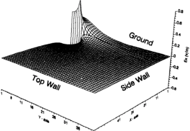
Fig.4
shows the spatial field distribution ofE J x , y ) taken for a housing size of 10h X 7h when E,
half a cell below the center of the strip conductor reaches its maximum value. It is found that fields are concen- trated mainly in the immediate surroundings of the strip conductor; no field line is found to terminate at the top wall. However, small amounts of E, do exist along the air-dielectric interface between the edge of the strip and the sidewall. Apparently, this latter phenomenon does not perturb to any significant degree the field distribution of E, half a cell below the center of the strip, and E r e f f ( w ) remains essentially unchanged when a
/
h exceeds about 10.The effects of the top cover alone can then be deter- mined, and these are summarized in Fig.
5
for a / h = 10and b / h from 2 to 7 . The figure shows clearly that the
effects of the top cover alone may be ignored in calculat-
ing 7 because, as shown in Fig.
4,
nofield line can reach the top wall. On the other hand, the effects of the top cover become quite significant when
b / h is less than
4.
This is more obvious at low frequen-cies as the wave-guiding capability of the strip is weaker and more fringing fields are present in the air region to interact with the top wall. Finally, by extrapolating the curve down to dc for the case of b / h = 2 (i.e., the strip is centered between the top and the bottom wall), a theoret- ical E r e f f value of 5.35 (i.e., ( E ,
+
11/21 is obtained.WU AND CHANG: CHARACTERIZATION OF SHIELDING EFFECTS b h = 7 b h = 6 b h = 5 b h = 4 b h = 7
-
bi=2 0 I O 20 30 Frequency (GHz)The effects of lowering the top cover for fixed U / h = 10 (i.e.,
d , / h = d , / h = 4 . 5 ) .
-
10 20
Frequency (GHz)
Fig. 6. The effects of closing in the two sidewalls with the norm red sidewall-to-strip spacing d , / h = d , / h = ( a / h - w / h ) / 2 . The top- cover height is fixed at h / h = 7.
Based on the above observations, the effects of two symmetrically placed sidewalls (i.e., d , / h = d , / h ) can then be examined from the E , . , , . ~ data shown in Fig. 6,
which are obtained by fixing b
/
h = 7 while varying a/
hfrom 4 to 12. The figure shows that data obtained for
a / h = 10 and 12 are almost identical. On the other hand,
reductions in can be detected when a / h is less than
10 (i.e., d , / h = d , / h G 4.51, which decreases rapidly for
a / h G 8 (i.e., d , / h = d , / h G 3.5).
These observations indicate that for the centered-strip structure considered the effects of waveguide housing may be ignored when a housing size of 10h x 7 h is used.
To verify the accuracy of the FDTD method, results obtained for a housing size of 10h x 7 h are compared
with the open-microstrip data calculated from the closed- form formulas of Kobayashi 1121 and Hammerstad and Jensen [13] in Fig. 7. As can be seen, our data are in good agreement with those calculated using Kobayashi’s for- mula over the entire frequency range considered for the shielded microstrip case. However, although Hammerstad
1691
7 1
8 -
1 -
-
Kobayashi [121Hanunerstad & Jensen [I31
-
This Research (a = 10h, b = 7h)I
6 ! . 8 . 3 . 9
0 10 20 30 40 50
Frequency (GHz)
Fig. 7. Comparison of e , , J w ) obtained from this research for a centered-strip structure having a housing size of 10h X7h with the open- microstrip data calculated using closed-form formulas given in [12] and [13].
and Jensen’s formula results in a comparable at lower frequencies, it yields much higher values of ereff at higher frequencies. Since the E r e f f ( W ) data used in the development of the dispersion formula in [12] are calcu- lated from a rigorous spectral-domain approach with carefully selected basis and weighting functions [14], they are considered to be more accurate. As such, this compar- ison confirms the accuracy achievable by the FDTD method.
B. Off-Centered Strip Structure
In view of the results observed in the numerical experi- ments performed for the centered-strip structures, the effects of a single sidewall, with and without any addi- tional effects of the top cover, may be characterized by using an off-centered strip geometry with d , / h = 4.5
(fixed), d , / h
<
4.5, and b / h G 7. Results thus obtained are compared with those determined for the centered-strip case with a/
h = 10 and b/
h = 7 , for which both the topcover and the two sidewalls may be ignored.
As our first example, results obtained with d ,
/
h vary- ing from 3.5 to 0.5 for b / h = 7 are shown in Fig. 8. It isnoted that, since the top wall and one of the two sidewalls are far enough away so that they do not interact with the strip conductor, e r e f f ( ~ > obtained for d , / h
<
4.5 can be regarded as the odd-mode E r e f f ( u ) for unshielded paral-lel-coupled microstrip lines spaced 2 d , / h apart. To bet-
ter illustrate the effects of a single approaching sidewall, data obtained for the centered-strip case with d , / h = 4.5
are also plotted in Fig. 8. It is found that the effects of a single sidewall are insignificant when d ,
/
h = 3.5 butbecome quite significant for smaller d , / h . Furthermore,
an examination of the data shown in Figs. 6 and 8 indicates that, for d, / h = 3.5 or 2.5, the amount of
decrease in E r e f f ( W ) almost doubled when two symmetri-
cally placed sidewalls are present compared with the corresponding single-sidewall cases. However, the reduc-
(2.5,3)
-
(1.5,3)-
(0.5.3) -*- 8 7- 6 --
-
d2h.I = 4.5 dUh=3.5-
dUh= 2.5 ----b-
d2/h= 1.5 dUh=0.5 5-1 I 0 10 20 30 Frequency (GHz)Fig. 8. The effects of a single approaching sidewall for the case of off-centered strip geometry with fixed b / h = 7 and d , / h = 4.5. tion factor is less than 2 when d , / h = 1.5. This suggests
that the effects of a single sidewall and those of two symmetrically placed sidewalls should be addressed sepa- rately.
As the top cover height is lowered to b / h = 6 and 5, results almost identical to those shown in Fig. 8 are obtained for each of the four d , / h values considered,
which indicates that the effects of the approaching side- wall prevail when b / h > 5 . However, by comparing the
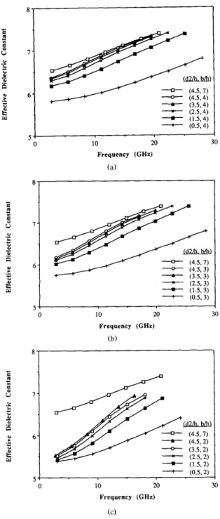
results obtained for b
/
h = 4 shown in Fig. 9(a) with thecorresponding data shown in Fig. 8, it is found that the approaching top wail results in a further reduction in The amount of reduction is found to be larger at lower frequencies and for larger values of d , / h as more
fields are present in the air-filled region of the structure to interact with the approaching top lid. Finally, parts (b) and (c) of Fig. 9 show that, for each of the four d , / h values considered, much smaller values of E,,ff are ob- served as the top cover height is further lowered to
b / h = 3 and 2.
C. Remarks on the Computational Aspects of the
FDTD Method
It is generally recognized that the FDTD method, while being able to solve a wide range of problems with a minimum mathematical preprocessing effort, is highly de- manding computationally. Take this study, for instance;
140 cells (with 6 = h
/8>
were used along the z axis for the data presented here. In all cases, data converging to within 1% were obtained when E J w ) taken for t>
1106were used in (1). For the case of a centered strip with a large housing size of 10h x 7 h , the total mesh dimensions
in the x, y , and z directions and the total time steps simulated were 40 X 56 X 140 X 2500. The CPU time for this particular problem was about 6 h on an IBM RS 6000/320 workstation (which is rated at 27 MIPS/7.5 MFLOPS). In another test, a CPU time of 20 min was measured when the housing size was reduced to 4h x 2 h ,
-
(3.5.4)-
(2.5;4)-
(0.5.4) (1.5.4) 0 10 20 30 Frequency (GHz) (a)-
( 4 . 5 7 )-
(4.5,3)-
(3.5,3) 7 - 6 - . U-/
-
/
/
P-
(0.5,2) 5 0 10 20 30 Frequency (GHz) (C)The combined effects of a single sidewall plus the top wall, with
d , / h = 4.5 fixed, for (a) b / h = 4, ( b ) b / h = 3, and (c) b / h = 2. Data obtained for the centered strip case with housing size of 10h x 7 h are also shown in each case for comparison.
for which the mesh dimensions were 16X16X140 in space and 2000 in time.
As evidenced by the field plot shown in Fig. 4, rapid variation in the field distribution is expected only near the strip conductor, use of a 3-D variable mesh scheme for improving its computational efficiency may be justified. In
WU AND CHANG: CHARACTERIZATION OF SHIELDING EFFECTS 1693
this regard, an extension of the 2-D local mesh refine- ment scheme described in [15] deserves further attention.
IV. CONCLUSIONS
The FDTD method has been employed to investigate the effects of shielding on the dispersive properties of a waveguide-shielded microstrip line on alumina substrate. Both centered and off-centered strip geometries have been examined to identify the effects of (1) the top cover alone, ( 2 ) two symmetrically placed sidewalls, (3) a single sidewall, and (4) the top wall plus one sidewall. For the centered-strip cases, it is found that the top cover may be ignored in calculating c r e t t ( w ) when b / h 7. On the other hand, the sidewall effects are insignificant when the spacing between the sidewall and the edge of the strip exceeds about 4.5 times the substrate thickness. For the off-centered strip cases, it is observed that the shielding effects are mainly due to the approaching sidewall when
d , / h
<
4.5 and b / h>
4. On the other hand, the com- bined effects of a single sidewall plus the top cover should be considered when d ,/
h<
4.5 and h/
h<
4. Finally, compared with the effects of a single approaching side- wall with d , / h = 3.5 or 2.5, reductions in E , ,Jw) almost double when two sidewalls with d , / h = d 2 / h are pre-sent.
REFERENCES
[I] T . C. Edwards. Foundations ,for Microstrip Circfut Design. New York: Wiley, 1981.
[2] S. March. “Microstrip packaging: Watch the last step,” Microwa/~c,s.
pp. 83-94, Dec. 1981.
[3] R. K. Hoffmann, Handbook qf Microw,ui.e Integruted Circuits.
Nonvood, MA: Artech House, 1987.
[4] E. H . Fooks and R. A. Zakarevicius, Microwur~e Eilgineering U.sing
Microsfrip Circuits.
[5] J. Moore and H . Ling, “Characterization of a 90“ microstrip bend with arbitrary miter via the time-domain finite difference method.”
IEEE Trans. Microwuc,e Tlieory Tech.. vol. 38, pp, 405-410. Apr. 1990.
[h] L. P. Dunleavy and P. B. Kdtehi. “Shielding effccts in microstrip discontinuities,” lEEE Truns. Microwuw Theoiy Tech., vol. 36. pp.
1767-1774, Dec. 1988.
[7] X. Zhang, J. Fang. K. K. Mei, and Y. Liu, “Calculations of the dispersive characteristics of microstrips by the time-domain finite difference method,” IEEE Trans. Microwac.e Theory Tech., vol. 36, pp. 263-267. Feb. 1988.
[8] X. Zhang and K. K. Mei. “Time-domain finite difference approach to the calculation of the frequency-dependent characteristics of microstrip discon ti nui ties,” IEEE Truns . M i c r o w c ,e Theory Tech .
.
vol. 36. pp. 1775-1787, Dec. 1988.
Englewood Cliffs, NJ: Prentice-Hall, 1990.
[ Y ] A. Taflove and M. E. Brodwin, “Numerical solution of steady-state electromagnetic scattering problems using the time-dependent Maxwell’s equations,” IEEE Trans. Microwace Theory Tech., vol. MTT-23. pp. 623-630, Aug. 1975.
[IO] J. Fang and K. K. Mei, “A super-absorbing boundary algorithm for solving electromagnetic problems by time-domain finite-difference method,” in IEEE AP-S Int. Symp. Dig., June 1988, pp, 472-475. [ l 11 K. S. Yee, “Numerical solution of initial boundary value problems
involving Maxwell’s equations in isotropic media,” IEEE Trans. Antennas Propagut., vol. AP-14, pp. 302-307, May 1966.
[ 121 M. Kobayashi, “ A dispersion formula satisfying recent require- ments in microstrip CAD,” IEEE Trans. Microwam Theory Tech.,
vol. 36, pp. 1246-1250, Aug. 1988.
[13] E. Hammerstad and 0. Jensen, “Accurate models for microstrip computer-aided design,” in IEEE MTT-S Int. Microwwe Symp.
[I41 M. Kobayashi and F. Ando, “Dispersion characteristics of open microstrip lines,” IEEE Trans. Micruwace Theory Tech., vol. MTT- 35, pp. 101-105, Feb. 1987.
1151 I. S. Kim and W. J . R. Hoefer, “ A local mesh refinement algorithm for the time domain-finite difference method using Maxwell’s curl equations,” IEEE Truns. Microwaw Theory Tech., vol. 38, pp. 812-815, June 1990.
Dig.. 1980, pp. 407-409.
Lin-Kun Wu (S’81-M’85) was born in Hsinchu, Taiwan, Republic of China, on November 1, 1958. H e graduated from the Taipei Institute of Technology in 1978 and received the M.S. and Ph.D. degrees in electrical engineering from the University of Kansas, Lawrence, in 1982 and 1985, respectively.
From November 1985 to December 1987, he was a Postdoctoral Research Associate at the Center for Research, Inc., of the University of Kansas working on microwave remote sensing and computationdl electromagnetics Since February 1988, he has been nn Associate Professor at the Institute of Communication Engineering, National Chiao Tung University, Hsinchu, Taiwan His current research interests involve the development of the finite-difference time-domain method nnd the method of moments for the characterization of mi- crostrip and waveguide discontinuities and for the analysis of electro- mdgnetic scattering problems H e is also interested in radar systems and rddar remote sensing.
Yeung-Chung Chang was horn in Sanchung, Taipei, Taiwan, Republic of China, on Novem- ber 18, 1966. H e received the B.S. degree in communication engineering in 1989 from Na- tional Chiao Tung University, Hsinchu, Taiwan, where he is currently working toward the M.S. degree. His B.S. and M.S. theses deal with the analysis of satellite antenna and the characteri- zation of shielding effects on microstrip disper- sion. His research interests include antennas, radar, and fiber optics.
![Fig. 7. Comparison of e , , J w ) obtained from this research for a centered-strip structure having a housing size of 10h X7h with the open- microstrip data calculated using closed-form formulas given in [12] and [13]](https://thumb-ap.123doks.com/thumbv2/9libinfo/7519798.118610/4.928.483.790.111.340/comparison-obtained-research-centered-structure-microstrip-calculated-formulas.webp)